Note: Descriptions are shown in the official language in which they were submitted.
3~
ME:THOD AND APPARAT S FOR RE:COGN171NG ~EFECTS
IN A TRIGGERING SYSTEM OF A
CONTROLLEO SERIES COMPEI~ISATOR
BACKGROUND OF THE INVENTION
The present invention relates to a method and a ~levice for recognizing
~lefects in a triggering system of a controlle~ series compensator.
In series compensation systems, capacitors are usually employed in the
wiring run to reduce the current-dependent voltage llrop across the line and thetransmission angle, in steps. These capacitors are capacitor banks, which are
switched on and off in series, as a whole or in several capacitor sections
(segments). The capacitor is switched )n and off by opening or closing a
l(~ par.lllel circuit-hreaker. In case of a short-circllit on the network, a parallèl
arrester, a tri~erahlc spark ~ap, an(l/or al parallel circuit-bre;lker ~uaranteerotection for the capacitor
Furthermore, a series compensation system is known, in which by means
15 of an insluctor connected in parallel with the capacitor, the total impedance of
this series capacitor, similarly to the case of a 1 CR (thyristor controlled reactor)
in the static compensator, is steplessly controlle(l with a current-converter valve
to high-voltage potential through appropriate triggering A series compensator
controllell in this manner is known as an ASC (Advance~l Series Compensation~,
'l) A series compensator controlle~ in this manner allows lhe dynamic response of
the series compensation u) l~e improved, and the total impedance is ahle to l~e
controlled automatically within a certain range, whereby the impe-Jance can be
,, ~ ' ',- .
- ~ ' ' . ' ~ ~ ''
. .
,
.
2~
changed from capacitive to inductive impedance.
These types of series c;3pacitors are introduce~ in tl1e essay Automa~ically
Controlled Par~llel~ Series C'ompensa~ion [Cere~elte Pcmlllel- uncl
Rei~lenkompensati~n], published in the German perio~icaJ, "Elektrie", Volume
~5, 1(~91, March, pp. 88 ~hrough 9(). In a~ldition, the International Patent WO
~7/()4538 (lescribes a series capacitor, which is controlled in such a manner and
is integrated in a transmission line.
I() The irnpedance of the series compensator is adjusted by influencing the
firin~ angle of the current-converter valve, which is electrically connecte(l inparallel via a coil to the series capacitor of the series compensator. The current-
converter valve consists of two antiparallel connected valves, wllic}l are each
comprised of several series-connected valves. The impedance to be adjusted is
1~ predetermined by primary coordinating (conduction current control, load voltage
control, oscillation damping). In an arrangement of the series compensator in
a three-phase voltage system, the impedance to he adjusted is of the same
magnitude in the three phases. The firing angle ~, which applies to the
alternating componenl of the capacitor voltage, has a non-linear relation to the20 impedance.
When there are defects in the triggering system of the valves, it can be
that the impedance of the controlled series compensator does not equal the
setpoint impellance required by a closed-loop control or by an open-loop
25 control. This state of the controlled series compensator results in disadvantages
t`or the network (usymmetry, une~lual loa~ling of the lines"~ifferent degree of
compensation~. It can happen that the advan~ages of the controlled series
compensator are lost, or that these advantages turn into disadvantages.
~(~ Therefore, this fault condition in the controlled series compensator must
he ahle to be Lletected hy the series compensator itself, since this ~ault condition
Call ollly he letec~ed wi~h ~lle exis~ing devicer in ~he ne~work af~er a ~lelay or
:`
. . . .
- , . ~ .
.
X~9~
it c~nnot be (letected ~t all. Thus, the controlled series compensator requires
a self-monitoring system.
Defects in the triggering system often result ;n a change(l firing
S performance for the current-converter valve, ~, the current-converter valve isl rought into circuit after a delay or not at all. C)f the possible (lefects, one
special case would be the failure of the valve electronics at a single valve
location. The valve can only be brollght into circuit by operating the overvoltage
damping diode, also known as a break-over diode (BS:)D), which serves as
1() overvoltage protection. The operating response voltage of an overvoltage
d,lmping diode is only slightly less than the maxirnum positive blocking voltageof the corresponding valve. In dependence upon the level of the capacitor
voltage of the series capacitor of the controlled series compensator and upon the
firing angle, the operating voltage of the overvoltage damping diode is reached
15 and she valve is hrought into circuit with delay. If the operating voltage of the
overvoltage damping diode is not reached at other system working points, the
result is a firing failure, whicll means that the controlled series compensator only
still has a restricted control range at its disposal.
~() Apart from the mentioned case, all defects in the triggering system result
in a failure of the valve firing.
Faults in the closed-loop control system and in the triggering system must
l-e ~etected by devices of the controlled seriçs compensator andt in this respect,
?5 lhiS series compensator musl he ~7roll~ht into a s~ate in which ~lisa~lvant"~es for
the network operation are avoi(led.
SUMMARY OF THE INVENTION
l'he present invention relates to a method and an apparatus which allow
3() defects in a tri~gerill~ system of a controllesl series compensator to 17e
reco~nize~l and the controllçd series compensator to be brought, in this respect,
into sllch n state that dis.ldv.lnta~es will 17e aYoi~led for the netwnrk operation.
.
.'
2~9~
Defects in the triggering system of a controlled series compensator occur
rall~lomly, ~, in(lepen~ently of the oper~ting mode - steady-state operation~
TCR oper~lion (thyristor controlle(l reactor), TSR operation (thyristor switche~3
reactor). To (letect SllCh (lefects in Ihe triggering system of the controlle~J series
:) compensator, comparing the impe~lance of the series compensator would providea soiution. When the controlled series compensator is functioning properly, it
can be assumed that in the steady-state operation, the currently active
impedance conforms with a specified setpoint impedance. The currently active
imped"nce can be calculated from available measure(l values (conduction
1() current, capacitor voltage). The differential value for irnpedance that is
formulated can either be ol)served for an appropriate time span and/or be
compared to a limiting value. If the differential impedance value is present
l-eyon(l this time span and/or exceeds the limiting value, then an intervention
must be made into the triggering system, since a defect exists.
The type of intervention is dependent upon the voltage level of the
measured conduction current. If the conduction current is smaller than a
Iimiting value, the firing is blocked in all branches, since the voltage across the
series capacitor woukl never attain the operating voltage of the overvoltage
2() protection because of such a small conduction current. If the conduction current
~' is gre;lter than a limiting value, then the firin8 angle is limite~l in all branches
to ~ value that is (lepen(lent upon the voltage level of the measured con(luction
current, so that the v~lve can he brought into the circuit by means of protective
firing, If the valve is brought into Ille circuit by means of protective firing, this
is si~l);lile(l to the valve~ se electronics of the triggering system. In this case,
~` u stal)le TCR operati(ln having a restricted control range is possible. If in spite
of sutficient con(luction current, the valve is not brought into the circuit,
neither the protective firing is signalled nor is the impedance differential
re(luce(l, then the firin~ is blocked in all branches.
,. By evaluating network variables an(l comparing them to reference
vari,lhles, tlle method an~l apparatus ~ccor~ling lo the present invention
::
-
.
., .
;. . . . .
~9f~
intervenes to control the manipulated variable (impe-lance or firing angle) of the
controlled series compensator. Besides detecting valve malfunctions ~y
evaluating network variables and manipulated variahles, this melhod ~Iso ~letects
instances of asymmetrical triggering of a controlle(J series compensation system5 in a three-phase network. This method increases the availability of the system,
as well as the quality of the compensation through symmetrical operation.
Other possible ways for monitoring the valve firing, for example
comparing the firing pulse to the subsequent current flow in the valve or
1() evaluating the check-back signal from a protective firing that has taken place,
do not furnish any information or only provide uncertain information depending
upon the system working point of the controlled series compensator.
According to another method, a firing-angle signal is generated, as soon
15 as the measured capacitor voltage exhihits a direct voltage component, and the
value of the measured valve current of the controlled series compensator is lessthan or equal to a lower limiting value, whereby the value of the firing signal is
dependent upon the level of the conduction current to such an extent that a
protective firing can take piace. The failure of a valve leads in the series
2() c;lpacitor of the controlle(l series cornpensator to a direc~ voltage component,
which can be recognized in the measured capacitor voltage. Moreover, in case
of a failure of the current-converter valve, the valve current falls l~elow a low
limiting value or equals zero. Consequently, this methocl is used to detect valve
failures, which are not able to be recognizecl by means of valve electronics. In25 this case as well, network variables are evaiuate(l and comparecl to reference
v.ariables, ~ faults in the closed-loop control and in the triggering system are~letecte~l by devices of the controlle(l series compensator and, as a result, this
series compensator is l-rought into such a state, that disa(lvantages for the
networli operation are avoided.
3()
One particlllarly aLlvantageolls emhodiment of the apparatus for
implementing îhe method for recognizing defects in a triggerin~ system of a
S
,
controlled series compensator according to the present invention provides for
the device to he a microcomputer. Since it is preferable for the forward
colltrolling elemellts all(l tlle colltrollill~ system of a controlle(l series
compensator to he a compllter system, the appar.ltus includes a pro~ram which
recognizes defects in a triggering system.
To further clarify the method an~l the apparatus according to the present
invention in which defects are recognize-l in a triggering system of a controlled
series compensator, reference is made to the (Irawings, in which exemplified
1() embodiments of an apparatus according to the present invention are
schematically illustrated.
BRIE~ DESCRIPl'ION OF THE DRAWINGS
FIG I illustrates a controlled series compensator and an apparatus for
15 recognizing defects in its triggering system according to an embodiment of the
present invention.
~ IG 2 more closely depicts as a block diagram the structure of the
apparatus for recognizing defects according to the embodiment of the present
2() invention illustrated in FIC 1.
FlG 3 illustrates in greater detail a block diagram of an advantageous
specific embodiment of the apparatus according to FIG 1.
~5 DETAILED DESCRIPTION
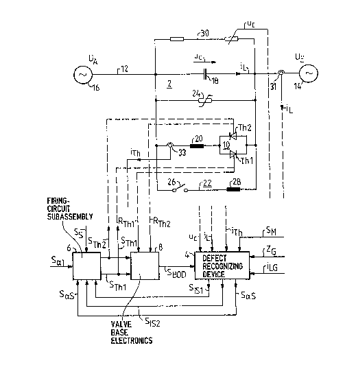
FIG I depicts an equivalent circuit diagram of a controlled series
compensator 2 having a device 4 for recognizing defects in a triggering system
of the controlled series compensator 2. Only one firing-circuit subassembly ~5
nnd one valve-base electronics circuit 8 from this triggering system are illustrated
~() hl I~IG 1. The firing-circuit suhassembly ~), which assures a ~ime-synchrtlnous
Iri~L~etin~ ~1 51 cllrre~ collverter valve 11) of the colltrolled series compensator
'~ is connecte(l on the outpllt si(Je to the valve-h.lse electronics ~, which is
. ,
.
., . ., ~ .
.
' :. . : ' . '` ' `'` ~ '
"r3~
elect~ocon(luctively connecte~ on ~he output side to the ~levice 4. This firing-circuit su~-assemhly ~ transmits firing signals Slhl an(l S~ for the v~lves Thl and
Th~ of Ihe current-conv~r~er vnlve 1(), whicll ,Ire pro~ ce~l frnm a synchronizing
sign.ll S~ all(J a firinL~Aan~le si~nal Sl, which c()rrespon(ls to ~ (lesire~l firin~ angle
S cy. The controlle(l serie.s compensator 2, ~vhich is also known as ASC (Adv~nced
Series Compensation), is brought into the circuit ~s a series resistor in a
transmission line 12. In most cases, this occurs along line 1~, but also takes
place at the outpu~ or input of switching substations. Voltage sources 14 an~ 16are in~icated at the beginning an-l the en(l of the transmission line 12,
I() respectively. The voltages UE and UA of voltage sources 14 and 16, respectively,
differ in amplitude by a line-voltage drop ~U and are phase-displaced in a
voltage angle of rotation (or phase angle). The voltage IJA across the beginningof the line is also described as a transmitting voltage UA, and the voltage Ue
across the end of the line is also described as a load voltage UE.
The structure of a controlled series cornpensation system 2 can be
sub(iivided into three regions. The core of such a system 2 consists of a seriescapacitor 18, which is integrated serially in the transmission line 12. In this
manner, the inductive series impedance of the line 12, which is responsible for
~() the in(luctive reactive-power component, is compensated for. In the case of a
controlled series compensation system 2, a branch consistin~ of a reactor 20 andn converter valve l() is ad-~itionally connected in parallel A parallel connection
of two thyristor valves Thl and Th2, which are arranged antiparallel to one
allotller, is ~iepicte~l as the converter valve 1(). By means of these two thyristor
~5 v;llves Th I and Th2, the reactor 2() can be bro1l~ht into circuit al preset times
for the positive an~ negative half-wave of the voltage UC Of capacitor 1~. In
place of the thyristor valves Thl and Th2, oth¢r semiconductor valves can also
l-e use~, such as GTO-thyristors (gate-turn-off thyristors). The structure of a
thyristor valve for reactive-current compensation is published in the essay Power
3(~ Converters for Stutic Re~tive-Current Compensation [Str~mricllt~r fi'lr sta~isclie
B~ stl-Q~7tkO~7tpel75atiOn] in the German pqrio~lical "Siemens-EIler~ietechnik",
volume 3 (19~1). issue 11 an~ , pp. 353 - 357.
. ~ . ~ . , ,
.. . . .
. . . . .
-, .
- .
.
By me.ltls of tlle hral1cll it is possihle for the effective impe~lance o~ tlle
controlle(l series compellsa~l)r 2 ~o 17e continually chlnged capacitively all(lin(luctively thrr)u~ll a ph.lse-.lngle control In this manner hesicles incre.lsillg
Irallsmissioll power one i~s also al)le to Ihl1it a short-circlJit current oll line 12
'i in case of a fault The a~lvantages enulllerated in the textbook Senes Capa(itor~
in Electric N~twork~ [ReilZe~lk~lt~/e~1.s~t(~ren i~l elektrisclle)1 Netzen] hy Dr-Eng
I eollllar(l I\/liiller 19(~7 I)a~e ~ assl)ci.lte~l with the al~plic.ltioll Or scrie.s
cap.lcitors also apply to a controlle(l series compensator 2
I() T(l protect tlle series cap.lcitor 1~ the reactor 2() all~3 the convel ter ~alve
1() ~rolll overloa~ls cause~l by higll con~luctioll currents i, a by-pass patll 22 all~l
a noll-linear resistor 24 (also known as an arrester) are installe~ in parallel witl
capacitor 1(~ and the series comhination of reactor 2() and converter valve 1()
~ met.ll-oYi(ie varistor (MOV) may Ite provi(led for example as the non-linear
l 5 r esistor 2~ Ihis metal-oYille varistor (24) wllich is conllecled electrically
p ar.lllel to the series ca,~)acilol 1(~ is (linlellsiollally ~Icsi~lle~l lo allow allcslel 2~
to lal;e over the current con~luctioll very (luickly al a pre~letermine(l vollage
alllplitude Conse(luently it protects the series capacitor 1~ from longer lasting
overload conditions The energy absorption capacity of a non-linear resistor 24
2() is naturally limited due to economic consi-lerations Therefore a series
compensation system 2 must also be capal-le of protecting the series capacitor
1~ with its arrester 24 from overloa~ls Tllis task is assumed hy the par.lllel l-y-
pass path 22 This by-pass path 22 consists of a by-pass switch 26 and a ~lalllphl~
circuit 2X In place of the by-pass switch 26 a triggerable spark gap or a
25 comhination of the two can be provi~led The by-pass switch 26 îs close(l as SOOn
as the loa~lin~ ~ the energy ahsorption capacity of the arrester 24 is
e:l~h.luste(l.
A potential ~livider 3() at whose output the capacitor voltage UC is applied
3() is similarlv provi(le~l electricallv parallel to the series capacitor 18
Tl-e actual value of tlle con~hlctioll current il is measured ill tl1e
. .
` '.
.. ..
.. -: . . : : :. . ..
-
: . , : .
.. . . . . . .
,
2~
transmission line 12 by means of a device 31, while on the other hand the actualvalue of the current iTh flowing through the coil 20 and the current-converter
v,~lve 1() is measured by means of a device 33 These system variables i~ and u~
al~ are carrie-l over a fiher-optic system in a n-anner that is potential-free
from the system ~, which is at high voltage potential, to the device ~ to
recognize defects in a triggering system of this system 2, which is ilt earth
potential This potentkll-free transmission of the system variables il, u( anLI ilh
is (lepicteLI hy a broken line
1() Also supplied to the defect recognizing device 4 for recognizin~ defects
are a mode signal S~, an impedance limiting value ZG, and a conduction-current
limiting value iLG The outputs of the device 4 are connected to the firing-circuit
sul~assemhly 6
FIG 2 depicts a block diagram of the defect recognizing device 4
according to FIG 1~ Defect recognizing device ~ consists on the input si~le of
a signal-conditioning device 3~ and, nn the output side, of a signal processing
device 34, which is connected to outputs of the signal-conditionin~ device 3~
In one advantageous specific embodiment of the defect recognizing clevice 4, a
2t) microcomputer is provide~J as the device 4
On the input side, the signal-conditioning device 32 has a processor
circuit 36 for calcIllating the effective, current impedance 7~j frnm the measured
capacitor voltage u(~ and the measured conduction current il A changeover
?5 switch 3X is also provi(led on the input sicle of signal-conditioning device 3~"1t
wllose hlpIlts the setpoint impedances Zxl and Z~ are applied, and at whose
control input the mode signal S~ is applied The outputs of the pr~)cessor circuit
3() anLI of the chan~eover switch 38 are linked via a comparator 4(~ to an
ohservation stage ~ and/or to a first comparator 44 The ou~put of the
3() i-rocessor circuit 3() is therel~y electrocondllclively connected to the negative
hlput ot the compurutl)r ~), an~l the ou~pllt of the chart~eover switch 38 is
connected to the positive input of the comparator 4(), An impedance limitinL~
., .
. . . . .
: . - , -
' ,,: .:, .. . ,' : . ,
,- - . . ~ , . .: ,. ~
,~
- ' . ,`
value ZG is applied to a second input of the first comparator aA On the output
side, comparà~or 44 is connecte(l to a first input of an OR-gate 46. The second
input ()f OR-gate 4() is linked tn the Outpllt of the ohservation stage 42, which
can l~e a proportional-action controller of the first order (PT~-controller), for
5 example
Moreover, on the input side, the signal-conditioning device 32 inclu~les
a second comparator 4~3 having a first input at which the measured con(luction
CUrrent jL ;S applied and a second input at which a conduction-current limiting
1() value i~ O is applied. The output of the OR-gate 46 and the output of the second
comparator 48 constitute the outputs of the signal-conditioning device 32.
On the input side, the signal-conditioning device 34 has a first AND gate
SU ancl a second AND gate 52, and a NOR gate 54. The first input of the first
lS AND gate 50 is electroconductively connected to the first input of the secondAND gate 52~ The second input of the first AND gate 50 is linked by means of
an inverter 56 to the second input of the second AND gate 52. Moreover, the
first input of the first AND gate 50 is connected via a further inverter 58 to afirst input of the NOR gate 54. The second input of this NOR gate 54 is
~() electroconductivety connected to the output of the valve-base electronics 8
according to FIG 1. The output of the first ANI) gate 50 is connected to the setinput S of an RS ~lip-flop fi(), whose output Q is linked to a first input of a
function generator 62. The measured con(Juctinn current il is applied at the
second input of the function ~enerator 62. A manual signal S~ , is applied to
~5 the reset input R of RS flip-flop h(). Tlle output Q of the RS flip-flop fi() is
connected via an observation stage 64 to a third AND gate 66. The second
input of the third AND gate h6 is connected to the output of the NOR gate 54.
As an observation stage fi4, a proportional-action controller of the first order(PT~ controller) can likewise be provi~ted whose time deJay is able to be
~) udjuste(l to a specifi.ll)le ohservalioll time. Tlle l)UtplltS of the characteristic
generator 62 and of the second an-l thir~l AND gates 52 und 66 constitute the
olltputs of the siL~nal-procexsill~ device 3~.
1()
.. .
` ` ~ '. `
..,
. . .
' ' : ~ " , . , '
2~
A signal processor can be used in each case as a signal-conditioning
device 32 and as a signal-processing ~levice 34, or a microcomputer can be
provi(le(l for b oth of them together. The sign.ll-processing device 34 can alsol~e ma~le ~Ip of other logic mo~ les.
On the basis of this block diagram of the defect recognizing device ~ for
recogllizing defects in a tri~gering system of a controllel3 series compensator 4,
the methn~l of operation of this (levice 4 will now be clarified in greater ~letail
in the following.
I()
As already mentioned at the outset, a proper functioning of the
controlled series compensator 2 can be assumed when its impe~arlce Zj
me.lsured in stea(ly-state operation conforms with a specified setpoint impedance
Z~l or Zs~. The currently effective impedance Z; is calculate(l from the
lS measured capacitor voltage u~. and the measured conduction current i~ of the
controlled series compensator 2 by means of the processor 36. In dependence
upon the mode signal SM, the changeover switch 38 relays the input setpoint
impedance Zsl or ZS2 to its output.
2() In a-ldition to the idle state as an operating mode of the controlle(l series
compensator 2, there are also the running operating modes: TCR operation
(thyristor contrnlled reactor) an~l TSR operation (thyristor switched reactor).
The current-converter valve 1() is periodically fire~l in TCR operation, wherebythe firing angle c~ is variahle. In TSR oper~tion, the current-converter valve 1()
~5 is continuously fired. In TSR operation, the setpoint impe(lance Zs~ is fixed and
corresponùs to the impedance of the parallel connection of the series capacitor
18 and of the coil 21) of the controlled series compensator 2, which is
si~niYicantly less than the impe-lsnce of the series capacitor 18. In TCR
oper.ation, impe~ance (iifferentials ~2:=Z~I-Z; occur in the non-steady-state
~) con~lition, even given a fault~free triggerin~ system. This is why the impedallce
~lifferential ~Z, which is determined by mean~ of the comparator ~(), must be
ol)serve~ for an appropriate time span, hefore a more far-reaclling intervention
,.
. . : , .
~ '. . .. . . . .
.- . .. .. -
:
.
,
can be derived from it. A PT~- controller can be provided as an observation
stage 42, whose ~ime delay is ~(ljusteLI to the appropriate time span If an
impe~lance LlifferelItial ~Z is present longer than the appropriate time span, then
a signal ~Z~, which corresponds to the impeLlance ~lifferential ~Z, appears at the
output ()f the observation stage 42. At the same time, the impe~ance
differential AZ can be compared by means of the comparator 44 to an
adjustable impedance limiting value Z,;. An output signal SKZ is applied to Ihe
output of the comparator 44.
I() If the imped~nce differential AZ has excee~led the impedance limiting
value ZG. or if this impedance differential ~Z is present for the appropriate time
span, so that this is nO longer acceptable for the network, the OLltpUt signal SOD
at the output of the OR gate 46 changes from a low level to a high level. This
means that an intervention must now be made. The type of intervention is
15 dependent upon the level of the conduction current ;L. Comparator ~8
determines whether the conduction current il is greater or less tharl an
adjustable conduction-current limiting value il ci~ A comparator signal SKI which
exhihits a high level is applied to the output of the comparator 48 when iL > il G.
Cnmparator signal SK~ exhibits a low level when i~ < i1(;. Signals SOD and S~c~
?() from the signal-conditioning (levice 3~ are fell to the signal-processing device 34
as input signals. Additionally, signal-processing (levice 34 is supplied with input
signals inclu~ling the measure(l con~iuction current il from cievice 31 alld
prl)tective-firing si~nal S13~ from the valve-hase electronics 8.
?5 TCR Operation:
If the level of the conduction current jL jS less than the limiting value i~ G
when a defect is detected in the triggering system of the controlled series
compensator 2~ then the level of comparator signal SK~ is low, the output signalS~,. from the first AND ~ate 5() is low an(l the level of the 011tpUt si~nal Sls"
lsl) c;lllell tlle first tirin~-plllse l-lockill~ siL~ , from 1he secon~l AND ~ate ~7
is high, thrnu~h which means the firin~ is hlocl~e-l in all hranches.
.
~ .
2~
If the level of the conduction current jL jS greater than the limiting value
il ~; when a Llefect occurs in the îriggering system, then the comparator signal SKI
is hi~l1 an~ output signal S/~N from the first AND gate 5() goes to a higl1 level.
This causes the output si~nal SAK from the RS flip-flop 6() likewise to jump to
a hi~h level By this means, a firing-angle signal Ss is determined in the
function L~enerator (.2 h1 ~lepen~ence upon the measure(l conduction current i,
in such a way that, as a result of the large con~luction current i~, the valve
voltage of the currel1t-converter valve l() runs up to the operatinL~ response
volt~e of the protective-firin~ (Jevice If the current-converter valve l() is fire~l
l() by means of protective firing, then this is signalled by the check-back signals
R~ and R~b2 to the valve-hase electronics X, which then feeLis a protective-
firing signal SBOD to the device 4. In this fault case ~, fault in one thyristorlocation), the current-converter valve l() is periodically fired via the overvoltage
~lio(le (BOD), so that a st~ble TCR operation having a limited control range is
15 possihle. In this fault case, the firing angle o~ is smaller than 180, and the
impe~lance Zj of the controlled series compensator 2 is greater than the
impe(lance Z~ of the series capacitor 18, whereby for the impedance Zj of the
controllecl series compensator 2: Zc < Zj < Z~. The impedance Z~ is always
distinctly greater than the impedànce Zc of the series capacitor 1~. However,
~() it is not a fixed value, but rather is ~lependent both upon the firing angle o~ and
~he con~uction current ;L as well as upon the operating mode tha~ is aLljusted
when the fault occurs (TCR operation with o~ < 1800 or rather i(lle state o~ =
l~()o) The impe(Jance Zj hetween the capacitor impe(lance Zc and the
impe~ ce Zl is n0t a~ stable, so that the result is an unstea~ly ~Iyrlamic
~5 ch,lr.lcteristic. Since perio~lic protective firin~ is ~letecte~l an~l signalle-l in the
valve-b,lse electronics ~, this ~ult case is cle~rly i(lentifieLI.
If in spite of ample conduction current jL. the current-converter valve lO
is not brought into circuit,~ there is neither a protective-firing signal SBOD nor
~1) a rc~lucliol1 in th- in~l)eltallce ~lifferelltial ~,Z (oulpllt si~nal SOl~ woulLI h;lve ~o
cll~n~e from hi~sh level to low level) A~ u re~;ult, the )utput si~n~l S~O~ from
îlle N()R ~ate ~4 ch.lll~es from low level to higll level, al1(1 the outpu~ sigl1.ll Sl~,
13
.
. . .
.. ~ : . . , . :
, -, . ~
' :' ,.,
~ ~5~
also called the second firing-pulse blocking signal, from the third AND gate 66
changes from low level to high level, since the output signal S~K from the RS
flip-flop h() was at a higll level for an approl)ri.lte ~ime sp~n. The firing ishlockeLI in ~11 hr;lnches hy means of this second firing-pulse blocking sign;ll S~s2.
.~
TSR Operation:
In the TSR operation, the setpoint impedance ZS7 of the controlled series
capacitor 2 is constant an(l correspon~ls to the impedance Z~ of ~he coil 20 of
tlle series capacitor 2. The amoullt of this coil impedance Zl is always
1() consklerably smaller than that of the capacitor impedance Z~. If the imped~nce
differential ~Z has been detected with certainty, ~, the OUIpUt signal SOD from
the OR gate 46 has changed from low level to high level, then the firing can be
hlocked in all branches, while taking into consideration the impedance symmetry
nf the system 2 given conduction currents of iL ~ iL,; (first firing-pulse blocking
15 signal S1~7 changes frorn low level to high level). If the conduction current is jL
~ jl (;~ then A firing-angle signal Ss is generated by means of the output signals
S,~N and SAK in a way that allows the valve voltage of the current-converter valve
1() to run up to the operating voltage of the overvoltage diode. If the current-converter valve 1(1 is hrought into circuit at this point by way of the protective
2() firing, then this is detecte(l hy the valve-hase electronics 8 and communicated
to the defect recognizing device 4 hy means of the protective-firing signal SI~OI)~
which changes from low level to high level. If in spite of ample conduction
current jL~ a perio~lic protective firing does not occur, then the prntective-firin~
S;~naI SIIOD remain~ at a low level, throu~h whicll meslns the second firing-pulse
~5 I-locl;ing signal Sls~ changes from low level to high levei by means of the outpu~
Sign;llS S~OR and S ~KI~ SO that the firin~ is hlocked in all branches of ttle system
Another hlock diagram of the slefect recognizirlg device 4 is depicted in
~(1 FlC ?~ in greater detaih C~mpared t-~ the l-lock diagram of the device 4
accordin~ to FIG ~ the ~efect reco~nizin~ (levice 4 in FIG 3 ~iffers, on the onehand, in that the signal-conditioning device 3~ includes ~ device 68 for
.
"
.
~9~
determining a direct-voltage component of the capacitor voltage uc of the system. Defect recognizing device 4 of FIG 3 aclditionally differs from device ~ of
FIG 2 in th~t the comparator 4~ now comp.ares the valve current i~ to a
limiting value ilh(j, which is very small nr e(luals zero. The signal-processing5 ~levice 34 illustrated in FIG 3 also includes an AND gate 70 having three inputs
an~l an output. The output of AND gate 70 is supplied to an RS flip-flop 60, theQ OUtpUt SAK of which is supplied as an input to downstream characteristic
generator 62.
I() If the output signal SOD from the OR gate 46, ~he comparator signal SK~,
and the output signal Sl~c from the device 68 are at a high level, then a fault is
present in the triggering system, because either the impedance differential AZ
w.as present long enough or it is greater than a limiting value Za, ur because no
cnrrent iTh flows through the current-converter valve 10, and the capacitor
IS voltage uc exhibits a direct-voltage component, as a result of a defect in the
current-converter valve 1() (failure of a firin~ tlevice). As a result, the output
signal SAN from the AND gate 7n changes from a low levçl to a high level,
throu~h which means a firing-angle signal Ss is generated by means of the
output signal S,~K from the FtS flip~flop 60 and by means of the con~uction
2() current iL. This firing-arlgle signal S~s results in a protective firing.
By rneans of the methotl and apparatus according to the present
hlvention, (lefects in the trig~ering system of the controlle~l series c~pacitor are
recognized. As explained above, these defects result in:
~5
- asymmetry;
unsteadiness of the t~ynamic characteristic; hunting in the closed-loop
control;
- overloa(ling of valve components
Often, unfavt)r~le instances of con~lucte~l interference are m;~nifeste~l on
he network. Therefore, the necessity arises to intervene in accordance with the
-
;~9~
method and apparatus of the present invention. The possibilities are:
- Blocking the firing in the (lefective hr.lncll; an impe~lance asymmetry is
accepted thereby;
5 - Firing-pulse blocking in all branches;
- Activating a limiting characteristic in all branches; a TCR operation
having a limite~ control range can then be carrie~l out.
16