Note: Descriptions are shown in the official language in which they were submitted.
S-~092/19014 PCT/US92/02g72
` 209~.19
Description
Semiconductor Light Source Temperature Control
Technical Field
This invention relates to temperature control
devices, and more particularly to such devices for
controlling the temperature of a light source
fabricated on a semiconductor substrate.
BacXground Art
A fiber optic gyroscope (FOG) includes a source of
light energy, e.g., a laser diode, which provides
coherant light split into two beams that are launched
into each end of a coil. When no rotational
disturbances are present, the beams propagate Pqually
in opposite directions around the coil and recombine to
form an interference fringe pattern at a detector.
When the coil is subject to a rotation about an
axis normal thereto, a nonreciprocal disturbance occurs
known as the Sagnac effect, whereby the opposing light
beams take di~ferent times to traverse the coil. This
causes a phase difference between the beams and a shift
of the fringe pattern. The magnitude and direction of
the fringe shift is proportional, respectively, to the
rate and sense of the rotation applied to the coil.
A phase difference between the two beams can be
compensated for (i.e., nulled) by imposing a further
nonreciprocal phase shift on the beams in an equal and
- opposite manner by using a phase modulator, e.g., a
lithium niobate integrated optic phase modulatnr. In a
serrodyne closed-loop FOG, a phase modulator is driven
by a linear ramp or a step ramp signal. The modulator
.. .. -- . : : . ... .
W~2/19014 PCT/US92/029~ i
~, ~ 9 ~
induces a phase shift in the light passing through
which is equal and opposite to the Sagnac phase shiftO
When the magnitude of the ramp is held constant to an
amplitude corresponding to one wavelength, and the
duration of flyback time is approximately zero, gyro
rate in~ormation is given by:
n = (SF) * ~f)
where n is the angular rate of gyro rotation, f ls the
frequency of the linear ramp, and SF is a scale ~actor.
The ramp frequency can be directly measured t and
the scale factor is a ~unction of the source
wavelength. In turn, the source wavelength is a
function of the source temperature, e.g., 0.03%/oc for
a laser diode. Thus, it is important to know the
source temperature so that either a scale factor
correction can be made for changes in temperature, or
the source temperature may be controlled to maintain a
constant wavelength and scale factor.
Some known packaged semiconductor light sources
comprise a temperature control loop consisting of a
thermistor mounted to a substrate or package surface
for measuring source temperature, and a means to cool
the source package, such as a thermo-electric cooler.
The cooler attempts to maintain the source at a
constant temperature, thereby removing
temperature-induced wavelength variations.
However, the thermistor does not directly measure
the source's temperature, which results in two types of
error. A steady-state error occurs due to the thermal
resistance between the thermistor and the source. This
error may vary further with the source's efficiency,
which can change due to aging. A second type of error
is delayed response caused by thermal transport lag and
, : ' , ' - ' ' .
.: ~ ' : :
. . . - - , .
~` ` 2 0 9 ~ ~ 1 9 PCT/US~2~0~972
the thermistor time constant. This error is most
prevalent during system power up and source power
transients.
Further, the cooler is part of the thermistor
package and not the substrate itsel~. As such, the
cooler is not directly controlling the temperatUre of
the substrate itself, but inætead i5 controlling the
temperature of the package to which the substrate is
mounted. This adds further thermal time delays in
stabilizing substrate temperature.
In many high-accuracy device applications, desired
warm up time may be given in terms of seconds; however,
thermal stabilization times of the source, thermistor
and cooler may actually be measured in minutes. This
undesirably long warm-up time may seriously affect
device accuracies.
Disclosure of the Invention
Objects of the present invention include provision
of an improved semiconductor substrate temperature
measurement and maintenance scheme which is directly
responsive to substrate temperature in maintaining the
substrate at a desired temperature, thereby removing
temperature-induced wavelength variations in a light
source fabricated on the substrate.
According to one aspect of the present invention,
a heater is fabricated in the same semiconductor
substrate in which a light source and a temperature
sensor are fabricated, an electrical current is passed
through the sensor and an electrical volta~e developed
across the sensor is sensed, the voltage being
indicative of actual substrate temperature, the actual
. . .
- - : .. : .: :
':- ': : - -
.- ': ' ," :
.
WO9~ Ot4 rCTJUS~10
substrate temperature is compared to desired substrate
temperature and any difference therebetween drives the
heater to appropriately stabilize the ~ubstrate
temperature at or near the desired temperature.
S In further accord with this aspect of the
invention, the circuitry for s~nsing the voltage
developed across the sensor along with circuitry for
comparing the sensed voltage to desired voltage and
circuitry for driving the heater are fabricated on the
substrate.
In still further accord with this aspect of the
present invention, the circuitry for ~ensing the
voltage developed across the sensor along with
- circuitry ~or comparing the sensed voltage to desired
voltage and circuitry for driving the heater are
located external to the substrate.
According to a second aspect of the present
invention, an existing light source fabricated on a
semiconductor substrate has an electrical current
passed therethrough and a resulting electrical voltage
developed across the light source is sensed, the
voltage and current being indicative of actual
substrate temperature, the actual substrate temperature
is compared to desired temperature and any difference
therebetween drives the heating device to appropriately
stabili2e the substrate temparature at or near the
desir~d temperature.
The present invention represents an advancement
over previous semiconductor substrate temperature
maintenance schemes, such as an external thermistor and
cooler. This is due to reduction in thermal xesistance
between the light source, temperature sensing device,
and heater, which now are all fabricated in th~ same
- ~ ':
. . : " , .
~2/19~4 ~ Q 9 6 ~ PCT/~592/02972
substrata. ~here~ore, steady state errors and
transport lags due to thermal resistance are greatly
reduced. Thus, more accurate temperature information
can be supplied to a control loop to better maintain
the light source at a constant desired temperature.
In addition, warm up time of high accuracy devices
e~ploying the present invention is reduced due to the
rapid response time to changes in source temperat.ure.
Further, the haater operates more efficiently than
prior art external coolers since the heater, by being
fabricated on the substrate, is heating a signi~icantly
smaller thermal mass, i.e., that of the substrate,
instead of both the substrate and cooler device
package. This results in further power savings. Also,
by fabricating the heater on the substrate, the added
weight and volume of prior art external coolers are
avoided.
The foregoing and othex objects, features and
advantages of the present invention will become more
apparent in the light of the following detailed
description of an exemplary e~bodiment thereof, as
illustrated in the accompanying drawings.
Brief Description of the Drawings
Fig. l is a sche~atic block diagram of circuitry
fabricated on an integrated circuit (IC) in accordance
with the present invention;
Figs. 2~a)-(d) are structural diagrams of the IC
of Fig. l in various stages of an epitaxial-diffused
fabrication process:
Fig. 3 is a structural diagram of the IC of Figs.
2(a)-(d) completely fabricated;
.. .
..
. , , . - : .
, . .. . - . .
. - . - ~ : .
- . ~ , .
:' .~ ~ .' - '
WO92/19014 PCT/US92/02 ~
'~ ~963~9 6
Fig. 4 is a graph of the voltage versus
temperature relationship for a GaAs diode fabricated on
the IC of Fig~ 3;
Fig. 5 is a schematic block diagram of circuitry
s fabricated on an IC in accordance with an alternative
embodiment of the present invention;
Fig. 6 is a schematic block diagram of circuitry
fabricated on an IC in accordance with another
alternative embodiment of the present invention; and
Fig. 7 is a schematic block diagram of a detailed
portion of the circuitry of the alternative embodiments
of Figs. 5 and 6.
Best Mode for Carrying Out the Invention
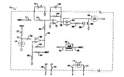
In Fig. l is illustrated a schematic diagram of
circuitry fabricated on a portion of semiconductor
substrate material lO: more particularly, the material
comprising a monolithic IC lO. The IC has fabricated
thereon, in accordance with the present invention, a
temperature sensitive semiconductor device 12, e.g., a
Gallium Arsenide (GaAs) diode 12, a semiconductor light
source 14, e.g., a GaAs laser diode l4, and a
semiconductor heating device 16, e.g., a semiconductor
resistor 16. Other well known electronic components,
some of which are described hereinafter, are fabricated
onto the substrate as well. The sensing and light
source diodes, heater and other components may all be
fabricated onto the IC substrate using known
epitaxial-diffused IC fabrication processesO
Referring to Fig. 2(a), the IC is formed by first
providing a thin layer of substrate material 20, e.g.,
GaAs, doped with a high concentration of n-type donor
.
.. . . . . . .
- :,' - ' ' -: . . ~ . .
' ' ' : ' - ~` . ' " ' : '
.
l-~v092~9014 2 ~ 9 ~ ~ ~ PCT/USg~J0~97~
atoms (i.e., atoms havin~ excess free electrons), one
side of the layer 20 being lapped and polished. Next,
an epitaxial growth procPss is used to grow a second
layer 22 on the substrate 20. The epitaxial layer 22
has a different type or concentration of impurity
atoms, e.g., a lower concentration of n-type impurity
atoms.
In the epitaxial growth process, the substrate is
exposed to a high temperature gaseous environment; the
gas containing the substrate crystal material having a
different concentration or different type vf impurity
material. The crystal material in the gas is deposited
on the polished side of the substrate. An oxide layer
24 is then formed on the epitaxial 22 layer by exposing
the IC to a high temperature oxygen or steam
atmosphere.
Re~erring to Fig. 2(b), an etching and diffusion
process is performed where sections 26 of the oxide
layer 24 are removed. Next, isolation diffusion takes
place by exposing the assembly to an atmosphere
containing the same impurities as the substrate
impurities. The time and temperature of exposure is
controlled to allow the impurities to penetrate the
epitaxial layer and reach the substrate 20, thereby
forming isolation regions 28 which allow electrical
isolation between different circuit components.
A new oxide layer 24 i5 then formed and sections
30 of the layer are removed (Fig 2(c)) to form the -
circuit components 32 (e.g., the sensing and light
source diodes 12,14 and heater resistor 16). Component
formation is accomplished using the aforementioned
isolation diffusion process with a variety of diffusion
atoms, such as n-type donor atoms or p-type acceptor
.-. . . . ..
- : . . : ~ . .
. ~
-. , , .. : ., . , .. - ,: :,- .
- ~ . . -
- . - ~ :
WOg2/19014 PCT~US92~0~97~
~,~96~3~ 8
atoms (i.e., atoms having excess free holes), to form
the desired circuit components.
In addition to oxide layer formation and
subsequent removal for i-cola~ion di~fusion, sections of
oxide layer may be removed for formation of additional
epitaxial growth layers 34, as illustrated in Fig.
2(d).
once the diffusion and epitaxial growth steps are
complete, a new oxide layer 24 is formed, and s~ctions
of the layer are again removed for deposition of metal
to form ohmic contacts 36 tFig. 31 with the components
formed in the assembly. In Fig. 3 is illustrated the
completed IC.
~eferring again to Fig. l, a DC power supply ~not
shown) external to the IC lO provides plus t+) and
minus ~-) DC Volts t+V, -V) on lines 40,42 to the
circuitry inside the IC. The light source 14 typically
comprises a laser diode and is connected by signal
lines 44 to known driver circuitry tnot shown) external
to the IC. The driver circuitry, which forms no part
of the present invention, provides the appropriate
current for proper diode operation. Alternatively, the
light source driver circuitry may, if desired, be
fabricated on the IC. +V is also provided to a
raference voltage generator 46, e.g., a zener diode,
which generates a stable voltage, VREF, on a line 48
~or use by other components on the IC.
VREF supplies a junction current ~ij) to forward
bias the sensing diode 12. The junction current flows
from VREF through a resistor 50 and the diode 12 to
ground. The Yalue of the resistor 50 connected between -
VREF and the diode is selected so that the junction
,~092/19014 PCT/US92/02972
~" 2 ~ 9
current (ii) is greater than the sensing diode
saturation current (Is).
A sensing voltage (V~) is the voltage across the
sensing diode at the junction (node) 52 between the
sensing diode and the resistor 50, and is a function of
junction current (ij) and sensing diode temperature
(T~, as given by:
Vs = (kT/q)(ln(ij/Is)) (Eq. l)
where k is Boltzmann's constant and q is the charge of
an electron.
Fig. 4 is a qraph of voltage, Vs, versus
temperature, ~, for a GaAs diode having a lO micro-amp
junction current. The relationship is approximately
linear in the temperature range of 25OC to 300 c, and
is given by:
T = 434.65~C - (444.42~C/volt)(Vs) (EqO 2)
Thus, by knowing the voltage across the sensing diode,
the temperature of the diode may be calculated.
Further, because the diode is fabricated on the
substrate, the temperature of the diode represents the
temperature of the substrate.
Referring again to Fig.-l, a non-inverting
terminal of a first operational amplifier (op-amp) 56
is connected to the node 52 through a resistor 58. A
shunt resistor (Rs) 60 is connected between an
inverting terminal of the op-amp 56 and ground. A
feedback resistor (Rf) 62 is connected between the
inverting terminal and an output terminal o~ the
op-amp. An offset resistor (Ro) 64 is connected
- ~ -
- . : . . . .. . . .
,.
- . . ., .. ~ . . .
.
.
~V0~2~9~ PCT/~S9~rO2~72
~ a9~ a~ 1O ~
between the inverting terminal and VREF to cancel any
nominal sensing diode offset voltage.
The sensing voltage (Vs) is applied at the
non-inverting terminal. ~n output voltage (VO)
generated at the output terminal is a function o~ Vs,
Rf, Rs, Ro~ and VREF as given by:
Vo = VS*~l+R~(Rg~Ro)/~Rs*Ro)] - VREF(Rf/Ro) (Eq- 3)
Thus, V0~ which is an amplified version of Vs~ is
indicative of the tempe.rature o~ the substrate as
sensed by the sensing diode. VO is supplied on a line
66 through a r~sistor 68 to an inverting terminal of a
second op-amp 70 con~igured as an error amplifier.
Additional resistors 72,74 on the IC, along with an
adjustable resistor 76 external to the IC, provide a
voltage indicative of a constant desired IC
temperature. The second op-amp 70 compares the desired
voltage (temperature) with the sensed voltaga, VO'
(temperature) and provides a signal indicative of any
difference therebetween on a line 78 to a third op amp
20 80. The second op-amp 70 has a capacitor 82 external
to the IC connected across the op-amp output and
inverting input, and connected in paxallel with an
internal resistor 84. The external capacitor 82 serves
as a filter capacitor to set the loop response.
The output of the third op-amp 80 is connected
through a resistor 86 and diode 88 to a transistor 90.
In turn, the transistor 90 is connected to the heater
resistor 16. Together, the third op-amp 80, the
resistor 86, diode 88 and transistor 90 serve as a
simple linear heater driver. In this exemplary
embodiment of the present invention, the efficiency of
.... - ~ :
. .
- - .~.- ~ ,,
~0 g2~1~14 ~ D 9 6 ' 1 ~3 P~US92~2?72
!"".
the heater driver is not a factor since the heater
driver is fabricated on the same IC as the heater 16;
hence, it can be considered a part of the heater.
During operation, a bias current signal energizes
the laser diode 14. The temperature of the laser
changes as it is operated, thereby changing the
wavelength of the light emitted by the laser. As
described hereinbefore, the changing laser wavelength
may have adverse consequences ~or high accuracy
davices. The temperature o~ the substrate changes in
response to changes in the laser temperature. The
sensing diode 12 is responsive to these changes in
laser temperature and the error amp 70 indicates the
difference between actual and desired temperaturesO
The error amp commands the heater driver, which drives
the heater 16 to heat the substrate lo until the sensed
substrate temperature equals the desired constant
substrate temperature. The response time of the
sensing diode and heater to changes in substrate
~o temperature is significantly faster than the
aforementioned prior art schemes since the laser, the
sensing diode, and the heater are fabricated on the
same substrate, thereby reducing the thermal resistance
between the el~ments.
It is to be understood that the aforementioned
circuitry fabricated on the IC is purely exemplary; any
other circuitry may be used, if desired, for sensing
the temperature of the substrate as provided for by the
sensing diode, for comparing the sensed temperature
with the desired temperature, and for driving the
heater in response thereto.
Referring to Fig. 5, an alternative embodiment of
the present invention is illustrated in which the
- , ~ . - ........................ . . .
- - . . ........... ... . ~: . .: .... : - ,
. ~. - ...... ~.. ~ .. . .
: . ,
WO92/19014 PCT/~S~ 2~72
~..,;.
~ 9 ~ 12
sensing diode 12, laser diode 14, and the heater
re~istor 1~ are fabricated on the IC 10, while any
controlling circuitry is external to the IC. As with
Fig. 1, external laser control circuitry is not
illustrated since this circuitry is well known and
forms no part of the present invention.
current through the sensing diode is provided on a
pair of signal lines 100,102 by a current source 104~
which is illustrated in detail in Fig. 7 and descr:ibed
hereinafter with reference thereto. The sensed voltage
across the sensing diode is ~ed on the lines 100,102 to
a buffer amplifier 106, which may comprise one or more
op-amps arranged in the well known instrumentation
amplifier configuration. The buffer output voltage is
indicative of the sensed substrate temperature. The
buf~er output is fed on a line 108 to an analog to
digital converter 110 (ADC3 which converts the analog
buffer output voltage to a corresponding digital
signal. Also fed to the ADC, as well as to the current
source, is a stable reference voltage, V~EF, provided
by, e.g., a zener diode 112 in a similar manner to that
of Fig. 1.
The output of the ADC 110 is provided on a set of
signal lines 114 (i.e., data bus) to a known
microprocessor 116 (UPROC). The UPROC 116 converts the
digital voltage signal into a corresponding temperature
signal using a look-up table which m~y contain a
graphical relationship between voltage and temperature
similar to that of Fig. 4. The look-up table may
comprise a plurality of memory or register locations
within the UPROC or in external memory (not shown) for
storing corresponding temperature signal informationO
~092~190~4 PCrJUS92/0297~
2 ~
13
Also input on a lin~ 118 to the UPROC is a signal
indicative of a desired constant substrate temperature.
The signal may be generated from other circuitry (not
shown), which may be responsive to other parameters in
arriving at a desired substrate temperature. The UPROC
compares the desired and sensed substrate temperatures
and provides a signal indicative of any difference
therebetween on a line 120 to heater driver cirauitry
122. The signal to the heater driver 122 may be a
pulse width modulated (PWM) signal to minimize wasted
power in the heater driver~ The heater driver may
comprise a simple transistor responsive to the PWM
signal for driving the heater with the pair of signal
lines 123 accordingly so as to closely match desired
and sensed substrate temperatures, thereby reducing
temperature-induced laser wavelength variations.
Also included may be current control circuitry 124
for the current source 104. The circuitry 124 may
comprise a known digital to analog converter 124 (DAC).
The DAC is responsive to a signal on a line 126 from
the UPROC and provides a signal on a line 128 to the
current source, as illustrated in greater detail in
Fig. 7. VREF is also fed to the DAC.
Specifically, the UPROC may contain a modelling
algorithm for the sensing diode 12. As a result, the
UPROC may adjust, through the DAC, the current source
output for proper operation of the sensing diode,
depending on the particular diode used. or,- the UPROC
may adjust the current source output to compensate for
unit to unit variations in sensins diodes.
Referring to Fig. 6, another alternative
embodiment of the present invention is illustrated in
which only the laser diode 14 and a heater resistor 16
., - . - . . . . .-. , ~ .
- : ' .' . - ~. . :
'' ' . ' ': , .
WO9~/lgO14 ~965~ PCT/US9~0297~
are fabricatad on the IC 10, while any controlling
circuitry is external to the IC. Howev2r, it is to be
understood that, in this alternative embodiment, a
portion or all of the controlling circuitry may be
fabricated on the IC, if desired. The controlling
circuitry is similar to that of Fig. 5 in that it
comprises a similar current source 104, buffer 106/
refer~nce voltage generator 112, ADC 110, UPROC 1~6,
and heater driver 122.
However, because there is no sensing diode 12
fabricated on the IC, the controlling circuitry must
monitor the voltage across the laser as well as the
current through it. A voltage indicative of the
current generated by the current source is provided on
`15 a line 130 to one input of a multiplexer 132 (mux).
The buffer voltage output on the line 108 is fed to a
second input of the mux 132. The mux alternately
chooses one of the two inputs to pass through to th2
mux output on a line 134. The mux output is fed to the
ADC, which provides the digital value of the mux output
to the UPROC.
Software inside the UPROC contains a well known
detailed model of light source temperature versus light
source current and voltage, similar to the graph of
Fig. 4. From this model the UPROC calculates the
temperature of the laser diode, and thus, the
temperature of the substrate. The UPROC compares the
calculated actual light source temperature with the
desired temperature provided on the line 118 and
provides a signal indicative of any difference
- therebetween on the line 120 to the heater driver 122.
The heater driver then co~mands the heater with
appropriate signals on the pair of lines 123 to heat
~,
~O9~J19014 PCT/US92~297~ 11
i ~"` " 2 ~ 3 .~
15
the substrate accordingly to match actual and desired
substrata temperatures.
Tha current through the laser may be controlled by
the UPROC as part of a separate control loop. The
control loop may operate on a sensed laser parameter
such as optical intensity or wavelength. The sensed
parameter (sensor not shown) is input to the UPROC on a
line 140. Software inside the UPROC calculates a
commanded laser operating current in response thereto
and provides a signal indicative thereof on the line
126 to a light source control circuit 124. The circuit
may comprise a DAC 124, similar to that of Fig. 5,
responsive to the commanded current on the line 126 in
controlling the current supplied to the laser in the
current source. VREF is also fed to the DAC.
In Fig. 7 is illustrated in more detail the
current source 104 of both Figs. 5 and 6. A fixed
resistor 150 and a variable resistor 152 are connected
between VREF and ground and provide a voltage
indicative of a desired laser operating current on a
line 154 to a non-inverting input of an op-amp 156
The output of the op-amp is connected through a
resistor 158 to a transistor 160. The collector of the
transistor 160 is pulled up to +V through a resistor
162. The emitter of the transistor is connected by the
line 100 to the anode of either the sensing diode 12
(Fig. 5~ or the laser diode l4 (Fig. 6). The cathode
of either device 12,14 is connected by the line 102 to
the inverting input of ~he op-amp 156, such input also
being connected through a resistor 164 to ground.
For the mux 132 of Fig. 6 only, the non-inverting
op-amp input is also connected to a non-inverting input
of a second op-amp 166. The second op-amp 166 is
.. . . . .
.-
- : . :
W092/1gO~4 PCT/U~ 7~ 1
?,~965~
16
configured as a voltage ~ollower, and its output is fed
on the line 130 to the mux of Fig. 6. Further, the
laser current control output on the ~ine 128 from the
DAC 124 of Figs. 5 and 6 is fed through a resistor 168
to the non-inverting input of the first op-amp 1560
In operation, current source operat.ing current is
indicated by the voltage at the non-inverting input of
the first op-amp 156. This voltage is trimmed as
necessary by the UPROC 116 through the DAC 124. The
op-amp output is converted to a current through the
transistor 160, the current being used to control
either the sensing diode 12 of Fig. 5 or the laser
diode 14 of Fig. 6.
Although the invention is illustrated with the
temperature sensor 12 implemented as a diode fabricated
on the IC, other temperature sensitive semiconductor
devices may be fabricated thereon without departing
from the spirit and scope of the present inventionO
zener diode, a semicondùctor resistor, and the
base-emitter or base-collector junction of a transistor
are examples of semiconductor devices having suitable
temperature characteristics.
Also, it is to ~e understood that the GaAs laser
diode 14 used as the semicondu~tor light source is
2~ exemplary; other light sources may be used; e.g., a
light emitting diode (LED), an edge-~mitting diode
(ELED)-, a super luminescent diode (SLD), or a
distributed feedback (DFB) laser diode.
Further, the semiconductor resistor used as the
heater 16 i~ exemplary; other heaters may be used:
e.g., a semiconductor diode or a zener diode. If
fabricated other than as a semiconductor resistor, the
heater driver circuitry must be changed from that
~09~19014 PCT/US92/02972
~- 209~t~1~
17
illustrated herein so as to match the charact~ristics
of the heater implementation.
The UPROC is described as converting the digital
voltage signal into a temperature signal using a
look-up table. However, other signal conversion
methods could be used such as a subroutine which
performs a calculation using a relationship which
deflnes the curve of the light source voltage versus
temperature characteristic. In addition, although the
the IC is described aæ being fabricated using the
epitaxial-diffused fabrication process, other
integrated circuit fabrication tech~iques could be
employed; e.g., crystal growth techniques and alloy or
fused construction.
Although the invention bas been illustrated and
described with respect to exemplary embodiments
thereof, it should be understood by those skilled in
the art that the foregoing and various other changes,
omissions and additions may be ~ade therein and
thereto, without departing from the spirit and scope of
the invention.
I claim:
. ~ ............................ .
- :: - ~ , : - ,