Note: Descriptions are shown in the official language in which they were submitted.
CA 02096~49 1999-03-16
The present invention relates to a fire detector, and
more particularly to a photoelectric-type fire detector
capable of photoelectrically detecting smoke generated as a
result of a fire, as well as to a heat-photoelectric-type
fire detector which detects occurrence of fire by sensing
both heat and smoke generated by the fire.
In the conventional photoelectric smoke detector, when
smoke arises due to fire, the light emitted from a smoke
detecting light-emitting element of a light-emitting
lo section is scattered by the smoke and enters a smoke
detecting light-receiving element of a light-receiving
section. The scattered light received by the light-
receiving element is then amplified in an amplifying
circuit and then sent to a fire-discriminating section
where fire discrimination is made on the basis of the
output value. If it is determined that there is fire, the
discriminating section transmits a fire signal to a fire
signal transmitting section through an accumulating
circuit, and the transmitting section sends this fire
signal to a fire receiver etc. for reporting on the fire.
In the conventional photoelectric-type smoke detector,
the sensitivity of the detector is adjusted by a
sensitivity adjusting means and the operation of the fire-
discriminating section etc. is stabilized by means of a
constant voltage circuit. Further, in such a type of
CA 02096S49 1999-03-16
detector, a pulsed output of an oscillating circuit is
supplied to an operation indicating lamp so that the lamp
is intermittently turned on to indicate that the detector
is operating normally.
In the conventional sensitivity adjustment, a
reflecting plate, which would generate a scattered light
being equivalent to the scattered light which would be
generated when 10%/m of smoke has entered, is disposed in a
smoke detecting dark box of the photoelectric-type smoke
o detector, and a detected output at that time is used for
selecting a reference resistance of a comparator as a fire
discriminating means such that the comparator replies. As
a result, the detected output would become varied due to
the dispersion of the circuit constant of an electric
circuit of the respective photoelectric smoke detector.
This leads to a troublesome procedure for the sensitivity
adjustment i.e. the selection of the reference resistance.
In addition, since a different value of the detected output
is obtained in each of the photoelectric-type smoke
detectors, in order to know the historical variation of the
sensitivity of the detector from the initial state, the
initial detected outputs of the detectors must be
recognized.
The conventional detector includes an accumulating
circuit composed of a plurality of D-type flip-flops.
~... ...
.. ... .... ..
.........
CA 02096~49 1999-03-16
Accordingly, for example, the fire signal would be
sometimes undesirably transmitted from the fire signal
transmitting section by the operation of the accumulating
circuit upon turning on of the power source when the fire
resetting operation is carried out.
The constant voltage circuit in the conventional
detector is composed of a transistor, a Zener diode
connected to a base of the transistor, and a resistor
connected between a collector and the base of the
lo transistor. Therefore, when there is a significant
difference in the power source voltage to be supplied to
the smoke detector between the fire receivers, the current
to be consumed in the constant voltage circuit of the smoke
detector would become varied depending on the fire receiver
to be connected. For example, when the power source
voltage is high, the current flowing through the Zener
diode of the constant voltage circuit would become
correspondingly large, while when the power source voltage
is low, the current flowing through the Zener diode of the
constant voltage would become correspondingly small.
Thus, in the case of a fire receiver with a high power
source voltage to be supplied to the smoke detector, there
is such a disadvantage that the number of the smoke
detectors which can be connected is significantly
restricted due to the power consumption of the constant
. CA 02096S49 1999-03-16
voltage circuit, in comparison with a fire receiver with a
low power source voltage. Further, the power source
voltage of the fire receiver is sometimes unstable and
fluctuates. In such a case, if the fire detector is
changed to a smoke detector having semiconductor circuits,
a necessary number of fire detectors cannot be connected.
In the conventional detector, the oscillating circuit
of the operation indicating lamp is provided separate from
and independent of a pulse oscillating circuit for
lo supplying the pulsed output to the smoke detecting light-
emitting element of the light-emitting section. As a
result, even if the pulse oscillating circuit for detecting
the smoke fails so as not to make the light-emitting
element emit light i.e. in a fire-monitoring unable state,
the indicating lamp flickers if the oscillating circuit is
normally operable, erroneously indicating that the detector
is in normal state.
The invention provides a fire detector which is
capable of readily and accurately adjusting the sensitivity
and of not erroneously outputting any fire signal. This
invention also provides a fire detector which is capable of
making the current consumption of a constant voltage
circuit unchanged and of accurately indicating operation.
According to a first aspect of the invention a
photoelectric-type fire detector comprises: a light-
CA 02096~49 1999-03-16
emitting section for emitting a pulsed light for detecting
smoke; a light-receiving section for receiving scattered
light of the pulsed light emitted from the light-emitting
section caused by smoke, and an amplifying section for
amplifying an output from the light-receiving section to
generate a light-receiving output, the amplifying section
having a first variable resistor for adjusting the light-
receiving output to a predetermined value in a state in
which there is an absence of smoke; a smoke-discriminating
lo section having a second variable resistor for adjusting a
reference voltage, for generating a smoke-discriminating
output when the light-receiving output from the light-
receiving section reaches the reference voltage; and a fire
signal transmitting section for transmitting a fire signal
based on the smoke-discriminating output from the smoke-
discriminating section.
Preferably, the detector can include an accumulating
circuit for judging whether any smoke-discriminating output
has been output from the smoke-discriminating section in
synchronism with the pulsed light from the light-emitting
section, and for outputting a detecting output when it is
judged that smoke-discriminating outputs have been output
for a predetermined number of times. The fire signal
transmitting section transmits the fire signal in response
to the detected signal from the accumulating circuit.
~ - CA 02096~49 1999-03-16
A photoelectric-type fire detector according to
another aspect comprises: a light-emitting section for
emitting a pulsed light for detecting smoke; a light-
receiving section, having a first variable resistor for
setting a light-receiving output from the light-receiving
section to a predetermined value in the presence of smoke
of a predetermined density, the light-receiving section
receiving scattered light of the light emitted from the
light-emitting section caused by smoke; a smoke-
o discriminating section, having a second variable resistorfor adjusting a reference voltage, for generating a smoke-
discriminating output when a light-receiving output from
the light-receiving section reaches the reference voltage;
a fire signal transmitting section for transmitting a fire
signal based on the smoke-discriminating output from the
smoke-discriminating section; and a constant voltage
circuit for converting an externally supplied power source
voltage into a predetermined voltage and for supplying the
converted voltage to the light-emitting section, the light-
receiving section and the smoke-discriminating section.
A photoelectric-type fire detector according to a
third aspect comprises: a light-emitting section for
emitting a pulsed light for detecting smoke; a light-
receiving section for receiving scattered light of the
pulsed light emitted from the light-emitting section caused
.
. CA 02096~49 1999-03-16
., .
by smoke, and an amplifying section for amplifying an
output from the light-receiving section to generate a
light-receiving output, the amplifying section having a
first variable resistor for adjusting the light-receiving
output to a predetermined value in a state in which there
is an absence of smoke; an A/D converting circuit for
converting the light-receiving output from the light-
receiving section into digital signals; and a signal-
transmitting section for transmitting the digital signal
lo converted in the A/D converting circuit.
According to a fourth aspect the invention provides a
heat-phôtoelectric-type fire detector comprising: a light-
emitting section for emitting a pulsed light for detecting
smoke; a light-receiving section for receiving scattered
light of the pulsed light emitted from the light-emitting
section caused by smoke; a smoke-discriminating section for
providing a smoke-discriminating output when a light-
receiving output from the light-receiving section reaches a
reference voltage; a heat-sensitive element for detecting
heat; a heat-discriminating section for providing a heat-
discriminating output when a detected output from the heat-
sensitive element reaches a predetermined level; and a fire
signal transmitting section for transmitting a fire signal
when a smoke-discriminating output or a heat-discriminating
output is output from at least one of the smoke-
~ CA 02096~49 1999-03-16
discriminating section and the heat-discriminating section.
The detector can include a constant voltage circuit for
converting an externally supplied power source voltage into
a predetermined voltage, and for supplying it to the light-
emitting section, the light-receiving section, the smoke-
discriminating section and the heat-discriminating section.
A heat-photoelectric-type fire detector according to a
fifth aspect comprises: a light-emitting section for
emitting a pulsed light for detecting smoke; a light-
lo receiving section for receiving scattered light of thepulsed light emitted from the light-emitting section caused
by smoke, and an amplifying section for amplifying an
output from the light-receiving element to generate a
light-receiving output, the amplifying section having a
first variable resistor for adjusting the light-receiving
output to a predetermined value in a state in which there
is an absence of smoke; a heat-sensitive element for
detecting heat; a heat-discriminating section for
generating a heat-discriminating output when a detected
output from the heat-sensitive element reaches a
predetermined level; an A/D converting circuit for
converting the light-receiving output from the light-
receiving section and the detected output from the heat-
discriminating section into digital signals; and a signal-
CA 02096~49 1999-03-16
transmitting section for transmitting the converted digital
signal from the A/D converting circuit.
Embodiments of the invention now will be described,
with reference to the accompanying drawings in which:
FIG. 1 is a circuit diagram showing a photoelectric-
type fire detector according to a first embodiment of the
present invention;
FIG. 2 is a circuit diagram showing a photoelectric-
type fire detector according to a second embodiment of the
present invention;
FIG. 3 is a circuit diagram showing an accumulating
circuit according to a third embodiment of the present
invention;
FIG. 4 is a circuit diagram showing a fourth
embodiment of the present invention; and
FIG. 5 is a circuit diagram showing a fifth em~bo~;ment
of the present invention.
FIRST EMBODIMENT
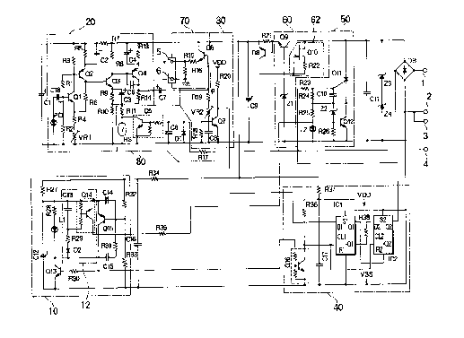
In FIG. 1, a photoelectric fire detector according to
a first embodiment comprises a light-emitting section 10, a
light-receiving section 20, a fire discriminating section
30, an accumulating section 40, a fire signal transmitting
section 50, a constant voltage circuit 60, a sensor output
circuit 70 and a
~ 2 0 ~6 549
test circuit 80.
The ligbt-emitting section 10 includes a smoke
detecting light-emitting element (a light-emitting diode) L1,
transistors Q13 - Q15, resistors R27 - R33, capacitors C1Z -
C15, ~d a diode D2. In this light-emitting section 10, the
transistors Q13, Q15, the resistors R27, R28, R30 - 33, and the
c~r~~;tors C12, C14, C15 form an osc;~1~ting circuit for
supplying a pulse ou~u~ to the light-emitting element L1.
The transistor Q14, the resistance R29, the cAp~citor
C13 and the diode D2 form a pulse width exr~n~ing circuit 12.
This pulse width exp~n~;ng circuit 12 ~Xp~n~C the pulse width of
the pulse Ou~u~ of the os~ ting circuit and supplies it to
an operation indicating lamp L2 of the fire signal transmitting
section 50.
The light-receiving section 20 includes a smoke
detecting light-receiving element (a photo-diode) PD,
transistors Q1 - Q4, resistors R1 - R10, R13, R14, an output-
adjusting variable resistor VR1 and capacitors C2 - C5, C18.
The light-receiving element PD does not directly receives the
light emitted from the light-emitting element L1, but receives
the l-ight scattered by smoke.
The transistors Q1, Q2, the resistors R1 - R6, the
o~u~-adjusting variable resistor VR1, and the c~r~itors C2,
C18 form a first-stage amplifying circuit. This amplifying
circuit amplifies the ~'u~u~ of the light-receiving element PD,
-10-
2~)9~i~49
while the variable resistor VR1 is a first sensitivity-adiusting
variable resistor as a feedback resistor for the amplifying
circuit.
The transistors Q3, Q4, the resistors R8 - R10, R13,
R14, and the car~c; tors C3 - C5 form a second stage amplifying
circuit. This amplifying circuit further amplifies the ou~u~
of the first-stage amplifying circuit.
The fire discriminating section 30 includes a
transistor Q7, resistors R18 - R20, a reference voltage
adjusting v ~iable resistor VR2 and a cAr~citor C8. The
variable resistor VR2, the secQnd fixed resistor R18 and the
fiEst fixed resistor R19 form a divisional resi~ ce circuit
(series resistance circuit).
m e variable r~esistor VR2 is a cec~n~ sensitivity
adjusting variable resistor to which the amplified ou-y~- from
the light-receiving section 20 is supplied. The transistor Q7
has a base and an emitter cQnnected to both ends of the sec~
fixed resistor R18 and is a fire discriminating transistor being
t~rned on and off by a divisional voltage of the divisional
resistance circuit.
The accumulating circuit 40 includes a transistor Q16,
a resistor R36, a ~ulLe~ limiting resistor R37, a resistor R38,
a ca~citor C17 and D-type flip-flops IC1, IC2. An ou~u~ from
the transistor Q7 of the fire discriminating section 30 and an
o~ L from the osc; 11 ~ting circuit of the light-emitting
-11 -
20~fi549
section are connected to the accumulating circuit 40.
The accumulating circuit 40 discriminates in
synchronous with the pulse ou~u~ from the osci11~ting circuit
of the light-emitting section 10 whether the transistor Q7 of
the fire discriminating section 30 has been turned on plural
times, and outputs a detected output if the discriminated result
is affirmative. The ~ and - power source terminals of the
flip-flop IC1 and IC2 are co~ ed to VDD and VSS
respectively.
The fire sign~1 transmitting section 50 includes a
silicon CO11LLO1 rectifying element Q11, a transistor Q12, an
o~eL~Lion indicating lamp L2, a Zener diode Z2, resistors R23 -
R26 and a capacitor C10. The rectifying element Q11 is turned
on by the detected output~of the accumulating circuit 40, and is
connected in series with the operation indicating lamp L2.
The transistor Ql 2 turns on when the circuit
comprising the Zener diode Z2 and the resistor 26 has detected a
rise of the voltage applied to the operation indicating lamp L2
to a pLede~ermined value so as to prevent a voltage excee~;ng
the ~LedeLermined voltage from being applied to the operation
indicating lamp L2-.
The constant voltage circuit 60 includes a transistor
Q9, a junction-type field effect transistor (FET) Q10, a
resistor R22 and a Zener diode Z1. The constant voltage circuit
60 supplies a power to the light-emitting section 10, the light-
-12~
2096549
receiving section 20, the fire discriminating section 30 and the
accumulating circuit 40.
The transistor Q9 has a constant ~uLLen~ circuit 62
between its collector and base, while the Zener diode Z1 is
csnnected between the base of the transistor Qg and the earth
terminal. The constant ~ullellL circuit 62 is composed of a
junction type ~-r Q10 having a drain connected to the collector
of the transistor Q9 and a gate conn~cted to the base of the
LL~istor Q9, and a resistor R22 connected between the source
and the gate of the transistor Q10.
The sencor o~u~ circuit 70 includes a transistor Q6
and resistors R15, R16. The base of the transistor Q6 is
conn~cted to the connecting point P of the o~ end of the
light-receiving section 20 and the division~l resistance circuit
of the fire discriminating section 30, and the emitter thereof
being earthed through the output resistors R15 and R16.
The test circuit 80 includes a transistor Q5 as a
switching element, a c~p~;tor C6, resistors R11 and R17, a
diode D1 and a reed switch RS closing in response to an dp~.oach
of a magnet. The switching element Q5 is conn~cted in parallel
with a reed switch RS. The parallel circuit of the reed switch
RS and the switching element Q5 is aL.~ ~ed in parallel with the
gain ~o~ olling resistor R10 of the -~econd-stage amplifying
circuit of the light-receiving section 20.
A non-polarizing diode bridge circuit DB is provided.
-13-
2~)9~5 4 9
The Zener diodes Z3, Z4 and the capacitor Cll form an absorbing
circuit for a surge voltage. The terminals 1, 2 and 3 are for
coupling a pair of power-source/signal lines not shown, and the
terminal 2 and 3 are short-circuited to connect selectively one
power-source/signal line in the detector.
The terminal 4 is an input terminal of the test signal
(test voltage), while the terminals 5 and 6 are for uu~u~ing
an analog light-receiving output of the light-receiving se~tion
20.
The operation of the detector according to this
embodiment will now be described. For example, when a power
sou~ce is turned on to supply power to the detector after
restoration from fire, the c~p~c;tor C17 for supplying
operational power to the flip-flop IC1 and IC2 in the
accuml11ating circuit 40 is charged through the ~ULL~ limiting
resistor R37 with a time constant of ~ = R37 X C17, and the
voltage between both ends of the c~p~itor C17 is applied to the
flip-flops IC1 and IC2.
At the time of tllr~; ng on of the power source, the
flip-flops IC1 and IC2 are unstable and provide two kinds of
states: one, an L vu~u~ is generated from the output end Q2 of
the flip-flop IC2, i.e. no o~u~ signal; and the other, an H
o~L~u~ is generated from the output end Q2 of the flip-flop IC2,
i.e. o~u~ sig,ilal present.
When the o'u~u~ end Q2 of the flip-flop IC2 is L
2 0 9~5 ~ 9
output, the capacitor C17 is directly charged to a predetermined
voltage. On the other hand, when the output end Q2 of the flip-
flop IC2 is H output, an H ou~u~ with a ~ullell~ value limited
by the ~u..~n~ limiting resistor R37 is generated from the
ou~u~ end Q2. Therefore, since the current necessary to turn
on the~silicon control rectifying element Q11 is not supplied to
its gate through the flip-flop IC2, this element Q11 is not
activated. At this time, the capacitor C17 is charged up to a
voltage determined by the current limiting resistors R37 and the
resistors R23, R24 and R25.
The capacitor C12 of the light-emitting section 10 is
charged, via the resistor R27, with a power supplied from a fire
receiver (not shown) or a transmitter through the terminals 1
and 2 or 3. When the charging voltage re~hsc a summed voltage
of the divisional voltage by the resistors R32 and R33 and the
base-emitter voltage V~ E of the transistor Q15 (hereinafter
referred to as a light-emitting reference voltage), the
transistor Q15 and correspondingly the transistor Q13 turn on.
When the transistor Q13 turns on, the c~r~c;tor C12 is
~icr-h~rged through the resistor R28 and the smoke detecting
light-emitting element L1 which then emits light, and the
transistor Q14 turns on. At the same time, this ~;Cch~rging
~u..~ makes the capacitor C13 be charged.
The turning on of the transistor Q15 makes the
transistor Q16 of the accumulating circuit 40 turn on, and clock
-15-
~ ~ ~6'~ 9
signals are supplied to the ~lip-flops IC1 and IC2 as light
emission synchroni~;ng signals. The time during which the
transistor Q13 of the light-emitting section 10 is turned on
corresponds to the time during which the capacitor C15 is
charged with the base ~uLle-l- of the transistor Q15 and due to
this charged voltage the transistor Q15 is turned off. This
time is selected, for example, to provide the light emission for
100~ cecon~C at an interval of three .secon~c.
The transistor Q14 tllrns on by the ~-cr-h~rging ~uLLel~t
of the c~rac;tor C12 w-hile the transistor Q13 is tllrn~A on. m e
tl~rn;ng off of the trancistor Ql 3 stops the charging operation
for the c~p~itor C13, which then ~ h~rges through the
resistors of the transistor Q14 connected in parallel therewith.
The transistor Ql 4 is ~ kept turned on by this ~;crh~rging
~; UL L ~311(. .
The transistor Q14 in the t~lrnp~ on state supplies the
charges on the c~p~c;tor C14, as an operational power, to the
~peL&~ion indicating lamp L2 of the fire signal transmitting
section 50 through the resistor R35. The tllrn;ng-on time of
this transistor Q14 is selected such that any person can
~iclt~lly recognize the turning-on of the operation indicating
lamp L2, for example 1ms.
The light-receiving section 20 detects scattered light
from the smoke detecting light-emitting element L1 with the
smoke detecting light-receiving element PD to amplify the
-16-
2 0 ~ 9
detected signal by the two-stages amplifying circuit, and
outputs the amplified signal to ~he fire discriminating section
30. When the base voltage generated by dividing the output from
the light-receiving section 20 by using the resistor R19,
reference voltage adjusting variable resistor VR2, and the
resistor R18 is lower than the base-emitter voltage of the
transistor Q7 of the fire discriminating section 30, it remains
t~rne~ off to o~y~L a high (H) signal to the accumulating
circuit 40. On the other hand, when the base voltage eycee~c
the base-emitter voltage~ the transistor Q7 turns on to o~uL a
low (L) signal as a fire discriminating signal to the
~c~umulating circuit 40.
The flip-flop IC1 of the accumulating circuit 40
provides a H signal through its output terminal Q1 and a L
signal through its inverted output terminal ~Q1 so as to reset
the flip-flop IC2, when the clock signal (synchron;7-ing sign~1
from the light-emitting section 10) is supplied to its clock
terminal CL1 from the transistor Q16 while receiving a H signal
at its input terminal D1. As a result, the ou~u~ terminal Q2
of the flip-flop IC2 provides no ou~u~ signal, such that the
capacitor C17 is recharged through the current limiting resistor
R37 up to a predetermined voltage.
When a clock signal is supplied to the clock terminal
CL2, the flip-flop IC2 supplies an L ou~u~ to the fire signal
transmitting section 50 through its output terminal Q2 in
-17-
.
~ . :
2 0 96S 4 ~
response to the L output of the inverted output terminal ~Q1 of
the fli~p-flop IC1~ Accordingly, the silicon control rectifying
element Q11 of the transmitting section 50 is kept turned off.
The flip-flop IC1 of the accumulating circuit 40
provides the L output through its output terminal Q1 and the H
ou~u~ through its inverted output terminal ~Q1, if the L signal
as the fire discriminating signal is input to the input terminal
D1 when the clock signal is input to the clock terminal CL1. On
the other hand, the flip-flop IC2 maintains the L ou~ at its
ou~u~ terminal Q2, since the inverted output terminal ~Q1 of
the flip-flop IC1 is still in L o~ state when the clock
signal is supplied to the clock terminal CL2.
In this state, if the L signal being the fire
discriminating signal is~ input again to the input terminal D1
when the clock signal is supplied to the clock terminal CL1 of
the $1ip-flop IC1, the flip-flop IC2 generates the H o~
through its output terminal Q2 in resp~ce to the H output of
the inverted output terminal ~Q1 of the flip-flop IC1.
The H ~u~u~ of the flip-flop IC2 makes the charges
having been stored in the capacitor C17 discharge as the ou-
~signals, and in response to the ~ signals of- this
~;.Cch~rging ~UlLel~ t~e silicon CW1~LO1 rectifying element Q11
of the fire signal transmitting section 50 turns on so as to
transmit the fire sign~1 through the terminals 1 and 2 or 3.
Accordingly, the operation indicating lamp L2 changes from the
-18-
Z()9fi549
intermittent lighting s~ate by the pulse outputs to the
continuous ligh~ing state by the fire signals.
During the transmission of the fire signals, if the
power source voltage supplied from e.g. the receiver fluctuates
to increase and the ~uL~en~ flowing through the series circuit
composed of the resistor R25 and the operation indicating lamp
L2 increases such that the voltage drop of this series circuit
excee~c the Zener voltage of the Zener diode Z2, the Zener diode
Z2 con~l~cts and the transistor Q12 turns on. In conceguence, it
is possihle to ~L~V~ the ~uL,en~ flowing through the operation
indicating lamp L2 from lmnece~ss~ily incre~c;ng due to the
flu~ua~ion of the power source voltage.
When the clock signal is sent to the clock terminal
CL1 of the flip-flop IC1 of the accumulating circuit 40, if the
level of the input terminal D1 has already been changed from the
L signal to the H signal i.e. the fire discriminating section 30
does not provide any discriminating output, the ou~u~ terminal
Q1 of the flip-flop IC1 changes from L ou~u~ state to the H
o~y~ state while the inverted ou~ terminal ~Q1 ch~nges from
the H output state to the L o~u~ state. Accordingly, the
flip-flop IC2 is reset and the ou~u~ terminal Q2 maintains the
L o~uL state. AS a result, even if any temporary phenomenon
makes the fire discriminating section 30 ou~u~ the
discriminating signal only one time, the accumulating circuit 40
does not provide any output and the transmitting section 50 does
-19-
,, ~
'. ''
-
2 0 9~ 54 9
not provide any fire signal.
When the power supply from the receiver etc. istemporarily shut down for resetting the operated fire detector,
tho silicon co"~.ol rectifying element Q11 rec~veLs and the
flip-flops IC1 and IC2 are set to the initial state.
In testing the fire detector for judging whether
operable or not, a test signal is input to the terminal 4 from a
not shown receiver or the like to turn on the transistor Q5 of
the testing circuit 80, or a not shown magnet is ap~Lo~hed to
the detector to turn the read switch R5 on. As a result, the
the resistor R11 of the testing circuit 80 is cq~nected in
parallel to the resistor R10 of the second-stage amplifying
circuit of the light-receiving section 20 so that the gain of
the secQnd amplifying circuit increases. Then, the amplified
~u~u~ from the light-receiving element PD due to the light
emission of the light-emitting element L1 in the case of no
smoke state would become the ou~ù~ required to operate the
transistor Q7 of the fire discriminating section 30.
If there is not any abnormalities in the light-
emitting element L1 of the light-emitting section 10, the light-
receiving element PD of the Iight-receiving section 20, and the
amplifying circuit, the fire discriminating section 30 generates
the fire discriminating ou~u-. And when the plurality of the
fire discriminating ou-~u~s are continuously generated, the
accumulating circuit 40 and the fire signal transmitting circuit
-20-
2 0 9~ 5 ~ 9
50 are activated to transmit fire signals and to change the
operati,on indicating lamp L2 to the continuous lighting state.
On the contrary, if there is any abnormality in such components
and CiI-cuits, the transmitting circuit 50 does not transmit any
fire signal and the operation indicating lamp L2 does not
continuously light.
For adjusting the sensitivity of the photoelectric
type smoke detector, a tester such as a voltmeter is ~irst
connected between the terminals 5 and 6, and -sllhsequently the
o~u~ adjusting v ~iable resistor VRl of the light-receiving
section 20 is adjusted such that the amplified ~u~u~ of the
section 20 in the state without smoke in the dark box becomes a
predetermined value. The amplified output of the light-
receiving section 20 a~t this time is equal to the output
provided,by receiving the light which is emitted from the light-
emitting element Ll and then scattered on the inner wall of the
dark box.
Next, the reference voltage adjusting variable
resistor VR2 of the fire discriminating section 30 is adjusted
such that the transistor Q7 turns on when smoke' of a
predetermined density e.g. a density of 10%/m or a reflection
plate generating light reflection equivalent thereto is ~i-sposed
in the dark box. At this time, the smoke density or the
reflection plate to be disposed in the dark box need not be a
smoke density judged as a fire or a reflection plate equivalent
.
-21-
,
, . .
, . ~
.. ' ~ ' ' ' ~ ''
-
2 0 96~ 4 9
thereto. Namely, each detector can adjust the amplified ou~u~
from the amplifying circuit to a predetermined value by
adjusting the variable resistor VRl. Accordingly, the
differ~nces in the amplified o~u~s among the detectors due to
the dispersion of the circuit components such as the light-
emitting elements Ll, light-receiving elements PD and the
amplifying circuits are corrected.
The amplified o~ is proportional to the smoke
density entering between the light-emitting element L1 and the
light-receiving element PD. Therefore, when a desired smoke
density or a reflection plate generating a reflection light
eguivalent thereto ïs used, a voltage drop corresponding to the
desired smoke density is required to generate in the resistor
R18 of the fire discriminating section 30.
Accordingly, for adjusting the discriminating level by
the reference voltage adjusting variable resistor VR2, the smoke
density in the dark box or the reflection amount from the
reflection plate equivalent thereto may be sufficient with a
desired smoke density or a reflection amount co~le~Qn~ing to
the desired smoke density, and reference voltage adjusting
variable resistor VR2 is adjusted such that a voltage drop
generated in the series resistance circuit composed o~ the
variable resistor VR2, the resistors R18 and R19 becomes the
voltage drop corresponding to the desired smoke density. As a
result, when smoke of a predetermined density discriminated as a
- 2-
2 ~ 9~i~ 4 9
fire flows into the dark box, due to the amplified output at
this time, a voltage drop necessary to turn on the transistor Q7
is generated in the resistor R18 of the fire discriminating
section 30.
The output i.e. the light-emitting amount of the
light-emitting element L1 of the light-receiving section 10
re~l~ces as the tempe a~ule increases while the base-emitter
voltage V~E of the transistor Q6 of the -~encor O~u~ circuit 70
re~tlce~ as the tempeLaLuue increases. Therefore, this
transistor Q6 acts to compensate the o~u~ reduction of the
light-emitting element Ll. Furthert the transistor Q6 functions
to expand the sensor ouLyuL by using its base-emitter voltage
V8 ~ and then outputs it to the output terminals 5 and 6. As a
result, since any slight variation of the sencqr output is
9X~n~e~ and output between the output terminals 5 and 6, it
becomes possible to readily perform the sensitivity adjustment
by the ouL~uL adjusting variable resistor VRl or the reference
voltage adjusting variable resistor VR2 and the checking of the
sensitivity variation.
The oon~ voltage circuit 60 keeps the current
flowing through the Zener diode Z1 CO~ by the constant
~u-Lel.L effect of the constant current circuit 62 composed of
the E~-l Q10 and the resistor R22, to keep the current
consumption in the constant voltage circuit 60 constant.
Therefore, any fluctuation of the power source voltage from the
.
2 ~ ~6 54 9
receiver et al. does not affect the current consumption of the
constant voltage circuit 60.
A series circuit composed of the current limiting
resistor R37 and the c~p~;tor C17 is provided in the
accumulating circuit 40 for being prevented the fire signal
transmitting circuit 50 from activating by the mis-operation of
the flip-flops IC1, IC2 at the time the power source is-turned
on. The c~ itor C17-acts to supply power to the flip-flops
IC1, IC2 to limit the ~,er.~s to be supplied to the flip-flops
IC1 and IC2 by the ~lLen~ limiting resistor R37 until the
charging voltage re~ches a predetermined value.
Con-cequently, even if the states of the flip-flops IC1
and IC2 are unstable immediately after tllrn; ng on the power
so~ce and the flip-flop IC2 generates the H output at its
ou~u~ terminal Q2, the flip-flop IC2 acts not to provide the
~ULL~ required to trigger the silicon cun~ol rectifying
element Q11.
When clock pulses (~y,w~l~Q~;7;~g signals) are supplied
from the light-emitting section 10 and the ~uL~u~ terminal Q2 of
the flip-flop IC2 is set to L ou~u~ state, the capacitor C17 is
charged up, thereby preventing any mis-operation on turning on
the power source.
With the aforementioned composition of the detector
a~coL~ing to the first embodiment of the present invention, the
following notable advantages can be obt~ine~:
-24-
2 0 ~6 ~4 9
(1) There are provided the first-stage amplifying circuit
having the output adjusting variable resistor VR1 for amplifying
the output of the light-receiving element PD, and a fire
discri~inating section 30 having a reference voltage adjusting
variable resistor VR2 to which the amplified output from the
light-receiving section 20 is supplied. As a result, it is
possible to adjust the amplified output to a predeterm;neA value
by the ou~u~ adjusting variable resistor VR1, and to adjust the
switching level of the fire discriminating section 30 to a
predetermined value by the reference voltage adjusting variable
resistor VR2.
Therefore, the sensitivity of the photoelectric smoke
detector can be readily adjusted since the amplified ou~ from
the amplifying circuit can be the same value for the
photoelectric smoke detectors while the switching level of the
fire discriminating section can be the same value for the
photoelectric smoke detectors.
Further, s nce the amplified outputs of the amplifying
circuits have the same value for the photoelectric smoke
detectors, it is possible to easily recognize the degree of the
fluctuation of the detected outputs in the no smoke state from
the initially detected GU~U~.
(2) The accumulating circuit 40 discriminates whether the
transistor Q7 of the fire discriminating section 30 has been
tl~rned on for a plurality of times succes~;vely in synchronous
-25-
2()96~ 9
with the pulse outputs from the light-emitting section 10, and
dispatches the detected output to the fire signal transmitting
section 50 when the discriminated result is a~firmative. As a
result, the fire signal transmitting section 50 would not
erroneoll~ly operate on turning on the power source.
(3) The constant voltage circuit 60 includes a transistor Q9
having the constant current circuit 62 between its collector and
base, and the Zener diode Z1 connected between the base of the
transistor Q9 and earth. Therefore, the current flowing through
the Zener diode Z1 becomes always constant by virtue of the
constant ~ re~t circuit 62 connPcted in series with the diode
Zl~ even if the power source voltage to be applied between the
collector of tne transistor Q9 and the cathode of the Z~ner
diode Z1 by the fire receiver is v ~ied. As a result,
irrespective of the value of the power source voltage, the
current consumption of the constant voltage circuit 60 becomes
~o~
(4) The light-emittin~ section 10 includes the pulse width
expanding circuit 12 for exp~n~;ng the pulse width-of the pulse
output from the osc; 11 ~ting circuit. Since the output of the
pulse width e~r~n~;ng circuit 12 is connPcted to the operation
indicating lamp L2 of the fire signal transmitting section 50,
the pulse output of the oscillating circuit for controlling the
light emission of the light-emitting element Ll is exr~n~ed by
the pulse width exr~n~;ng circuit 12, and the operation
-26-
2096549
indicating lamp 12 turns on by the expanded pulse. As a result,
it is possible to recognize any abnormality occurrence in the
detector by the lighting off of the operation indicating lamp
when the oscillation of the oscillating circuit stops.
Second Embodiment:
FIG. 2 is a circuit diagram of a heat-photoelectric
type fire detector according to a ~econ~ embodiment of the
present invention. This embodiment is composed by newly adding
a heat detecting section 90 to the detector of the first
embodiment shown in FIG. 1. The heat detecting section 90 is
cnnn~cted to the light-emitting section 10, the accumulating
circuit 40 and the fire signal transmitting section 50 for
discriminating the fire by detecting the generation of heat and
transmits a fire discriminating signal to the accumulating
circuit 40.
The heat detecting section 90 includes a heat-
sensitive element TX, comparators ICT1 and ICT2 respectively
composed of an operational amplifier, ~Lo-~istors QT1 and QT2, a
cap~;tor CT and resistors RT1 - RT11. As the heat-sensitive
element TH, a negative characteristic thermistor or the like is
used for generating an output corresponding to the physical
amount of the detected heat.
Next, the operation of the fire detector according to
this second embodiment will be described. The heat detecting
-27-
. 2 0 ~6 S4 ~
section 90 receives, as power, pulse signals having been
expanded in the pulse width expanding circuit 12 of the light-
emittin~ section 10. Then the heat detecting section 90
intermittently detects any resistance change of the heat-
sensiti~e element TH due to the temperature change, which is
monitored by the comparators ICT1 and ICT2. The comparator ICT1
is used for discximinating the fire, and provides an H output
when the input voltage of its negative-side terminal becomes
lower than the fire discriminating reference voltage of the
positive-side terminal i.e. the divisional voltage of the
resistors RT3 and RT4 due to the resistance drop by the heat of
the heat-sensitive element TH. In response to this H o~u~,
the transistor QT1 turns on and the fire discriminating signal
of L output is supplied to the flip-flop IC1 of the accumulating
circuit 40.
Although the input terminal D1 of the flip-flop IC1 of
the accumulating circuit 40 recei~es the ou~u~ from the fire
discriminating section 30 and the cutput from the transistor QT1
of the heat detecting section 90, the accumulating circuit 40
operating totally in the same manner as in the first embodiment.
Namely, when the fire discriminating section 50 discriminates
any fire by smoke, or the heat detecting section 90
discriminates any fire by heat so as to provide the fire
discriminating signal of L ou~ suc~essively two times to the
input terminal D1 of the flip-flop IC1, the H output is supplied
-28-
2 0 ~ 4 9
to the fire si~lal transmitting section S0 from the accumulating
circuit 40. Accordingly, fire signals are transmitted to a fire
receiver not shown etc. from the fire signal transmitting
section 50 and the operation indicating lamp L2 changes from the
intermittent lighting state to the continuous lighting state~
Further, in case of the heat-sensitive element TH
being snapped, when the power is supplied to the heat detecting
section 90 from the pulse width exp~n~;ng circuit 12, the
potential at the connecting point of the resistors RT2 and RT11
exceeds the reference voltage for discriminating snapping by the
divisional resistors RT5 and RT6. As a result, the H o~u~ is
provided from the comparator ICT2 to turn on the transistor QT2.
Therefore, both ends of the operation indicating lamp L2 of the
fire signal transmitting section 50 are short-circuited. In
con-ce~uence, the operation indicating lamp L2 stops the
intermittent lighting by the pulse signals supplied from the
pulse width exp~n~; ng circuit 12 of the light-emitting section
to indicate occurence of abnormalities. The operation
indicating lamp L2 also stops lighting when neither the smoke
detection nor the heat detection can be carried out by the
stopping of the oscillation of the oscillating circuit of the
light-emitting section 10, from which one can reco~n;7-e the
oc~uL~nce of any abnormalities in the detector.
- The other functions are the same as in the first
embodiment.
-29-
2 0 ~6~ 9
In this second embodiment, the output from the
oscillating circuit in the light-emitting section 10 having been
expanded to be a pulse signal having a width of ~Lu~imately
1ms in the pulse width exp~n~;ng circuit 12 is supplied to the
heat detecting section 90 as the operational power.
Alternatively, it is also possible, when it is lmnecesC~ry to
intermittently light the operation indicating lamp L2, to supply
the pulse signal having a width of a~Lo~imately 100 ~s ou~
from the osç; 11 ating circuit in the light-emitting section 10
directly to the heat detecting section 90.
As mentioned above, accûL~ing to the second embodiment
of this invention, since the pulse signals from the o.s~ ting
circuit of the light-emitting section 10 is shunted and supplied
to the heat detecting sectlon 90 as the power, the heat is
intermittently detected. Accordingly, the poWer consumption by
the heat detecting section 90 is reduced, and any osc~ ting
circuit for detecting heat need not be provided se~aL~ely.
Third Embodiment: .
The accumulating circuit 40 used in the previous
embodiments 1 and.2 is a two-stages type accumulating circuit
composed of serially connected two D-type flip-flops IC1 and IC2
which provides the uu~u~ signal to the fire signal transmitting
section 50 when the fire discriminating ou~ s ~ e provided
c~lccess;vely two times from the fire discriminating section 30
-30-
2 0 ~;5~ 9
or the fire discriminating section 30 and the heat detecting
section 90. Alternatively, however, it is also possible to use
a three-stages type accumulating circuit 40a composed of three
D-type flip-flops IC1, IC2 and IC3 coupled as shown in FIG. 3.
In this case, the output from the accumulating circuit 40a is
supplied to the fire signal transmitting section 50 when the
fire discriminating section 30 generates the fire discriminating
ou~u~ c~lccess;vely three times.
Fourth Embodiment:
In the first and the secon~ embodiments, the firc
discriminating section 30 has performed the fire discrimination
by the transistor Q7. Alternatively, however, it is also
po~C;hle to use a fire discriminating section 30a for performing
the fire discriminating operation by a comparator CM as shown in
Fig. 4. An input terminal of the comparator CM receives the
ou~yu~ from the light-receiving section 20, and the other input
terminal is co~nected to the reference voltage output point of
the reference voltage generating circuit composed of the fixed
resistors R18a and R19a and the v ~ iable resistor VR2a. An
output terminal of the comparator CM is co~neçted to the input
terminal D1 of the flip-flop IC1 in the accumulating circuit 40
via an inverter circuit INV. When the output from the light-
receiving section 20 is below a reference voltage determined by
the fixed resistors R18a and R19a and the v ~iable resistor
-31-
2 0 96 54 9
VR2a, the comparator CM acts to generate a low output. As a
result, a high output is applied to the ~cc~ ating circuit 40
through the inverter circuit INV. On the other hand, when the
output from the light-receiving section 20 is equal to or above
the reference voltage, the comparator CM acts to generate a high
ouL~u~, thereby a low output being applied to the accumulating
circuit 40 through the inverter circuit INV.
Fifth Embodiment:
In the fire detectors described in the aforementioned
embodiments, the fire discrimination is carried out on the basis
of the smoke density detected by the light-receiving section 20
or the temperature detected by the heat detecting section 90 and
the fire signal is transmitted when any fire is reCogni~e~
This invention can be appiied to analog-type fire detector which
directly transmits signals correspon~i ng to the physical ~mount
of the fire phenomenon such as the density of detected smoke and
tempe.a~le.
FIG. 5 shows an analog-type photoelectric fire
detector according to the present invention. This detector uses
a signal processing circuit 30b instead of the fire
discriminating section 30, and a signal transmitting/receiving
section 50b instead of the fire signal transmitting section 50
in the detector of the first embodiment shown in FIG. 1. The
signal proces.c;ng section 30b includes a sample hold circuit SH
-32-
2 0 96~4 9
connected to the output of the light-receiving section 20, an
A/D converter AD co~neçted to the sample hold circuit SH, and a
microcomputer MPU connected to the sample hold circuit SH and
the A/D converter AD. The signal transmitting/receiving section
50b includes a parallel/serial c~nveL~er composed of, for
example, a shift register, a transmitting circuit having a
switching element such as a transistor which is turned on and
off by a serial code signal ou~u~ from the parallel/serial
~ v~L~er, a receiving circuit having a resistor for receiving
signals, and a serial/parallel converter for converting the
ou~y~ from the receiving circuit to a parallel code.
The microcomputer MPU outputs a holding command to the
sample hold circuit SH in response to the receipt of the
synchro~i 7; ng signal fro~ the light-emitting section 10. The
amplified output from the light-receiving section 20 is held by
the sample hold circuit SH. Then, the microcomputer MPU outputs
a converting command to the A/D converter AD to read the degital
signal which has been held by the sample hold circuit SH and
converted by the A/D ~onveL~er AD. When a poling signal is
received from an unillustrated fire receiver through the signal
transmitting/receiving section 50b, the microcomputer MPU
transmits the degital signal indicating the analog amount to the
fire receiver through the signal transmitting/receiving section
50b.
It is also possible to build an analog-type heat-
-33-
20~3~iS~9
photoelectric fire detector corresponding to the second
embodiment in FIG. 2.
-34-