Note: Descriptions are shown in the official language in which they were submitted.
5 ~ ~
Connector assembly.
The invention relates to a connector assembly for
interconnecting optical and/or electrical conductors.
In view of the ever increasing requirements made in
information and telecommunication systems with respect to
for example bandwidth and speed of the components used,
printed circuit boards are designed recently, in which
discrete optical and/or electrical conductors are
embedded to obtain connections of high quality. In order
to realize connections with such conductors, contact pads
of these conductors are made in one plane with the
surface of the printed circuit board. Such a contact pad
can be obtained for example by bringing a conductor, for
example an optical fibre, at least partially out of the
surface of the printed circuit board and to remove the
projecting part by polishing.
In order to obtain a reliable connection, it is of
great importance that the contact pads of the conductors
to be interconnected are placed one upon the other with
high accuracy. For this purpose it is known to embed a
guiding plate in a printed circuit board, which guiding
plate has guiding channels in a main surface, said
channels gradually ending in this main surface. The
conductors are placed in these guiding channels, wherein
the projecting ends of the conductors are polished in one
plane with the main surface of the printed circuit board.
A corresponding guiding plate with conductors for example
coming from another printed circuit board or from a
conductor cable, is placed upon the first printed circuit
board in such a manner that the contact pads of the
conductors contact each other. As the diameter of for
example optical fibres is only 100-150 microns, in
particular the positioning of the guiding plates
transverse to the longitudinal direction of the fibres
should occur with high accuracy to obtain a reliable
connection.
- 2 - ~ g ~
For this purpose it is known to bore two holes one
on each side of the guiding channels in the guiding plate
embedded in the printed circuit board and to mount pins
in these holes after polishing the projecting parts of
the conductors, which pins should be received in
corresponding holes of the other guiding plate. A
disadvantage of this known solution is that realizing the
required accuracy is very difficult.
The invention aims to provide a connector assembly
of the abovementioned type wherein the required accuracy
for positioning the guiding plates is possible in a
relatively simple manner.
To this end the invention provides a connector
assembly for interconnecting optical and/or electrical
conductors, comprising a first guiding plate having one
or more guiding channels in a major surface thereof for
first conductors, and a second guiding plate having one
or more guiding channels in a major surface thereof for
second conductors to be connected with said first
conductors, wherein each conductor includes a contact
surface, and wherein said guiding plates comprise
positioning means for mutually positioning the contact
surfaces of the conductors, wherein said positioning
means comprise a projection on one plate and a slot in
the other plate, said projection and said slot each
having a planar reference surface located at a
predetermined position with respect to its associated
guiding channels, wherein said planar reference surfaces
extend parallel to the guiding channels at a
predetermined distance, characterised in that for
embedding the first guiding plate in a printed circuit
board, the contact surface of each conductor is located
in the associated major surface of the corresponding
guiding plate or printed circuit board, wherein the
positioning means comprise a second planar reference
B
- 3 ~
surface on both plates extending transverse to the
longitudinal direction of the guiding channels at a
predetermined location with respect to the contact
surfaces of the conductors, and wherein means are
provided to press together said planar reference
surfaces, thereby achieving said mutual positioning.
The invention is based on the insight that on the
one hand from a manufacturing point of view it is
substantially easier to make a reference surface at a
location which is predetermined in a very accurate manner
with respect to the guiding channels so that by simply
pressing together the reference surfaces an accurate
position of the contact pads of the conductors transverse
to the longitudinal direction of the guiding channels is
obtained. On the other hand the positioning means
according to the invention provide the possibility to
compensate for a relatively high deviation from the
desired positioning of the contact pads of the conductors
during the movement of the guiding plates towards each
other.
According to the invention it is preferable if the
positioning means comprise a second projection and a
second slot with co-operating straight reference surfaces
extending transverse to the longitudinal direction of the
guiding channels at a predetermined location with respect
to the contact pads of the conductors. Thereby said
advantages are also obtained for the positioning in the
longitudinal direction of the guiding channels.
In a very simple embodiment the second guiding plate
is part of an element mounted in a housing and movable at
least transverse to the longitudinal direction of the
guiding channels, wherein a first spring exerts a force
in this transverse direction on the movable element,
wherein preferably a first housing is provided, said
a~
- 4 -
housing at least partially surrounding the first guiding
plate and comprising a receiving space for receiving the
housing of the movable element. In this manner all known
techniques of electrical connector assemblies can be
advantageously used, wherein by prepositioning of the
housing with the second guiding plate in the first
housing a rough mutual positioning of the guiding plates
is obtained, whereafter the positioning means of the
guiding plates realize the positioning with the required
accuracy.
Such a solution is also possible for connecting for
example a cable to a printed circuit board by using a
housing at least partially surrounding the first guiding
plate and comprising a receiving space for receiving the
second guiding plate wherein said means for pressing
together the reference surfaces are accommodated in said
housing.
The invention will be further explained with
reference to the drawings, in which two embodiments of
the connector assembly according to the invention are
shown very schematically.
Fig. 1 is a cross-section of an embodiment of the
connector assembly according to the invention, wherein
the connector assembly is shown in the disconnected
position.
Fig. 2 is a schematical top view of one part of the
connector assembly of fig. 1, wherein the printed circuit
board is not shown.
Fig. 3 is an end view of the other part of the
connector assembly of fig. 1, wherein the printed circuit
board is not shown.
'. V
- 5 -
Fig. 4a-c show different views and a cross-section
of one connector part of a second embodiment of the
connector assembly according to the invention.
Fig. 5a-c show different cross-sections of the other
connector part of the second embodiment of the connector
assembly according to the invention.
Fig. 1 shows a connector assembly for
interconnecting the contact pads of optical and/or
electrical conductors in an embodiment for realizing
connections between printed circuit boards, for example a
first printed circuit board 1 and a second printed
circuit board 2. Optical fibres are embedded in the
printed circuit boards 1 and 2 in a manner known per se
and not further shown, which optical fibres of the
printed circuit board 1 are provided with contact pads in
one plane with the surface of the printed circuit board
1. To this end a first guiding plate 3 is embedded in
the printed circuit board 1, wherein the main surface of-
the guiding plate can be in one plane with the surface of
the printed circuit board 1. It is, however, also
possible that the main surface of the guiding plate 3
lies below the surface of the printed circuit board 1.
Guiding channels 4 are made in the guiding plate 3,
wherein an optical fibre is placed in each of said
guiding channels 4, so that the position of the optical
fibres is determined by the guiding channels 4. These
guiding channels 4 extend gradually upwardly to the main
surface of the guiding plate 3 so that the ends of the
optical fibres are led to this main surface. The parts
of the optical fibres projecting out of the printed
circuit board 1, are polished in such a manner that they
will be positioned in the surface of the printed circuit
board 1. The guiding plate 3 together with the housing
at least partially surrounding said guiding plate 3,
forms a first connector part 6 of the connector assembly.
-- 6
A second connector part 7 comprises a housing 8
adapted to be received in a receiving space 9 of the
housing 5. A movable element 10 is mounted in the
housing 8, wherein an end part of the element 10
projecting out of the housing 8 serves as second guiding
plate 11. In this guiding plate 11 guiding channels 12
corresponding with the guiding channels 4 are made, which
guiding channels 12 also end gradually in the main
surface of the guiding plate. The optical fibres
embedded in the printed circuit board 2 are led out of
the printed circuit board in a manner not further shown
and are fixed in the guiding channels 11 so that the
position of the optical fibres of the printed circuit
board 2 is also determined by the guiding channels 12.
The parts of the optical fibres projecting out of the
guiding plate 11 are polished in such a manner that
contact pads are obtained in the main surface of the
guiding plate 11.
In order to realize a good connection between the
conductors of the printed circuit board 1 and the printed
circuit board 2 it is of great importance that the
contact pads of the optical fibres will contact each
other accurately, in particular in a direction transverse
to the longitudinal direction of the guiding channels 4
and 12 respectively. To this end the guiding plate 3
comprises a projection 13 with a straight reference
surface 14 being positioned at a predetermined location
which is fixed with very high accuracy with respect to
the guiding channels 4. Manufacturing such a straight
reference surface at an accurately determined location
with respect to the guiding channels 4 is relatively
simple from a manufacturing point of view. The
projection is provided with aligning edges 15 at the
projecting end.
~,
r5 ~ ~
The guiding plate 11 is provided with a slot 16 with
a straight reference surface 17 being positioned at the
same predetermined location which is also fixed with high
accuracy with respect to the guiding channels 12. If the
connector parts 6, 7 are brought into the assembled
position, the housings 5, 8 are first positioned with
respect to each other, whereby a rough positioning is
obtained. The element 10 is mounted movably in three
directions within the housing 8, so that the projection
13 by co-operation with the slot 16 brings the guiding
plates 3 and 11 into the mutual correct position, wherein
a spring 18 presses the reference surface 17 against the
reference surface 14. Thereby the guiding channels 4 and
12 are aligned accurately and the contact pads of the
conductors are accurately positioned with respect to each
other in a direction transverse to these guiding
channels.
Positioning in the longitudinal direction of the
guiding channels 4, 12 is obtained in a corresponding
manner by means of a projection 19 with a straight
reference surface 12. This projection 19 is also
provided with aligning edges 15. The guiding plate 11
has a slot 21 with a straight reference surface 22. A
spring presses the reference surface 22 of the slot 21
against the reference surface 20 of the projection 19.
Thereby the mutual position of the guiding channels 4, 12
in the longitudinal direction is also accurately
determined and the contact pads of the conductors are
also accurately positioned with respect to each other in
the longitudinal direction.
Finally a spring 24 provides a pressing together of
the contact pads of the conductors in the assembled
position of the connector assembly.
lY
- 8 ~ S g ~
In the described connector assembly the known
alignment techniques of known electrical connector
assemblies are advantageously used. The housings 5 and 8
are provided with aligning edges in the manner shown in
the drawing, whereby insertion of the housing 8 in the
receiving space 9 of the housing 5 does not provide any
problems even in applications in a rack system. The
guiding plate 11 is movably mounted in the housing 8 by
means of the element 10, so that the guiding plate 11 is
brought into the required accurately determined position
with respect to the guiding plate 3 by co-operation of
the projections 13 and 19 with slots 16 and 21.
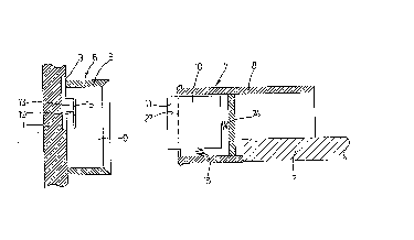
Fig. 4 and 5 show both connector parts of an
embodiment of the connector assembly according to the
invention for connecting for example an optical fibre
cable to optical fibres embedded in a printed circuit
board 25. In the same manner as in the printed circuit
board 1 the guiding plate 3 with guiding channels 4 for
the optical fibres is embedded in this printed circuit
board 25. In this case a housing 26 having a reverse
U-shape in cross-section is provided, said housing 26
bridging the guiding plate 3. A spring element 27 is
mounted in the housing 26 in an inner wall 28 extending
parallel to the guiding channels 4 of the guiding plate
3. A spring element 30 is provided in an upper wall 29.
Fig. 4a-c show a guiding plate 31, which is mainly
made in the same manner as the guiding plate 11. This
guiding plate 31 is provided with guiding channels 12 for
the optical fibres of the fibre cable not shown. The
slot 16 with the reference surface 17 is provided in the
guiding plate 11. The slot 21 of the guiding plate 31
joins in this case the slot 16. The-reference surface 22
of the slot 21 operates as a stop 5 surface co-operating
with the reference surface 20 of the projection 19 of the
guiding plate 3.
B
~ a ~
For realizing a connection between the optical
fibres of the the fibre cable and the optical fibres of
the printed circuit board 25 the guiding plate 31 is
inserted into the housing 26 from the left side according
to the view of fig. 5b, wherein the spring element 27
presses the reference surface 17 of the slot 16 against
the reference surface 14 of the projection 13. The
aligning edges 15 are provided in this case at the
longitudinal ends of the projection 13. The reference
surface 22 of the slot 21 meets with the reference
surface 20 of the projection 19. The spring element 30
presses together the contact pads of the conductors.
Although the guiding plate 31 is not mounted in a
housing in the embodiment of fig. 4 and 5, it is of
course also possible to mount the guiding plate 31 in a
suitable housing.
Therefore the invention is not restricted to the
embodiments as described above, which can be varied in a
number of ways within the scope of the claims.
R