Note: Descriptions are shown in the official language in which they were submitted.
2096393
PLASMA VAPOR DEPOSITION APPARATUS
FIELD OF THE INV~NTION
The present invention relates to a plasma vapor
deposition apparatus. More particularly, the present invention
relates to an inline plasma vapor deposition apparatus which
permits formation of a high-quality film at a high efficiency
and is useful for formation of a multilayer film.
PRIOR ART AND PROBL~MS
Along with the rapid development of technical
innovations in such areas as electronics and optoelectronics,
greater hopes are toward functional thin film materials, and
efforts are actively made for research and development for
forming a high-quality thin film and forming a multilayer film.
For the purpose of forming such a thin film various
means including vacuum vapor deposition, sputtering and plasma
vapor deposition are examined, and some of these means have
already been practically applied.
From among these methods, it is known that sputtering is
excellent in productivity, and high-frequency excitation,
particularly plasma vapor deposition based on plasma excitation
using coil-shaped electrodes is, on the other hand, excellent in
such properties as uniformity and adhering strength of the film.
Accordin~ to these conventional methods, however,
permitting formation of a film excellent in quality and
performance is not always compatible with achieving a higher
"~,
productivity. It has therefore been very difficult, for a
liquid crystal cell at a high productivity, or to form a
multilayer film continuously.
The sputtering method, for example, has been
defective in that it has been difficult to uniformly
distribute film-forming substances on a substrate or to
achieve a uniform chemical composition of a film, and
pinholes and deterioration have easily been caused. Higher
expectations have therefore been entertained on the plasma
vapor deposition as described above.
In the case of this plasma vapor deposition
method, however, it is necessary to take a greater care
than in sputtering as to the exciting means and vacuum
evacuation which cover the formation of the plasma space
and handling of the vapor source materials, and it has not
been easy to embody such a method as a continuous process
of a high productivity.
The present inventor has proposed, in Japanese
Patent Publication No. 21109/1980, published in 1980, for
example, a plasma vapor deposition apparatus having a
plurality of vapor deposition sections partitioned with
electromagnetic shielding plates, arranged in succession.
Even according to this apparatus, however, possibility has
been limited to permit formation of a high-quality film at
a high efficiency. It has been impossible also to cope
with formation of a multilayer film.
SUMMARY OF THE INVENTION
The present invention has therefore an object
to provide
~.~
~,~
2096593
~~ novel inline plasma vapor deposition apparatus which solves
the above-mentioned drawbacks in the conventional technologies,
permits formation of a high-quality high-performance film at a
high productivity and allows formation of a multilayer film
while utilizing the favorable merits of the plasma vapor
deposition method.
With a view to solving the above-mentioned problems, the
present invention provides a vacuum plasma vapor deposition
apparatus which comprises a vapor source supply means, a high-
frequency exciting means and a substrate holding means means
arranged above these means, wherein said vapor source supply
means has a drive and a circular holding plate connected thereto
and rotating horizontally, said circular holding plate being
provided with a rotation shaft and a concentric vapor source
material carrying section arranged on the surface thereof, and
said high-frequency exciting means is provided with coil-shaped
electrodes. The present invention provides also a vacuum inline
plasma vapor deposition apparatus which comprises an inlet and
an outlet of a substrate at the both ends of the apparatus line,
one or more vapor deposition sections permitting independent
evacuation to vacuum and evacuating sections before and after
same, arranged in series therewith, and a transport means,
provided in each of the vapor deposition sections and the
evacuating sections, allowing continuous passage, wherein said
apparatus has a vapor source material supply means in which at
least one vapor deposition section has a rotation shaft on a
circular holding plate connected to a drive and rotating
2096593
~rizontally and a mounting section of a vapor source material
on a concentric surface, and a high-frequency exciting means
provided with coil-shaped electrodes below the passing
substrate.
BRIEF DESCRIPTION OF THE DRAWINGS
Fig. 1 shows a plan view and a front view illustrating
an embodiment of the inline apparatus of the present invention;
Fig. 2 shows a perspective view illustrating the
embodiment of the inline apparatus of the present invention;
Fig. 3 shows a perspective view illustrating the
embodiment of the inline apparatus of the present invention;
Fig. 4 shows a sectional view illustrating an embodiment
of the high-frequency exciting vapor deposition section;
Fig. 5 shows a plan view illustrating an embodiment of
the film thickness correcting plate;
Fig. 6 shows a partial perspective view illustrating
another embodiment of the apparatus of the present invention;
Fig. 7 shows a plan view illustrating further another
embodiment of the inline apparatus of the present invention;
Fig. 8 shows a front view corresponding to Fig. 7:
Fig. 9 shows a partial perspective exterior view
corresponding to Figs. 7 and 8;
Fig. 10 shows a partially cutaway perspective view
corresponding to Fig. 9;
Fig. 11 shows a sectional view illustrating an
embodiment of the high-frequency exiting vapor deposition
section;
Fig. 12 shows a plan view illustrating an embodiment of
2096S93
~e film thickness correcting plate; and
Fig. 13 shows a plan view illustrating a further another
embodiment of the inline apparatus.
DETAILE~D DESCRIPTION OF THE INVENTION
The vacuum plasma vapor deposition apparatus of the
present invention will be described below with reference to the
attached drawings. The description below covers an inline
apparatus as a continuous production line.
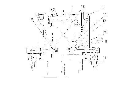
The attached Fig. 1 covers a plan view and a front view
illustrating an embodiment of the inline plasma vapor deposition
apparatus of the present invention, and Fig. 2 and 3 are
partially cutaway perspective views thereof. In the present
invention, as shown in Figs. 1, 2 and 3, the apparatus has an
inlet ~2~ and an outlet ~3) of a substrate ~1) at the both ends
of the apparatus line, one or more vapor deposition sections ~4)
and vacuum evacuating sections ~5a) and ~5b) before and after
the same, permitting independent vacuum evacuation. The inlet
~2) and the outlet ~3) of the substrate ~1) are provided with a
lift mechanism ~6) of the substrate ~1).
The apparatus has transport means ~7a)and ~7b) for
causing the substrate ~1) to continuously pass above the vapor
deposition section ~4) and the vacuum evacuating section ~5).
Fig. 3 illustrates an example of transportation of the substrate
~1). The transport means is provided with, for example, a
return mechanism.
The inline plasma vapor deposition apparatus of the
2096593
p~esent invention comprising the above-mentioned line
composition has a vapor source material supply means having a
vapor source material (9) mounted on a horizontally rotating
holding plate (8~ in a vacuum chamber as at least one vapor
deposition section (4~, and a high-frequency exciting means
provided with coil-shaped electrodes arranged below the passing
substrate (1).
The substrate (1~ is supported at the inlet (1) by a
moving section (~a) as a transport means, and is transported by
sliding along opposite rail sections ~7b). The substrate (1) is
transported through a vacuum-evacuated space in the vacuum
evacuating section (5a) forming the first-half step of the vapor
deposition section (4), and introduced into the vapor deposition
section (4) under the vacuum condition. In this vapor
deposition section (4), the substrate (1) is subjected to a
prescribed film forming treatment, and then transported to the
vacuum evacuating section (5b) forming the latter-half step of
the section. In this case, the substrate (1) may be
preliminarily heated at a prescribed point in the first-half
step of the vacuum evacuating section (5a). The vacuum
evacuating sections (5a) and (5b) form a buffer space, connect
the spaces between individual vessels appropriately with vacuum
gate valves fo as to allow each thereof to be independently
evacuated, including the vapor deposition sections (4).
The vapor deposition section (4) provided with a high-
frequency exciting means comprising coil-shaped electrodes is
provided, as shown in Figs, 1 and 2, for example, with a door
-- 6
2096~9~
~.0) capable of being opened and closed on the both sides of the
travelling direction of the substrate (1), and as shown in the
sectional view given in Fig. 4. a vapor source supply means,
arranged opposite thereto, having a vapor source material (g)
mounted on the above-mentioned holding plate ~8) horizontally
rotating at a point crossing at right angles the travelling
direction of the substrate (1) passing above the same. This
holding plate (8) rotates around a center axis (A) by the action
of a driving means (11), so that, for example, uniform
evaporation is permitted by the continuous rotation of the vapor
source material (9) mounted on an arcuate groove of the holding
plate (8). ~vaporation of this vapor source material (g) is
accomplished by an appropriate means such as resistance heating,
induction heating, electron beam (EB) or ion beam irradiation.
In the example shown in Fig. 4, an electron beam
irradiating means (12) is provided so that the vapor source
material (g) is evaporated under the effect of beam from this
electron beam irradiating means (12). ~vaporated particles of
the material are plasma-exclted by the high-frequency exciting
means comprising coil-shaped electrodes (14) while controlling
evaporation by means of a shutter (13), and form a film on the
substrate (1) with excited ions and radicals.
By continuously evaporating the vapor source material
(9) mounted on the horizontally rotating holding plate (8), and
oppositely arranging this vapor source supply means at right
angles to the travelling direction of the substrate (1), it is
possible to achieve uniform evaporation and uniform formation of
2096~93
~ film by plasma excitation of evaporated particles effected by
the coil-shaped electrodes, thus permitting achievement of
uniform properties including the film structure, film thickness
and adhering strength. The condition of the vapor source
material (9) can be observed through a quartz monitor ~15).
While the film is formed during the travel of the
substrate (1), the above-mentioned uniformity is sufficiently
ensured during this formation of the film during the travel.
With a view to further maintaining this uniformity, a film
thickness correcting plate ~16), is also provided on the
apparatus of the present invention. This correcting plate (16)
is to avoid duplication of the excited particles on the surface
of the substrate ~1~ to keep a satisfactory uniformity.
Usually, as shown in ~ig. 5, partial shielding is effected by
means of the correcting plate (16) in the travelling direction
(B) of the substrate ~1). The shape thereof should preferably
be variable according to the shape and arrangement of the vapor
source material supply means, the kind of the vapor source
material ~9), and the condition of film formation.
As to the substrate ~1), it is desirable to arrange a
heater ~17) so as to permit heating of the substrate ~1) from
back, as shown in Fig. 4.
With regard to the vapor deposition section ~4), an
impressing means of bias voltage to the substrate (1), and a
supply means of a reactive gas and an inert gas for forming a
plasma space should appropriately be arranged.
High-frequency excited plasma from the coil-shaped
i.~,
electrodes (14) can be generated according to various known
conditions: for example, a film can be formed through
plasma reaction by evaporation of any of such
solid substances and metals, alloys, inorganic matters
and polymers through vacuum evacuation to about 1 x 10⁻⁵
to 1 x 10⁻⁴ Torr and introduction of an inert gas such as
argon or helium, and furthermore, introduction of oxygen,
nitrogen, hydrogen, hydrocarbon or a polymerizable monomer.
For example, by using ITO (indium-tin oxide) as
the vapor source material, and introducing an inert gas and
oxygen gas, it is possible to generate a high-quality ITO
thin film at a high productivity on a glass substrate, for
example.
It is possible to form this film at a temperature
lower than that in the conventional method such as 200 to
300~C.
In the present invention, as shown in Fig. 6, for
example, it is possible to form a film of a different
material or multilayer film at a prescribed portion on the
masked substrate by arranging a plurality of vapor
deposition sections (4a) and (4b).
With the construction as described above, a color
filter substrate, for example, can be formed, after plasma
vapor deposition of a metal or an inorganic matter, by
plasma vapor deposition of an organic thin film, or
multilayer vapor of a pigment substance. Formation of such
a color filter can be accomplished continuously with
formation of an ITO film.
Ordinary vacuum vapor deposition or plasma,
a vapor deposition other than the coil-shaped electrode
method may be
2096~93
3~mbined with plasma vapor deposition.
Figs. 7 and 8 illustrate another embodiment of the
inline plasma vapor deposition apparatus of the present
invention.
As shown in the plan view of Fig. 7 and the front view
of Fig, 8, the apparatus of this embodiment has an inlet-outlet
section ~23) of the substrate ~21) in a region partitioned from
the line end of the apparatus, and pallet transport relay
elevator sections (24) and (25) arranged at the both ends of the
line. In the middle of the line, one or more vapor deposition
section(s) (26) permitting independent vacuum evacuation, and
vacuum evacuating sections (27a) and ~27b) before and after the
same are arranged. The apparatus is provided with a return
mechanism ~31), shown in Fig. g, for taking out the transport
pallet ~22) (charged with the substrate (21)) taken out from the
vacuum chamber and returning the pallet (22) to the outlet
section (23).
This apparatus has a transport means (30) for
continuously causing the substrate (21) to pass above the vapor
deposition section (26) and the vacuum evacuating sections (27a)
and (27b). Fig. 10 illustrate transportation of the substrate
(21). This transport mechanism (30) has the above-mentioned
return mechanism (31~ in the upper region thereof.
In the inline plasma vapor deposition apparatus having
the line construction as described above, a vapor source
material supply means mounting a vapor source material (33) on a
horizontally rotating holding plate (32) in the vacuum chamber,
-- 10 --
2096~9~
d a high-frequency excitation means provided with coil-shaped
electrodes (39) arranged below the travelling substrate ~21~.
The substrate (21) is charged on the transport pallet
~22) at the inlet-outlet section ~23), and sent to the relay
elevator ~24) by means of a transport mechanism ~29~. The
substrate ~21) is then transported to an inle~ chamber ~28a),
supported by the transport mechanism ~30) comprising a drive
rotation mechanism and and a belt drive sliding mechanism for
slide transportation. The substrate (21) is transported in a
vacuum-evacuated space in the vacuum evacuating section (27a)
forming the first-half step of the vapor deposition section
~26), and introduced into the vapor deposition section ~26)
under the vacuum condition. In this vapor deposition section
(26), the substrate (21) is subjected to a prescribed film
forming treatment, and transported to the latter-half step of
the vacuum evacuating section (27b). In this case, the
substrate (21) may be preliminarily heated or subjected to a
plasma treatment prior to film formation at a prescribed
position in the first-half step of the vacuum evacuating section
~27a). The vacuum evacuating sections (27a) and (27b) form a
buffer space so that individual vessels are appropriately
connected with vacuum gate valves in between and the vessels,
including the vapor deposition section (26), can be
independently vacuum-evacuated.
The substrate ~21) having a film formed thereon is taken
out from the outlet chamber ~28b) onto the pallet transport
relay elevator ~25) and returned by means of the return
-- 11 --
209G~9~
~echanism (31).
The vapor deposition section (26) provided with the high-
frequency exciting means comprising the coil-shaped electrodes
has, as shown in Figs. 7 and 8 for example, a door (36~ capable
of being opened and closed of the side of the travellin~
direction of the substrate (21), and i5 provided, as shown in
the sectional view given in Fig. 11, with a vapor source supply
means having the above-mentioned holding plates (32) rotating
horizontally, carrying the vapor source material ~33~ oppositely
arranged at a position substantially perpendicularly to the
travelling direction of the substrate (21) passing above the
same, with a replenishing mechanism (34~ of the vapor source
material (34). The holding plate (32) rotates around the center
axis A thereof by the action of a driving means (3~), so that
the vapor source material (33) carried in the arcuate groove of
the holding plate (32), for example, continuously rotates to
permit uniform evaporation thereof. The vapor source material
(33) can be continuously supplied by the replenishing mechanism
(34) to the holding plate (32), as shown in Fig. 11.
Evaporation of the vapor source material (33) may be
accomplished by an appropriate means such as resistance heating,
induction heating, electron beam (EB) or ion beam irradiation.
In the embodiment shown in Fig. 11, the apparatus is
provided with an electron beam irradiating means (35) so that
the vapor source material (~) can be evaporated under the effect
of the beam from this electron beam irradiating means (35). The
evaporated material particles are plasma-excited by means of the
- 12 -
2096~93
~gh-frequency exciting means comprising coil-shaped electrodes
(39) while controlling vapor by a shutter (38), and a film is
formed on the substrate ~21) with the thus excited ions and
radicals.
By causing continuous evaporation of the vapor source
material (33) carried on the horizontally rotating holding plate
~32), and by arranging the vapor source supply means opposite to
each other substantially perpendicularly to the travelling
direction of the substrate (21), it is possible to achieve
uniform formation of a film through plasma excitation of vapor
particles by evaporation and the coil-shaped electrodes, and
uniform properties such as the film structure, film thickness
and adhering strength. The state of the vapor source material
(33) can be observed by means of a ~uartz monitor or an EIES
monitor ~40) using exciting source based on electron
bombardment.
The film is formed during travel of the substrate ~21),
and the above-mentioned uniformity is maintained in film
formation during travel. With a view to further ensuring this
uniformity, a film thickness correcting plate (42) is provided
in the apparatus of the present invention. This correcting
plate ~42) is to ensure a uniform film thickness by avoiding
overlapping of the excited particles onto the surface of the
substrate (21~. In the case of this embodiment as shown in Fig.
12, the correcting plate ~42) acts as a partial shielding in the
travelling direction ~B) of the substrate ~21). It is needless
to mention that the shape thereof should preferably be variable
- 13 -
20g6~93
cr~l accordance with the shape and arrangement of the vapor source
material supply means, kind of the vapor source material (33),
and the condition of film formation.
It is desirable to provide a heater (41) so as to permit
heating of the substrate ~21) form behind, as shown in Fig. 11.
For the vapor deposition section (26), an impressing
means of bias voltage onto the substrate (21) and a supply means
of a reactive gas and an inert gas for producing a plasma space
are of course appropriately arranged.
High-fre~uency excited plasma may be produced from the
coil-shaped electrodes (39) under conventionally known
conditions as described above; under a vacuum condition of about
2 x 10 to 10 Torr, for example, a film can be formed by
plasma reaction caused by evaporation of a solid material such
as a metal, an alloy, an inorganic matter or a polymer through
introduction of an inert gas such as argon or helium from the
gas introducing mechanism (43) and introduction of oxygen,
nitrogen, hydrogen, and hydrocarbon or polymerizable monomer.
It is possible to form a high-~uality ITO (indium-tin
oxide) thin film on a glass substrate, for example, at a high
productivity by using ITO as the vapor source material and
introducing an inert gas or oxygen gas.
In this embodiment, furthermore, it is possible to form
a film of a different substance on a prescribed portion of a
masked substrate or a multilayer film by arranging, as shown in
Fig. 13, a plurality of vapor deposition sections (26a) and
(26b).
7~ 3
i ..
With the construction as described above, a color
filter substrate can for example be formed by plasma-vapor
depositing an organic thin film after plasma vapor
deposition of a metal or an inorganic matter, or a pigment
substrate into multiple layers. Formation of a color
filter can be continuously associated with formation of an
ITO film.
When forming an ITO film (1,5000 A) by means of
an apparatus having a single vapor deposition section as
shown in Figs. 7 to 12, the following configurational
specifications should be complied with:
~ Film : ITO (1,500 A)
~ Effective dimensions for attachment of substrate
840 mm wide x 930 mm long
~ Number of attached substrates
four 400 mm x 450 mm substrates/carrier
pallet
~ Film Thickness distribution: within i 5%
~ Heating of substrate: 250 to 300~C (350~C max.)
~ Throughput: minimum cycle time (two minutes)
~ Daily production: 120 pieces/hr x 24 hr/day
= 2,880 pieces/day
~ Electric power required for utility
3-phase, 200 V
about 220 kVA
50/60 Hz.
In the case of the apparatus having two vapor
deposition
2096~93
'~ctions ~26a)and (25b) as shown in Fig. 13, it is possible to
form an ITO multilayer film, or a multilayer film of SiO2 and
ITO.
It is needless to mention that various other details are
possible for the apparatus of the present invention.
As typically represented by the above embodiments of the
present invention, the followin~ excellent effects are
available:
1) By adopting the high-frequency plasma vapor
deposition process and permitting continuous supply
of the vapor source material, it is possible to form
a high-quality film with uniform properties such as
structure, film thickness and adhering strength at a
lower temperature.
2) As film formation proceeds while the substrate
passes continuously above the vapor source material,
a very large throughput is available.
3) Continuous film formation of various film materials
is possible.
4) It is easier to form a multilayer film by installing
a plurality of vapor deposition sections.
5) Continuous supply of the vapor source material
permits stable and continuous formation of a film.
6) By providing a return mechanism as a transport
means, it suffices to install an inlet-outlet
section in the clean room.
- 16 -