Note: Descriptions are shown in the official language in which they were submitted.
2097118
,
LIOUID L~v~L CONTROL WITH CAPA~ v~ SENSORS
The present invention relates to control
circuits for pump motors. More specifically, the
field of the invention is that of liquid level
control circuits which automatically maintain the
liquid level within a predetermined range.
In sump and water tanks, for example, the
liquid level should be maintained within a
predetermined range for proper functioning of the
tank. Many prior art devices automatically
control the liquid level within the tank by
- activating a pump when the liquid rises above a
first predetermined level and deactivating the
pump when the liquid level falls below a second
predetermined level. Some of the prior art
devices use mechAnical or moving parts such as
mechanical switches operated by rubber diaphragms,
springs, rods, floats, or balls, all of which may
tend to wear out or malfunction over time.
Other prior art devices use electrical or
optical probes positioned within the tank to
determine the liquid level and control the pump
accordingly. For example, self-heating
thermistors or conductivity probes may be used.
However, such Prior art systems using probes may
be sensitive to humidity, moisture, changing
temperatures, and varying voltage levels in the
sensing circuit, all of which may produce
erroneous results and subject the probes to wear.
Also, contamination of the probes may adversely
effect their performance. The probes and their
associated circuitry may be adjusted to improve
performance, but making the adjustments may be
inconvenient and expensive.
- 35 Employing capacitive sensors for liquid level
control provides advantages including the
'~'
- 2~97118
prevention of triggering from transient water
imbalances, such as splashes or waves, by
precisely defining the required charging time of
the capacitive sensors. However, the charging
time may vary over operating temperatures in each
unit, and similar units may vary in charging time
because of variations in the electrical components
of the control. Such variations may cause some
controls to be activated falsely. In order to
prevent any such occurrences, a desired feature of
a liquid level control is to minimize variations
in charging time, and therefore the time needed
for actuation.
The charging time required for capacitive
sensors is at least in part determined by the size
of the resistors in the charging circuit. For
applications which charge the capacitive sensors
solely on the basis of the alternating current
cycle (60 Hz), the resistances required are large
in order to keep the capacitive sensors from
completely charging every cycle. However, one
problem with large resistances is that they are
susceptible to receipt of radio frequency (RF)
energy due to the antenna effect. The antenna
effect or strays from the AC source may cause
unexpected charging of capacitive sensors.
What is needed is a liquid level control
which minimizes variations in actuation time.
Another need is for a liquid level control
which reliably operates without the need for
adjustment.
Also needed is a liquid level control which
minimizes operating problems associated with
contamination and mechanical wear.
3S A further need exists for a liquid level
control which minimizes inaccuracies associated
2097118
with varying temperatures and high resistances.
The present invention is a liquid level
control system utilizing capacitive sensors which
avoids the aforementioned problems. Activating
circuitry starts the pump motor when both upper
and lower sensors indicate the presence of liquid.
The activating circuitry includes a high frequency
oscillator circuit which determines the charging
time of the capacitive sensors. The pump motor
continues operation until the lower capacitive
sensor indicates the absence of liquid, in which
case the pump is shut off. A heatsink in the
control circuitry provides a means for cooling a
power semiconductor switch. The circuitry of the
present invention operates reliably over a wide
range of operating conditions.
One construction of a capacitive sensor
includes having one electrode as a metal plate
disposed in a plastic box enclosing the circuitry,
and the other electrode as the pump case. This
provides a simple and reliable capacitive sensor
which is free of any problems of me~nical
failure. Alternatively, a capacitive sensor may
include an insulated wire capable of mounting at
any position in the tank.
One electrode of the capacitive sensor
disposed in the plastic box may be a suitably
sized flat, U-shaped, or cup shaped metal plate.
The plate acts as a heatsink for the liquid level
control, particularly for the power switch, so
that performance variations due to temperature are
minimized. The plate is disposed on the bottom of
the plastic box, in contact with the surface of
the box which is generally in thermal contact with
the water. Thus, the metal plate performs two
- functions, one as an electrode for the sensor and
-- 2097118
the other as a heat dissipating device.
One portion of the circuitry includes
thermistors which can turn off the pump motor when
a predetermined temperature is reached. This is
particularly important when the system is operated
in a circulating mode wherein the liquid pumped
out of the tank is returned to the tank and the
water temperature would otherwise become
increasingly higher.
Another portion of the circuitry maintains
switch terminal voltages within predetermined
levels so that false triggering of the activating
circuitry does not occur, which can be
particularly troublesome at high operating
temperatures. Also, another portion guards
against damage to the power switch by ensuring
voltages stay within rated limits.
Another aspect of the invention involves a
high frequency oscillator which precisely
maintains charging times for the capacitive
sensors. The high frequency oscillator minimizes
the resistances required to operate with the
capacitive sensors. The lower resistances are
less susceptible to influence by RF signals or AC
power source variations.
The present invention is, in one form, an
apparatus for controlling liquid levels comprising
a pump, a motor drivingly connected to the pump,
two sensors, an activating unit, and a heatsink.
The first sensor detects the presence of liquid
and is mounted at a first vertical position; it
includes a capacitive circuit having two
capacitive electrodes which produces a first
signal indicative of the presence of liquid at the
first position. The second sensor detects the
presence of liquid and is mounted at a second,
- 2097118
-
different vertical position; it includes a
capacitive circuit having two capacitive
electrodes which produce a second signal
indicative of the presence of liquid at the second
position. The activating unit enables the motor
and is operably coupled to the sensors; it starts
the motor to drive the pump when both of the
sensor signals are produced, continues operation
of the motor while at least one of the sensor
signals are produced, and stops the motor when
both sensor signals are no longer produced. The
heatsink transfers heat generated by the
activating unit to the surrounding liquid whereby
the temperature of the activating unit is
maintained within rating limits of its components
so that variations in the response time of the
activating unit are minimized.
The above mentioned and other features and
objects of this invention, and the manner of
attaining them, will become more apparent and the
invention itself will be better understood by
reference to the following description of
embodiments of the invention taken in conjunction
with the accompanying drawings, wherein:
Figure 1 is a side, elevational view, in
partial cut-away, of the liquid control system of
the present invention.
Figure 2 is an enlarged cross-sectional view
taken along view lines 2-2 of Figure 1.
Figure 3 is a schematic circuit diagram of
the control circuitry of the present invention.
Figure 4 is a side, elevational view, in
partial cut-away, of an alternative embodiment of
the liquid control system of the present
invention.
Figure 5 is a schematic circuit diagram of
2G97118
the control circuitry of the embodiment of Figure
4.
Corresponding reference characters indicate
corresponding parts throughout the several views.
The exemplifications set out herein illustrates
preferred embodiments of the invention, in several
forms, and such exemplifications are not to be
construed as limiting the scope of the invention
in any manner.
The present invention comprises a liquid
level control system adapted for use in a tank or
other vessel in which the level of liquid is to be
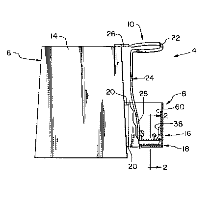
controlled. As depicted in Figure 1, control
system 4 includes pump 6, which can be a
submersible sump pump, controller box 8, and upper
sensor 10. The water in which control system 4 is
immersed acts as a conductive medium. Pump 6 is
disposed within the tank (not shown) in which the
liquid level is to be controlled, and includes
insulated motor 12 (see Figure 3) located within
pump casing 14. Controller box 8 is also disposed
within the tank, and is preferably attached to
casing 14. Circuit board assembly 16 and lower
sensor 18 are disposed within box 8. 80x 8 is
spaced away from pump casing 14 by mounting posts
20, and preferably box 8 is made of a dielectric
material. Upper sensor 10 includes sensor portion
22 of insulated wire 24 which is vertically
adjustable at an upper portion of pump casing 14
by means of mounting bracket 26. Sensor portion
22 is electrically coupled to circuit board 16 via
connecting portion 28 of insulated wire 24.
Figure 2 shows the arrangement of lower
sensor 18. Metal plate 30 is located on bottom
wall 32 of box 8 and is separated from any liquid
adjacent bottom wall 32 by the dielectric barrier
2097118
formed by the material of box 8, which is
preferably plastic or the like. Printed circuit
board assembly 16 is secured vertically above
plate 30 and is connected to metal plate 30 by
electrical wire 34. Epoxy potting compound exists
between circuit board assembly 16 and metal plate
30 so that assembly 16 and plate 30 are
electrically isolated.
Figure 3 shows the circuitry of the present
invention, most of which is generally located on
circuit board assembly 16. Alternating current
(AC) power supply 36 is selectively electrically
coupled to pump motor 12 by triac 38. Direct
current (DC) power supply 40 converts alternating
current from AC power supply 36 to a direct
current bus between DC positive terminal 44 and DC
negative terminal 42. Activating circuitry,
referred to generally by numeral 46, is connected
to the direct current bus and selectively
activates triac 38 according to the states of
upper and lower capacitive sensors C2 and C3 as
described in more detail below. Grounding wire 48
is connected to pump case 14 to provide a ground
for the AC circuit through pump motor 12. A more
detailed description of the circuitry of the
present invention is provided below by describing
the arrangement and operation of activating
circuitry 46.
Also shown in Figure 3, activating circuitry
46 includes astable multivibrator 50 and
monostable multivibrators 52 and 54. Astable
multivibrator 50 includes NAND gate G1, resistor
R1, and capacitor C1. NAND gate G1 has input pin
1 coupled to DC positive terminal 44, input pin 2
coupled to one terminal of resistor R1 and one
terminal of capacitor C1, and output pin 3 coupled
2097118
.
to the cathode of diode D3, the cathode of diode
D5, and the other terminal of resistor R1. The
other terminal of capacitor C1 is coupled to DC
negative terminal 44. The coaction of Rl and C1
causes output pin 3 of NAND gate G1' to change
state at a much higher frequency than the
frequency of line voltage from AC power supply 36.
Monostable multivibrator 52 includes NAND
gate G4, resistor R2, and upper sensor capacitor
C2. NAND gate G4 has input pin 12 coupled to DC
positive terminal 44 and one terminal of resistor
R2, input pin 13 coupled to the other terminal of
resistor R2, the anode of diode D3, and the series
circuit of capacitors C2 and C4, and output pin 11
coupled to the base of transistor Q2. The series
circuit of capacitors C2 and C4 includes one
terminal of capacitor C4 coupled to input pin 13
of NAND gate G4, the other terminal of capacitor
C4 coupled to one terminal of capacitor C2, and
the other terminal of capacitor C2 coupled to DC
negative terminal 42.
Monostable multivibrator 54 includes NAND
gate G2, resistor R3, and lower sensor capacitor
C3. NAND gate G2 has input pin 6 coupled to DC
positive terminal 44 and one terminal of resistor
R3, input pin 5 coupled to the other terminal of
resistor R3, the anode of diode D5, and the series
circuit of capacitors C3 and CS, and output pin 4
coupled to the cathode of diode D4. The series
circuit of capacitors C3 and C5 includes one
terminal of capacitor CS coupled to input pin S of
NAND gate G2, the other terminal of capacitor C5
coupled to one terminal of capacitor C3, and the
other terminal of capacitor C3 coupled to DC
negative terminal 42.
Capacitors C4 and C5 are not needed to
2097118
achieve the desired functionality of monostable
multivibrators 52 and 54. As a precautionary
measure, however, capacitors C4 and C5 are
included in activating circuitry 46 to limit the
amount of current which could potentially pass
through the liquid in case that insulation on the
plastic case adjacent the sensor plates or on any
of the sensor wires is damaged.
NAND gate G3 is coupled to monostable
multivibrator 54 via diode D4, wherein the anode
of diode D4 is coupled to input pin 8 of NAND gate
G3. Resistor R8 is also coupled between DC
positive terminal 44 and input pin 8, and
capacitor C8 is coupled between input pin 8 and DC
negative terminal 42. Input pin 9 of NAND gate G3
is coupled to voltage divider 56, which includes
resistor R9 coupled between DC positive terminal
44 and input pin 9, and negative temperature
coefficient (NTC) thermistor R4 coupled between
input pin 9 and DC negative terminal 42. Output
pin 10 of NAND gate G3 is coupled to the base of
transistor Q1.
Transistor Q1 is disposed in negative gate
current path circuit 58 to switch the gate current
of triac 38. Triac 38 conducts AC line current
when current flows through negative gate current
path circuit 58. Current path circuit 58 includes
the gate of triac 38 which is coupled to one
terminal of resistor R7, the other terminal of
resistor R7 which is then coupled with the anode
of SCRl, the cathode of SCR1 which is then coupled
to the emitter of transistor Q1, and the collector
of transistor Q1 which is finally coupled to DC
negative terminal 42. Further, resistor R11 has
one terminal coupled to DC positive terminal 44
and the other terminal coupled to the cathode of
- 2~97118
SCR1 and the emitter of transistor Q1 for
maintaining the emitter of transistor Ql at
several tenths of a volt above DC negative
terminal 42 when Q1 is in a con~l~ctive state.
SCR1 also switches current path circuit 58 by
means of capacitor C9, resistor R6, and transistor
Q2. Capacitor C9 has one terminal coupled to DC
negative terminal 42 and the other terminal
coupled to the gate of SCR1, one terminal of
resistor R6, and the emitter of transistor Q2.
This arrangement allows capacitor C9 to charge
from DC positive terminal 44 through resistor R6,
and discharge when the base of transistor Q2 is
conducting to the output terminal of NAND gate G4,
through the collector of transistor Q2 which is
coupled to DC negative terminal 42. When the base
of transistor Q2 is not conducting, voltage on
capacitor C9 rises to a voltage sufficient to
trigger the gate of SCR1, thus closing current
path circuit 58 from the gate of triac 38 to the
emitter of transistor Q1.
DC power supply 40 includes capacitor C11,
Zener diode D1, diode D2, capacitor C7, and
resistor R5. DC positive terminal 44 is the same
as the AC line labeled HOT, and DC negative
terminal 42 is the negative terminal of
electrolytic capacitor Cll. Capacitor C11 is
coupled between DC positive terminal 44 and DC
negative terminal 42. The cathode of Zener diode
Dl is coupled to DC positive terminal 44 and the
anode of Zener diode Dl is coupled to the cathode
of diode D2 and one terminal of capacitor C7. The
anode of diode D2 is coupled to DC negative
terminal 42, while the other terminal of capacitor
C7 is coupled to one terminal of resistor R5. The
other terminal of resistor R5 is coupled to the
2097118
common return line (labeled COMMON) of AC power
supply 36.
In accordance with the present invention,
upper and lower sensors 10 and 18, respectively,
comprise capacitive s~Cors C2 and C3,
respectively. Upper capacitive sensor C2 includes
the insulation on sensor portion 22 of insulated
wire 24 which forms the electrode of capacitor C2,
and the other electrode of capacitor C2 may
include lead wires or other conductors having
insulation, or alternatively pump casing 14 (with
the insulated motor and circuit lead wires).
Lower capacitive sensor C3 has metal plate 30 as
one electrode and pump casing 14 (with the
insulated motor and circuit lead wires immersed in
water) as the other electrode. Alternatively,
lower capacitive eD~Cor C3 may have an insulated
wire (similar to s~nsor portion 22 of upper sensor
10) as one electrode and pump casing 14 (with the
insulated motor and circuit lead wires) as the
other electrode. With the structure of upper and
lower capacitive s~ors C2 and C3, the sensing
circuitry is much less vulnerable to physical
contamination or physical wear.
In operation, the liquid level rises from an
empty state due to external conditions, but pump 6
does not operate until after upper sensor 10 is
submerged in liquid. When lower sensor 18 is
covered by liquid, the capacitance of capacitive
sensor C3 is sufficiently large that the voltage
at input pin 5 of gate G2 does not exceed the trip
threshold so that output pin 4 of gate G2 stays
high. Diode D4 does not allow capacitor C8 to
discharge, and resistor R8 is able to charge
capacitor C8 above the trip voltage of gate G3 at
input pin 8, causing output pin 10 of gate G3 to
- 2097118
drop to a low voltage which is only slightly above
negative DC terminal 42. Pin 10 of gate G3 can
then receive current from the base terminal of
transistor Ql and activating circuitry 46 is then
in an enabled state.
As the water level rises and reaches upper
sensor 10, the capacitance of capacitive sensor C2
increases to a value such that the voltage at pin
13 of gate G4 does not exceed the trip threshold
voltage. Consequently, pin 11 of gate G4 stays at
a high voltage preventing transistor Q2 from
conducting. Capacitor C9 charges through resistor
R6, and as the voltage on C9 rises slightly above
1 volt, the gate of SCRl receives a triggering
current. Therefore, SCRl conducts current which
passes through a path including main terminal 1
(MT1) and the gate of triac 38, resistor R7, the
anode-cathode of SCRl, and the emitter-collector
of transistor Q1. Current path circuit 58 and
resulting negative triac gate current causes triac
38 to conduct AC current through motor 12.
In operation, the liquid level drops from a
full state wherein both capacitive sensors C2 and
C3 are immersed and motor 12 is actively driving
pump 6. Eventually, an electrode of the upper
capacitive sensor C2 is uncovered, and pin 11 of
gate G4 is tripped low toward the end of the AC
cycle of astable multivibrator 50. Transistor Q2
conducts, periodically discharging capacitor C9.
Resistor Rll causes transistor Ql to have an
emitter voltage about several tenths above that of
DC negative terminal 42. The time constant of the
circuit comprising resistor R6 and capacitor C9 is
very large in comparison with ~isch~rge events
occurring through transistor Q2 so that voltage on
capacitor C9 is kept in a low state, removing the
- 2097118
gate current source for SCR1. However, due to the
SCR's latching characteristics, SCR1 remains in
conduction without need for gate current and
therefore triac 38 continues to supply current to
the pump motor. Further, the gate voltage of SCR1
is the difference between the emitter voltage of
transistor Q2 and the emitter voltage of
transistor Q1. This voltage difference is a very
low value when no gating current is desired.
Since this gives the effect of a shorted
gate-cathode, SCR1 may operate at high
temperatures while eliminating the occurrence of
false triggering.
After the water level has been pumped low
enough to partially uncover an electrode of lower
capacitive sensor C3, pin 4 of gate G2 drops to a
low voltage near the end of the astable
multivibrator cycle. With pin 4 of gate G2 low,
capacitor C8 discharges thus causing the ouL~
pin 10 of gate G3 to go high. This turns off
transistor Q1, thereby turning off SCR1 by
decreasing its anode current to a value below its
holding current. Without a triac gate current
through SCR1, triac 38 drops out of conduction at
the next zero crossing of the main terminals'
current.
Resistor R9 and NTC thermistor R4 form
voltage divider circuit 56 with input to pin 9 of
gate G3. Thermistor R4 is placed in thermal
contact with the case (not shown) of triac 38. If
triac 38 exceeds a predetermined temperature and
becomes overheated, thermistor R4 drops in
resistance and lowers the voltage at pin 9 of gate
G3 below the tip-off voltage, causing pin 10 of
gate G3 to go high and thereby turning off Q1.
Alternatively, R9 may be a positive temperature
2097118
coefficient (PTC) thermistor in thermal contact
with triac 38, and resistor R4 would then have a
fixed resistance.
Triac 38 is attached to heat spreader 60 and
is cooled by the liquid which surrounds the
control box 8 and pump 6. Pump 6 may operate in a
circulating mode whereby the liquid discharge of
pump 6 is L e ~ ,ed to the tank. In the
circulating mode, the liquid temperature
continually rises and may result in failure of
motor 12 or activating circuitry 46 unless the
heating process is interrupted. Thus, the
thermistor in conjunction with input pin 9 of gate
G3 forms both a motor protector and a circuit
protector.
The values of the circuit elements shown in
Figure 3 are given below in Table 1:
Element Value
Rl 220Kn
R2 100Kn
R3 100Kn
R4NTC Thermistor (Keystone)
RL1006-135.2K-138-Dl
R5 47n
R6 33Kn
R7 220n
R8 100KSI
R9 18Kn
R10 220n
Rll 18Kn
Cl 150pf
C2 50pf (UPPER SENSOR)
C3 50pf (LOWER SENSOR)
C4 0.0047~f, 200v
- 2097118
C5 0.0047~f, 200v
C7 2.0~f,200v
C8 2.2~f,16v
C9 2.2~f,16v
C10 O.l~f,200v
C11 470 ~f,16v
Ql,Q2 2N4126
SCR1 C103
TRIAC8 Amp, 400v, Iso Tab; (Teccor)
Q4008L4
Gl,G2,G3,G4 Quad 2-Input NAND Schmitt
Trigger CD4093BE
Dl 12v, lw Zener IN4742
D2 IN4001
D3 IN4001
D4 IN4001
D5 IN4001
~ABLE 1
The attributes of NTC thermistor R4 include a
resistance of 250 Kn at 25C with a resistance
ratio of 12 in the range of 0C to 50C. If the
alternative embodiment having R9 as a PTC
thermistor is used, R9 would preferably have
attributes including a resistance of 50n at 25C
with a transition temperature of 70C (for
example, using a Keystone RL3006-50-70-25-PTO),
and R4 would have a fixed resistance of 18Kn.
Figures 4 and 5 show an alternative
emhoA;ment of the present invention. The physical
209711~
variations shown in Figure 4 relate to the
heatsink arrangement and sensor mounting
arrangement of the liquid level control. This
provides greater heat dissipation for the CGll~ ol
circuitry, and the ability to change the location
of the sensors and thereby adjust minimum and
maximum water levels. The electrical circuit
variations shown in Figure 5 relate to the high
frequency astable multivibrator and the latching
circuitry. The activating circuitry of this
alternative embodiment provides im~Loved
performance in terms of minimizing charging time
variations by virtue of the higher frequency
astable multivibrator, while the modified latching
circuitry is less susceptible to variations due to
temperature changes.
As depicted in Figure 4, control system 62
includes pump 64, which can be a s~bmersible sump
pump, controller box 66, mounting tube 68, and
upper sensor 70. The water in which control
system 62 is immersed acts as a conductive medium.
Pump 64 is ~ispoc~ within the tank (not shown) in
which the liquid level is to be COll~ olled, and
includes in~ ted motor 72 (see Figure 5) located
within pump casing 74. Controller box 66 is also
disposed within the tank, and is preferably
attached to casing 74 as described in more detail
below. Circuit board assembly 76 and lower sensor
78 are disposed within box 66. Box 66 is spaced
away from pump casing 74 by the attachment of
bracket 80 to mounting posts 82, and preferably
box 66 is made of a dielectric material such as
plastic. Upper s~Cor 80 includes cover 84 having
conductive element 86 which may be ad~ustably
positioned vertically on mounting tube 68.
According to the present invention, lower
209711~
sensor 78 comprises netal plate 88 which is in
thermal contact with the power switching element
of circuit board assembly 76, which in the
embodiment of Figure S is TRIAC'. Metal plate 88
may be a flat plate of sufficient area and
thickness, or may have a U-shaped cross-section as
depicted in Figure 4 with the entire plate 86
having either a U-shaped or cup shaped structure.
Metal plate 88 is located against the bottom wall
of box 66, which is in thermal contact with
cooling liguid at almost every point of time
during operation of control system 62. For
example, a sufficient amount of metal would be
about 40 square centimeters (cm) of metal plate
lS having a thickness of about 0.18 cm, preferably
1100 grade aluminum. However, since metal plate
88 also functions as one of the electrodes of
lower sensor 78, TRIAC' must be an isolated triac
or else an insulating washer (not shown) must be
used to provide the needed electrical isolation.
According to another aspect of the present
invention, the minimum and maximum water levels
may be adjusted by means of bracket 80 and
mounting tube 68, respectively. Bracket 80 spaces
box 66 and plate 88 from pump casing 74 thereby
electrically isolating the two, wherein pump
casing 74 may be the other electrode for lower
sensor 78; bracket 80 further includes a plurality
of slots (not shown) located at various vertical
positions for engaging mounting posts 82 which
allows box 66 to be mounted at a plurality of
vertical positions. Upper sensor 70 is slidably
movable on tube 68 from the top of box 66 to an
upper position adjacent to mounting tube guide 90
which is attached at the top of pump casing 74.
Upper sensor 70 is held in a specific position by
2097I18
18
its interference fit around tube 68, although set
screws or other attachments may also be used to
fixedly position upper sensor 70.
Figure 5 shows the circuitry of the
alternative embodiment of the present invention,
most of the circuitry being generally located on
circuit board assembly 76. Alternating current
(AC) power supply 92 is selectively electrically
coupled to pump motor 72 by TRIAC' 94. Direct
current (DC) power supply 96 convérts alternating
current from power supply 92 to a direct current
bus between DC positive terminal 98 and DC
negative terminal 100. Activating circuitry,
referred to generally by numeral 102, is connected
to the direct current bus and selectively
activates triac 94 according to the states of
upper and lower capacitive sensors C10' and C4' as
described in more detail below. GL O~ g wire
104 is connected to pump case 74 to provide a
ground for the AC circuit through pump motor 72.
Activating circuitry 102 includes astable
multivibrator 106, monostable multivibrators 108
and 110, and lat~hing circuit 112.
In accordance with the present invention,
astable multivibrator 106 includes NAND gate G1',
capacitor C2' coupled to input pin 2 of gate G1',
resistor R2' coupled between input pin 2 and
output pin 3 of NAND gate G1', and a high
frequency oscillating circuit which includes
transistor Q2', resistor R3', and capacitor C3'.
The high frequency oscillating circuit is formed
by C3' having one terminal coupled to o~L~uL pin 3
of Gl' and the other terminal coupled to one
terminal of R3' and negative DC bus 100. The
other terminal of R3' is coupled to the base of
transistor Q2'. Q2' has its collector coupled to
- 2097118
19
input pin 2 of G1' and the one terminal of C2',
and its emitter coupled to negative DC bus 100 so
that conduction of Q2' allows for C2' to
discharge. The oscillating cycle of o~L~ pin 3
of NAND gate Gl' determines the charging time of
upper sensor C10' and lower sensor C4'.
When o~L~u~ pin 3 is high, diodes D2' and D3'
are biased off and are non-conducting, allowing
upper capacitor C10' to charge through resistor
R12' and lower capacitor C4' to charge through
resistor RS'. When o~L~ pin 3 is low, then
diodes D2' and D3' are forward biased and no
charging current reaches capacitive sensors C4'
and C10'. This causes periodic conduction of Q2'
and contributes to the reliability of the high
frequency cycling of astable multivibrator 106
which is at a predetermined time period because of
the high accuracy of the upper threshold of Gl'.
The accuracy of Gl', which is preferably a Schmitt
trigger device, is relatively constant from device
to device and over various operating conditions
so that tempe~a~u~e variations and manufacturing
variations have only a minimal effect on the
charging time. The high frequency of astable
2S multivibrator 106 (preferably about 100 kiloHertz)
allows for relatively small resistances to be
employed.
Latching circuit 112 operates to maintain
activation of activating circuitry 102 after the
initial triggering condition (liquid contact with
upper sensor 70) no longer exists by holding
transistor Ql' in a conductive state after upper
sensor 70 no longer contacts the liquid. Rather
than requiring a latching current, the conduction
3S of Ql' d~p~n~c on the state of pin 10 of gate G3'.
NAND gate G3' has its output pin 10 indirectly
2097118
coupled to the base of transistor Q1' through
resistor R10', and indirectly coupled to the gate
of TRIAC' through resistor R6'. NAND gate G3'
also has its input pin 8 coupled to capacitor C8'
(which is in turn coupled to negative DC bus 100)
and a voltage divider (which operates similarly to
divider circuit 56 of Figure 3) consisting of
resistor R8' (also coupled to positive DC bus 98)
and thermistor R4' (also coupled to negative DC
bus 100); and gate G3' has its input pin 9 coupled
to capacitor C9' and resistor R9'. The emitter of
Q1' is coupled to positive DC bus 98, while the
collector is coupled to input pin 9 of gate G3' as
well as to R9', the anode of D1', and C9'.
Monostable vibrators 108 and 110 have a
similar arrangement to monostable vibrators 52 and
54 of Figure 3, including the precautionary
arrangement of capacitors C12' and C5' to limit
current in the event of a short through the
controller case to the a~L~ounding liquid.
Monostable vibrator 108 is coupled to latching
circuit 112 at o~ L pin 11 to R9' and to the
collector of Q1' through resistor R11' and the
anode of diode D1'. Astable multivibrator 106 is
coupled to monostable vibrator 108 such that
output pin 3 of gate Gl' is coupled to input pin
12 of gate G4' through the anode of diode D2'; and
the oscillator circuit is coupled to monostable
vibrator 110 such that output pin 3 of gate G1' is
coupled to input pin 5 of gate G2' through the
anode of diode D3'. Monostable vibrator 110 is
coupled to latr~; ng circuit 112 at output pin 4 of
gate G2' to input pin 8 of gate G3' through the
anode of diode D4'.
In operation, the liquid level rises from an
empty state due to external conditions, but pump
2097118
64 does not operate until after upper sensor 70
contacts, or is submerged, in liquid. When lower
sensor 78 is covered by liquid, the capacitance of
capacitive s~ns~r C4' is sufficiently large such
S that the voltage at input pin 5 of NAND gate G2'
does not exceed its threshold so that gate G2'
does not trip and ou~ pin 4 stays high.
Transistor Ql' and NAND gate G4' do not allow
capacitor C9' to charge and raise input pin 9 of
NAND gate G3' above its threshold, so output pin
10 remains at a high potential and keeps TRIAC' 94
non-conductive.
As the liquid level rises and reaches upper
sensor 70, the capacitance of C10' increases and
capacitor C10', charging through R12', reaches
voltage peaks which are insufficient to trigger
NAND gate G4' and o~L~uL pin 11 goes high. This
allows capacitor C9' to charge through resistor
R9' which causes input pin 9 of NAND gate G3' to
go high and therefore output pin 10 goes low. The
low value of ~L~L pin 10 of G3' causes an
activating current through TRIAC' 94, thus turning
on pump motor 72. Also, transistor Ql' becomes
conductive in a latrhing loop so that C9' is
charged nearly to the positive DC bus by Q1'.
Hence, input pin 9 of NAND gate G3' stays high
even if ouL~ pin 11 of gate G4' goes low.
After activation of pump motor 72, the liquid
level drops by virtue of the pumping and
eventually an electrode of upper sensor 70 is
removed from contact with the liquid. However,
latching circuit 112 maintains activation of
TRIAC' 94 and provision of current to pump motor
72 provided that lower sensor 78 remains in
contact with the liquid. After the liquid has
been pumped sufficiently to lower the liquid level
209711~
below one of the electrodes of lower sensor 78,
output pin 4 of NAND gate G2' goes low and allows
C8' to discharge, breaking the latching loop by
virtue of one of the NAND inputs having dropped
too a low state. As a result, output pin 10 of
NAND gate G3' goes high and terminates the
activating current through the gate of TRIAC' 94
so that at the next zero-crossing of the
alternating current, TRIAC' 94 becomes
non-conductive.
Resistor R8' and NTC thermistor R4' form a
voltage divider circuit coupled with input pin 8
of gate G3'. Thermistor R4' is placed in thermal
contact with TRIAC' 94. If TRIAC' 94 exceeds a
predetermined temperature and becomes overheated,
thermistor R4' drops in resistance and lowers the
voltage at input pin 8 of gate G3' below the
trigger voltage, causing output pin 10 of gate G3'
to go high and thereby turning off TRIAC' 94.
Alternatively, R8' may be a positive temperature
coefficient (PTC) thermistor in thermal contact
with TRIAC' 94, and resistor R4' would then be
have a fixed resistance.
AC power supply 92 may be a conventional 115
VAC power source, and DC power supply 96 includes
Zener diode D6', diode D5', capacitor C1', and
resistor Rl' which are arranged similarly to the
arrangement of DC power supply 40 of Figure 3. In
addition to AC power supply 92 and DC power supply
96 coacting to provide a DC bus to activating
circuitry 102, protection device (metal oxide
varistor, or MOV1) 114 may be connected across the
AC mains to guard against voltage spikes from AC
power supply 92.
The values of the circuit elements shown in
Figure 5 are given below in Table 2:
- 2097118
~'
23
ement Value
Rl' 22 n
R2' 33 Kn
R3' 4.7 Kn
R4' NTC Thermistor (Panasonic)
ERT-D2FIL154S
R5' 100Kn
R6' 820 ~
R7' 820 n
R8' 20 Kn
R9' 220Kn
R10' 150KQ
Rll' 10 Kn
R12' 150Kn
Cl' 0.68 ~f, 250v
C2' 150pf
C3' 22pf
C4' 50pf (LOWER SENSOR)
C5' 4,700pf, 500v
C6' 470 ~f, 16v
C7' 0.1 ~f, 250v
C8-' 0.68 ~f, 35v
C9' 0.68 ~f, 35v
C10' 50Pf (UPPER SENSOR)
C12' 4,700pf, 500v
Ql',Q2' MPS 4126
TRIAC' 8 Amp, 400v, Iso Tab; (Teccor)
Q4008L4
Gl'-G4' Quad 2-Input NAND Schmitt
Trigger CD4093BE
Dl'-D4' IN4148 or lN914
2097118
24
DS' IN4001
D6' 12v, lw Zener IN4742
MOV1 Siemens S07X230 or Panasonic
ERZCO7DK36lU
TARr~ 2
The attributes of NTC thermistor R4' include
a resistance of 250 Rn at 25C with a resistance
ratio of 12 in the range of 0C to 50C. If the
alternative embodiment having R8' as a PTC
thermistor is used, R8' would preferably have
attributes including a resistance of 50n at 25C
with a transition temperature of 70C (for
example, using a Reystone RL3006-50-70-25-PTO),
and R4' would have a fixed resistance of 18Rn.
It should be understood that the signals
generated by the capacitive sensing circuits that
activate and deactivate the pump control circuitry
can be of any form, such as voltage levels as
disclosed, logic levels, polarity, current levels,
etc. The present invention is not limited to the
disclosed embodiment.
While this invention has been described as
having a preferred design, the present invention
can be further modified within the spirit and
scope of this disclosure. This application is
therefore int~n~ to cover any variations, uses,
or adaptations of the invention using its general
principles. Further, this application is intended
to cover such departures from the present
disclosure as come within known or customary
practice in the art to which this invention
pertains and which fall within the limits of the
appended claims.