Note: Descriptions are shown in the official language in which they were submitted.
WO92/12568 2 0 9 7 ~ 2 1 PCT/US91/09525
DC-TO-DC CONV~:~L~:K USING COUPLED INDUCTOR
CUR~T SENSING AND PREDETERMINED ON TI~
TECHNICAL FIELD
The invention relates to a DC-to-DC
converter for charging an energy-storage capacitor.
More particularly, this invention relates to a
DC-to-DC converter which is operated using coupled
inductor current sensing and a predetermined ON time
so that optimum performance of a low-voltage DC
power source and the converter in an application
such as charging an electronic strobe flash unit
capacitor is obtained.
Backgro-1n~ Art
A basic DC-to-DC converter such as a
flyback type flash charger circuit, employs a
low-voltage power source, for esample, a battery.
In such a converter, the n load" is kept constant;
whereas, the internal impedance of the battery
changes over the life of the battery. This constant
~load" causes poor charging performance and
decreased battery life. Current thresholds in the
primary and secondary circuits of the converter
remain fised over the life of the battery. As a
result, mismatching of the converter ~load" to the
internal impedance of the battery occurs over the
life of the battery.
One solution to masimize battery life and
improve converter performance is found in U.S.
patent 4,272,806, assigned to Eastman Kodak Company
and hereby incorporated by reference. The '806
patent discloses a DC-to-DC converter circuit which
dynamically varies the "load" that the converter
places on the battery to ma~imize the life of the
W O 92/12568 2 0 9 7 4 2 1 PC~r/US91/09525
battery. This is accomplished by dynamically
matching the converter n load" to the internal
impedance of the battery over the life of the
battery. ln other words, minimum and masimum
current threshold values in the transformer or
coupled inductors are varied over the life of the
battery. One disadvantage of the '806 patent device
is that it employs voltage sensing on the primary
side of the converter circuit and current sensing on
the secondary side. This device utilizes comple~
control circuitry which is susceptible to noise and
is therefore less reliable. In addition, the device
is costly.
U.S. Patent No. 3,541,420, granted Nov. 17,
1970, discloses a DC-to-DC converter having a
variable duty cycle driver circuit. In this patent,
a transistor driver circuit is connected to the
primary of a transformer across whose secondary is
connected a capacitor to be charged, and the duty
cycle of the transistor is controlled by a current
sensor connected in the secondary of the
transformer. Specifically, the ~ON" time of the
driver circuit is fised for supplying a
predetermined amount of energy to the magnetic field
of the transformer. When the driver is turned off,
the magnetic field collapses, inducing current flow
in the secondary of the transformer which is
effective to transfer energy from the field to the
capacitor. Current continues to flow in the
secondary until the magnetic field collapses to
zero, that is, until secondary current flow
terminates. The driver circuit remains ~OFF" as
long as the current sensor detects the presence of
load current in the secondary. As soon as secondary
current terminates, a new cycle is initiated.
WO92/12568 2 0 9 7 4 2 1 PCT/US9l/09525
--3--
A disadvantage of the '420 converter is
that it does not provide optimal electrical transfer
efficiency. Specifically, the '420 converter
requires that the secondary current decay to zero
before initiating a new energy transfer cycle. In
addition, the '420 converter provides no means for
handling noise, induced in the primary winding
circuit and the secondary winding circuit, created
by the switching ON and OFF of the driver
transistor.
In U.S. Patent No. 4,336,583, issued June
22, 1982, a DC-to-DC converter is disclosed. The
'583 converter includes a capacitor connected to the
secondary of a transformer having a primary
connected to a battery through an input control
circuit. When triggered, the input control circuit
connects the battery to the primary for only a
predetermined time interval whereby current flows in
the primary establishing a magnetic field that
stores energy derived from the battery. When
current in the primary is interrupted, the field
collapses, inducing current flow in the secondary
thereby transferring energy from the field to the
capacitor. The control circuit is triggered by a
voltage sensor, located in the primary circuit for
monitoring the magnetic field of the transformer,
that detects the collapse of the magnetic field to
zero. The control circuit can also be triggered by
a current sensor, located in the secondary circuit,
that detects when secondary current terminates.
As with the '420 converter, the '583
converter suffers from the disadvantage that it does
not provide optimal electrical transfer efficiency.
Specifically, the '583 converter requires that the
magnetic field of the transformer, or the secondary
2097~21
W092/12568 PCT/US91/09525
current, decay to zero before initiating a new
energy transfer cycle. In addition, the '583
converter provides no means for handling noise,
induced in the primary winding circuit and the
secondary winding circuit, created by the switching
ON and OFF of the driver transistor.
It would thus be desirable to provide a
DC-to-DC converter that is simple, cost effective,
and that provides a high degree of energy transfer
efficiency. It would be further desirable to have a
DC-to-DC converter which provides improved battery
life and charging performance, and, in addition,
high noise immunity.
Disclos1~re of I~vention
To overcome the above mentioned problems in
the prior art, we have invented a much simpler and
lower cost DC-to-DC converter circuit which has
increased reliability and decreased sensitivity to
noise. The present invention also provides improved
battery life and charging performance. Furthermore,
the converter circuit of the present invention
achieves a high degree of energy transfer
efficiency.
A DC-to-DC converter, according to the
invention, comprises a coupled inductor means having
a primary circuit means and a secondary circuit
means and is adapted to be energized by a battery.
Energy is stored in the primary circuit means when a
controlling means activates a switching means to
provide power in the primary circuit means for a
predetermined time toN. Upon e~piration of time
toN, the controlling means deactivates the
switching means, whereupon the stored energy is
transferred to the secondary circuit means, thus
charging a storage capacitor. A current sensing
WO92/12568 2 ~ 9 7 4 2 1 PCT/US91/0952s
means senses current in the secondary circuit and
provides an output signal having a first condition
when current in the secondary circuit decreases
below a predetermined level, IMIN, and a second
condition when current in the secondary circuit is
above the predetermined level. The energy storage
cycle repeats when current sensed in the secondary
circuit decreases below IMIN. Furthermore, the
controlling means comprises a preventing means for
preventing a premature activation of the switching
means subsequent to e~piration of the predetermined
time, toN. The present invention thus provides
simplified control circuitry having improved
reliability and greater noise immunity than that
taught in the prior art.
Brief Description of Drawi~gs
While the specification concludes with
claims defining the features of the invention that
are regarded as novel, it is believed that the
invention, together with further objects thereof,
will be better understood from a consideration of
the following description in conjunction with the
drawing figures, in which like reference numerals
are carried forward, and in which:
Fig. l is a circuit diagram of a DC-to-DC
converter according a preferred embodiment of the
invention;
Fig. 2 illustrates signal waveforrs which
e~ist at various points in the circuit diagram of
Fig. l; and
Fig. 3 is a circuit diagram of a DC-to-DC
converter according to an alternate embodiment of
the invention.
Modes of Carryi~g out the Invention
Because battery-powered DC-to-DC converters
209742 1
WO92/12568 ~ PCT/US91/09525
of the "flyback" typé are well known in the art, the
present description will be directed in particular
to elements forming part of, or cooperating directly
with, the invention. It is to be understood,
however, that other elements not specifically shown
or described may take various forms known to persons
of ordinary skill in the DC-to-DC converter art.
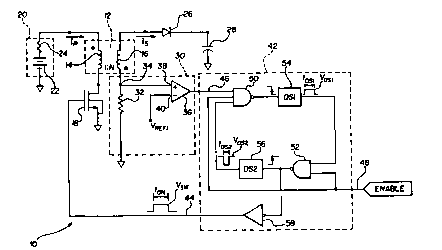
Referring now to Fig. 1, a DC-to-DC
converter 10 of the type known in the art as a
"flyback" converter is shown. The DC-to-DC
converter comprises a coupled inductor 12 having
oppositely wound primary and secondary windings, 14
and 16, respectively. A switching means 18 is
connected in series with the primary winding 14 and
a low-voltage battery 20. Switching means 18 can
comprise for e~ample a MOSFET power switching
transistor or an eguivalent. Battery 20 is shown as
having an open-circuit voltage 22 and an effective
internal impedance, identified by numeral 24,
wherein the effective internal impedance 24 may vary
throughout battery life. A diode 26 is connected in
series to the secondary winding 16 and storage
capacitor 28, for rectifying charging current to
charge capacitor 28. Storage capacitor 28
represents a high-voltage capacitive load.
The flyback converter 10 is constructed and
arranged to charge the capacitor 28 to a ma~imum
voltage of appro~imately 330 volts from the
low-voltage battery 20, which may have a maximum
open-circuit voltage 22 of appro~imately 6 volts.
A current sensing means 30 is connected in
series with the secondary winding 16 to monitor
secondary winding current Is. Current sensing
means 30 outputs a logic "0" (LO) or "1" (HI)
signal, indicative of secondary winding current IS
W O 92~12568 2 ~ ~ 7 4 2 ~ PC~r/US91/09525
being above or below a predetermined minimum
threshold current, IMIN, respectively. The value
of IMIN is selected to provide and achieve optimum
performance of the DC-to-DC converter for the
requirements of a particular application (e.g., a
flyback type self-oscillating flash charger). In
particular, the current level IMIN is selected to
be different from a zero current level. A non-zero
value of IMIN results in improved charge transfer
rates, as well as, improved energy transfer
efficiency. A discussion of the effects of a
non-zero IMIN relating to charge transfer rates
and energy transfer efficiency is found in commonly
assigned U.S. patent 4,272,806.
Current sensing means 30 comprises resistor
32 connected in series with secondary winding 16 at
node 34. Current sensing means 30 further comprises
a comparator 36, wherein a non-inverting input 38 of
comparator 36 is connected at node 34. An inverting
input 40 of comparator 36 is connected to a
reference voltage VREFl. The output of comparator
36 is the output of current sensing means 30.
A controlling means 42 comprises an output
44, and two inputs, 46 and 48. Output 44 connects
to switching means 18 to energize switching means 18
ON/OFF. An ON/OFF signal Vsw on output 44 causes
switching means 18 to enable/disable, respectively,
current Ip to flow in primary winding 14. Input
46 connects to current sensing means 30 to receive
the current sensing means 30 output signal which is
indicative of the secondary current level. Lastly,
input 48 receives a converter charge enable/disable
signal.
Controlling means 42 further comprises two
logic NAND gates, 50 and 52, respectively, two
~097~
WO92/12568 PCT/US9l/~525
one-shot multivibrators,~S4 and 56, respectively,
and an inverting buffer 58. NAND gate 50 comprises
a three input NAND gate. A first input of NAND gate
50 is input 46. A second input of NAND gate 50 is
connected to converter charge enable/disable input
48. The output of NAND gate 50 is connected to a
trigger input of one-shot 54. One-shot 54 is a
negative edge-triggered device, whereby, a negative
going signal transition (i.e., logic ~1~ to logic
"on) from gate 50 causes one-shot 54 output signal
VOSl to change from logic "0" to logic ~1. n
Output signal VOSl remains a logic nln for time
duration toSl. The output of one-shot 54 is
connected to a first input of NAND gate 52. NAND
gate 5Z comprises a two input NAND gate. A second
input of NAND gate 52 is connected to converter
enable/disable input 48. The output of NAND gate 52
is connected to a trigger input of one-shot 56 and
also connected to an input of an inverting buffer
58. The output of one-shot 56 is connected to a
first input of NAND gate 50. The output Vsw of
inverting buffer 58 is connected to switch means 18
via output 44.
Briefly described, the flyback converter 10
operates as follows, making reference to Figs. 1 and
2. Assume that a charge enable signal on input 48
is received by the controlling means 42. Upon
receipt of the enable signal, the controlling means
42 turns switching means 18 ON (Vsw is HI) for a
predetermined time toN (Fig. 2c). With switching
means 18 ON, current Ip flows from the battery 20
through the primary winding 14 of the coupled
inductors 12 (Fig. 2a) and energy is stored in the
inductor primary 14. Current Ip increases (Fig.
2a) in the -inductor primary 14 approsimately in
W O 92/12568 2 ~ 9 7 4 2 I PC~r/US91/09S25
_g_
accordance with the equation:
I _ (Voc/Rtot)(I~e )+nIsMIN
5 Where Ip is primary current;
Voc is open circuit power source voltage;
Rtot is total series resistance of
primary circuit including source internal
resistance, switch transistor ON
resistance, wiring resistance, and coil
resistance;
t is the time measured from transistor turn
ON;
~ is the effective R-L time constant,
Lp/Rtot, where Lp is the value of the
primary inductance;
n is the turns ratio of the coupled
inductors;
Is is secondary current; and
ISMIN is the minimum secondary current
threshold level.
After expiration of time toN, the controlling
means 42 turns the switching means 18 OFF (Vsw is
LO) on output 44, whereby, current Ip in the
primary winding 14 is interrupted (Fig. 2a). Stored
energy in the inductor primary 14 is then
transferred to the secondary winding 16 an~ current
IS (Fig. 2b) begins to flow. Current IS flows
through secondary winding 16, diode 26, and storage
capacitor 28, thus charging capacitor 28. When
current I5 in the secondary winding 16, sensed by
the current sensing means 3Q, decreases below
predetermined minimum threshold current level,
IMIN, current sensing means 30 output changes from
W O 92/12568 2 0 9 7 4 2 1 PC~r/US91/09525
--10--
a logic ~0~ to a logic "1". ~This output signal is
received by input 46 of controlling means 42. The
controlling means 42 then turns the switching means
18 ON again for time toN and the charging cycle
repeats.
Referring now to Fig. 2a, Ipma~ is the
peak primary winding current obtained during a
single charging cycle. During operation of the
converter 10, as the internal impedance 24 of the
battery 20 increases, the peak primary current
IpmaX will decrease accordingly in reference to
the above given equation for Ip. By maintaining a
fised predetermined ON time toN and having a
non-zero secondary current threshold IMIN, we have
achieved a simpler circuit over the prior art for
tracking the converter ~load~ to the power source
internal impedance over the life of the power
source. A discussion of energy transfer efficiency
and battery life performance is found in commonly
assigned U.S. patent 4,272,806.
Upon termination of current Ip in the
inductor primary 14, current IS begins to flow in
the inductor secondary 16. As shown in Fig. 2b,
noise, indicated by numeral 60, is present in
current IS due to reactive parasitic circuit
elements, for example, a parasitic leakage
inductance (not shown) of coupled inductor 12.
Noise 60 makes controlling means 42 susceptible to
prematurely activating switching means 18 via signal
Vsw as indicated in Fig. 2c by numeral 62. The
premature activation would result from current
sensing means 30 detecting current IS decreasing
below the level of ISmin at a time tl (Fig-
2b). The premature activation of switching means 18
would cause undesired deteriorated performance of
W O 92/12568 2 ~ 9 7 ~ 21 PC~r/US91/09525
converter 10. Drive controlling means 42 therefore
includes a means for preventing such a premature
activation of switching means 18, the preventing
means comprising one-shot 56 connected to NAND gate
50.
Controlling means 42 operates as follows.
NAND gate 50 receives three inputs, a first input
from current sensing means 30. Assuming for the
moment that the second and third inputs of NAND gate
50 are at logic ~1" (HI), then the output of gate 50
is dependant upon the output of current sensing
means 30. When the output of current sensing means
30 is logic ~0 (LO), then the output of NAND gate
50 is logic ~1" (HI). The output of current sensing
means 30 is LO when secondary current IS is above
IMIN. Upon secondary current IS decreasing
below IMIN, the output of current sensing means 30
changes from logic ~0" (LO) to logic ~1" (HI) and
the output of NAND gate 50 likewise changes from
logic "1" (HI) to logic "0" (LO).
One-shot 54 receives, as input, the output
of NAND gate 50. As previously mentioned, one-shot
54 is a negative edge-triggered device, whereby, a
negative going signal transition (i.e., logic nl" to
logic ~on) from gate 50 causes one-shot 54 output
signal VOSl to change from logic ~0" to logic ~1"
for time duration toSl. Output signal VOSl is
received as a first input of NAND gate 52. NAND
gate 52 receives a second input from converter
enable/disable input 48, which we have said for the
moment is in a logic "1" state. When VOSl is in a
logic ~1" state and input 48 is in a logic ~1~
state, the output of NAND gate 52 is in a logic ~0"
or LO state. A LO state on the output of gate 52 is
converted into a HI state on the output of inverting
W O 92/12568 2 ~ 9 ~ 4 21 PC~r/US91/09525
buffer 58. The output of inverting buffer 58 is the
output 44 of controlling means 42. As we have
mentioned previously, output 44 provides signal
Vsw to switching means 18. Signal Vsw remains
in the HI state for the time duration toN. During
time duration toN, current Ip flows in inductor
primary 14 and no current flows in inductor
secondary 16. The time duration of toSl of the
logic ~1" pulse of output signal VOSl and
subsequent time delays introduced by NAND gate 52
and inverting buffer 58 make up the time duration of
toN of signal Vsw.
Upon e~piration of time toSl, output
vOSl of one-shot 54 changes state from HI to LO,
causing the output of NAND gate 52 to change from LO
to HI, and causing the output of inverting buffer 58
(i.e., Vsw) to change from HI to LO. Switching
means 18 is therefore deactivated (i.e., turned
OFF). One-shot 56 is a positive edge-triggered
one-shot device and has its input connected to the
output of NAND gate 52. Upon the positive-edge
transition from LO to HI of the output of gate 52,
the output VOS2 of one-shot 56 changes state, from
HI to LO, remaining LO for time duration toS2.
VOS2 is the third input to NAND gate 50. The LO
state in signal VOS2 causes the output of NAND
gate 50 to change from a LO state to a HI state and
to remain HI for the time duration toS2. NAND
gate 50 is therefor prevented from changing its
output state during time duration toS2, that is, a
HI to LO transition is prevented. As a result,
noise 60 in current IS is prevented from
prematurely triggering one-shot 54, and thus
switching means 18. Such a premature trigger signal
is shown in Fig. 2c as indicated by numeral 62, at
WO92/12568 2 0 9 7 4 21 PCT/US91/09525
the point in time indicated by tl. Because of the
LO presented by signal VOS2 on the third input of
NAND gate 50, the output of current sensing means 30
has no effect on the output of gate 50.
Time duration toS2 is selected to be
longer than the time duration of noise 60. For
e~ample, noise 60 has been found to be approximately
200xlO 9 seconds in duration. Time, toS2, is
thus selected to be longer than the time duration of
noise 60, say for example, 450xlO 9 seconds.
The second input to NAND gate 50 is
connected to controlling means input 48. Input 48
represents a converter enable/disable signal line.
That is, when a logic ~l" (HI) appears on input 48,
drive controlling means 42 is enabled, NAND gate 50
receives a logic ~l" at its second input, and the
converter operates as previously discussed. When a
logic "0" (LO) appears on input 48, drive
controlling means 42 is disabled, NAND gate 50
receives a logic "0" (LO) at its second input, and
converter lO is disabled. A logic "0" on the second
input of gate 50 inhibits gate 50 from changing its
output, regardless of a HI or LO state on the first
and third inputs. As a result, converter lO is
effectively disabled. Enabling or disabling
converter lO is desirable to control the amount of
voltage stored on capacitor 28. A voltage sensing
means (not shown) on capacitor 28 could provide a HI
or LO signal corresponding to the voltage on
capacitor 28 being below or above a predetermined
value, respectively.
In an alternate embodiment shown in Fig. 3,
DC-to-DC converter lO is similar to that shown in
Fig. l with the following differences. Controlling
means 42 further includes one-shot 64, digital
20~742 i
WO92tl2568 PCT/US91/09525
-14-
multiplexer (MUX) 66, and additional toN select
input 68. The output of NAND gate 50 is connected
to the trigger inputs of both one-shot 54 and
one-shot 64. One-shot 64 is a negative
edge-triggered device, whereby, a negative going
signal transition (i.e., logic "1" to logic ~on)
from gate 50 causes one-shot 64 output signal VoS3
to change from logic "0" to logic "1. n Output
signal Vos3 remains a logic "1" for time duration
toS3. Time duration toS3 corresponds to the ON
time toN2 of output signal Vsw of controlling
means 42. Similarly, toSl corresponds to the ON
time toNl. Time duration toS3 (toN2) is
longer than time duration toSl (toNl), as will
be discussed subsequently. The output of one-shot
54 is connected to a first input 70 of digital
multiple~er 66. Likewise, the output of one-shot 64
is connected to a second input 72 of digital
multiple~er 66. The output of digital MUX 66 is
connected to the first input of NAND gate 52. Input
68 (toN select) connects to a select input of
digital MUX 66; whereby, a logic ~o" (LO) on input
68 causes the output of one-shot 54 at first input
70 to appear on the output of MUX 66. Similarly, a
logic ~1" (HI) on input 68 causes the output of
one-shot 64 at second input 72 to appear on the
output of MUX 66. Although only two toN
selections have been shown, it is to be understood
that a plurality of toN selections may be
implemented in a similar manner as described.
The current sensing means 30 of DC-to-DC
converter 10, as shown in the alternate embodiment
of Fig. 3, further includes an analog multiple~er 74
having first and second inputs 76 and 78,
respectively. First and second inputs 76 and 78 are
WO92/12568 2 0 9 7 4 2 1 PCT/US91/09525
-15-
connected to reference voltages VREFl and VREF2,
respectively. Reference voltage VREFl corresponds
to an IMIN current level of IMINl. Likewise,
reference voltage VREF2 corresponds to an IMIN
current level of IMIN2. Reference voltage VREF2
is greater than VREFl, corresponding to IMIN2
being greater than IMINl as will be discussed
subsequently. Current sensing means 30 further
includes an IMIN select input 80. Input 80
connects to a select input of analog MUX 74;
whereby, a logic "0" (LO) on input 80 causes V
to appear on the output of MUX 74. Similarly, a
logic In (HI) on input 80 causes VREF2 to appear
on the output of MUX 74. The output of MUX 74 is
connected to the inverting input 40 of comparator
36. Although only two IMIN selections have been
shown, it is to be understood that a plurality of
IMIN selections may be implemented in a similar
manner as described.
The alternate embodiment of Fig. 3 operates
similarly to the preferred embodiment of Fig. 1 with
the following differences. Input 68 of controlling
means 42 is used to select a predetermined ON time,
t or t A logic n o~- (LO) on input 68
selects toNl whereas a logic "1" (HI) on input 68
selects toN2. The predetermined ON times, toNl
and toN2, can correspond to the type of battery or
batteries used (e.g., toNl for 3 volt (AA or AAA
size) Alkaline batteries, toN2 for a 6 volt
lithium battery, etc.). In this manner, the
controlling means 42 and the converter 10 are easily
adaptable for use with different types of
batteries.
In a similar manner as noted above, the
input 68 of controlling means 42 can be used to
W O 92/12568 2 ~ 9 7 ~ 2 1 PC~r/US91/09~25
-16-
select one of several predetermined ON times,
wherein, the ON times vary in duration (i.e., t
is less than toN2, etc.). In this manner, the ON
time of the charge cycle can be varied within the
lifetime of a particular battery (or set of
batteries) in order to improve "late-life" charging
performance. As a result, optimum performance of
converter 10 can be achieved throughout the life of
the battery.
The alternate embodiment of Fig. 3 further
operates wherein input 80 of current sensing means
30 is used to select a predetermined minimum
secondarY current level, IMINl or IMIN2. A
logic ~o n (LO) on input 80 selects IMINl; whereas,
lS a logic ~1~ (HI) on input 68 selects IMIN2. The
predetermined IMIN levels, IMINl a MIN2
can correspond to the type of battery or batteries
used (e-g-, IMINl for 3 volt (AA or AAA size)
alkaline batteries, IMIN2 for a 6 volt lithium
battery, etc.). In this manner, converter 10 is
easily adaptable for use with different types of
batteries.
In a similar manner as noted above, the
input 80 of current sensing means 30 can be used to
select one of several predetermined IMIN levels,
wherein, the IMIN levels correspond to different
threshold levels (e.g., IMINl is greater than
IMIN2, etc.). In this manner, the IMIN level of
the charge cycle can be varied within the lifetime
of a particular battery (or set of batteries) in
order to improve "late-life~ charging performance.
As a result, optimum performance of the converter 10
can be achieved throughout the life of the battery.
There is thus provided a DC-to-DC converter
which provides substantial advantages over the prior
W O 92/12568 2 ~ 9 7 ~ 2 1 PC~r/US91/09525
-17-
art, that is, a simple, cost effective, and high
energy transfer efficient DC-to-DC converter.
Furthermore, there is provided a DC-to-DC converter
having improved battery life performance, improved
charging performance, and high noise immunity. The
high noise immunity further provides improved
converter reliability.
While the invention has been particularly
shown and described with respect to the certain
preferred embodiments thereof, it will be understood
by those skilled in the art that the foregoing and
other changes in form and detail may be made therein
without departing from the spirit and scope of the
invention.