Note: Descriptions are shown in the official language in which they were submitted.
2097~
CO~ECTOR AS8EMBI,Y AND METNOD Ol? M2~TIFACTURE
This invention relates to an electrical connector
assembly and method of manufacture, particularly for a
miniature UH~ coaxial connector~
In U.S. Patent 5,088,937, there is disclosed a
right-angle coaxial jack connector having an outer
metallic shielding and grounding shell containing a
coaxial transmission path for ultra high frequency
signals with the shell including parts that fit together
to seal the connector against contamination and
radiation. The shell and cooperating metal parts
minimize radiation from signal energy carried by the
connector and interference with signals carried by the
connector by radiation external to the connector as well
as providing a grounding function for circuits connected
by the connector. The various parts that form the shell
include elements that prevent internal contamination by
flux, solder products and the like, when the connector
is soldered to a printed circuit board as part of an
assembly for electronic apparatus. The patented jack
connector includes relatively fine posts extending from
the rear bottom thereof that are fitted into holes in a
printed circuit board to be soldered thereto to effect
the grounding connection of the shell that serves as a
shield. The shell and associated parts are typically
formed by die casting zinc or zinc alloys which elements
are then trimmed to prepare the exterior surfaces for
the necessary plating to control oxidation of the
connector. Typically, the parts are washed, scrubbed,
mechanically or chemically, and then plated with various
platings including tin, nickel, gold, or, in certain
occasions, silver, these various platings being combined
to prevent migration of the zinc constituents through to
the surface of the outside plating. Most typically, the
parts are barrel plated requiring a tumbling in the
plating operation with considerable mechanical stress to
15313 CA
~. . .: :, ., ., : : : , ,
, ,: , . .
7 8 ~ ~
the parts. It has been discovered that the most
frequent loss of elements is during the tumbling
operation and/or handling or subsequent assembly of the
parts, particularly the small posts that are made
integral with the shell.
Accordingly, it is an object of the present
invention to provide a connector construction that
facilitates manufacture, including plating and assembly,
with minimum damage to the fine posts utilized to solder
a connector shell to a printed circuit board or the
like. It is a further object to provide an improved
construction and method relative to the prior art in
making electrical connectors.
It is a still further object to provide an improved
UHF-type connector assembly and method of manufacture.
The present invention achieves the foregoing
objectives by providing a ~onnector having a relatively
heavy grounding shield shell ~ormed as by die casting of
zinc or zinc alloys to include in the rear an opening
facing rearwardly and downwardly from the bottom of the
shell. An insert is formed to close the rear o~ the
opening of a separate element and a relatively
lightweight base element, typically formed as by die
casting, is provided to close the bottom portion of the
opening by an Pngagement with the shell. In a preferred
embodiment, the shell opening is made to have internally
~acing grooves that receive the outside edges of the
insert element in a sliding engagement to position the
insert in khe opening with the posts for the connector
formed on the insert extending downwardly from the shell
bottom. Next, the dielectric insert and signal contact
is installed. The back insert is positioned in place
last with the bottom insert base in position to lock the
back insert in position with shell edges coined to keep
the back insert in place. The invention contemplates a
reversal of the receiving grooves and projections so
15313 CA
that the insert base includes grooves and the shell
inrludes projections. The invention also contemplates
that the connector may have insert bases with posts of
different sizes or posts on different centers to
accommodate different footprints on printed circuit
boards to thus allow a more efficient manu~acturing
operation for a family of connectors. The small fine
posts, being formed on a relatively light piece, can be
separately treated in a manufacturing process including
barrel plating with a minimum loss by fracture or
breakage of the posts, compared to prior art practices
wharein the relatively large heavy assembly contained
the integral posts.
A coaxial conn ctor assembly comprising a metallic
shell having a central bore and a rearwardly disposed
cavity, a dielectric insert disposed along the central
bore and having an interior bore extending therethrough,
an electrical contact having a contact section disposed
along the interior bore of the insert and termination
section extending exteriorly of the shell, a rear insert
secured in a back end of the shell, another dielectric
insert disposed in the cavity through which the
termination section extends. A contact insert is
mounted onto the shell along the cavity and the other
insert and includes termination members extending
outwardly therefrom.
The invention will now be described by way oE
example with reference to the accompanying drawings in
which:
Figure l is a perspective, showing elements in an
exploded arrangement prior to assembly viewed from the
rear and underside of the connector assembly.
Figure 2 is a side, elevational, and partially
sectioned view of the elements of Figure 1 fully
assembled.
15313 CA
~7~9~
"~
Figure 3 is a rear, elevational view of the
assembly of elements of Figure 2.
Reference is made to the aforementioned U.S. Patent
5,0~8,937 for a description of one type of connector
served by the present invention through a modification
of the assembly and an improved method of manufacture
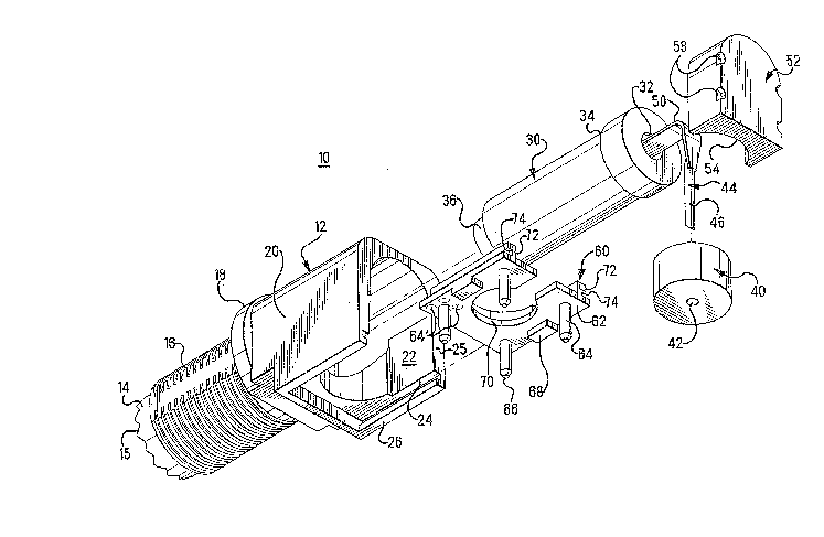
therefor. Referring to Figure 1, an electrical
connector assembly 10 is shown to include a grounding
and shielding shell 1~ having a forward sleeve portion
14 with teeth as at 15 intended to mate with a mating
connector that engages assembly 10. The f`orward end of
the connector includes threads as at 16 that mate with
the interior threads of the mating connector and a
flange 18 that serves to provide a stop for such
engagement. Shell 12 includes a rear portion 20 that
has an interior cavity 22 that opens from the rear
defined by walls 25 and to the bottom defined by walls
26 to extend through the shell as indicated in Figure 2.
As can be discerned from Figure 1, the walls 26 each
include interior grooves 24 having a function to be
described hereinafter. The side profile in section of
the shell 12 can be seen in Figure 2 to include an
interior offset 28 that serves as a stop positioning a
di~lectric insert 30 within the cavity 22 that can be
seen to extend from the rear through shell 12. The
dielectric insert 30 includes an interior bore 32 that
extends therethrough, an enlarged outer diametex portion
34 that engages offset 28 to position the insert within
shell 12, and a reduced diameter portion 36 in the
forward end thereof. A further dielectric insert 40 is
provided that fits up within the bottom aperture of
shell 12 in an insert 60 for purposes to be described.
Note in Figures 1 and 2 that insert 40 includes a
central aperture 42 that receives a portion of the
signal contact. The contact 44 includes a downwardly
extending leg or post 46 and, as shown in Figure 2, a
15313 CA
' ' ' , ~ :. :: ~ '
2~7~3~
forward portion 4~ that i~ a receptacle contact adapted
to receive the signal pin contact of a mated connector
fitted therewithin. As can be seen also in Figure 2~
the contact 44 includes a bent portion 50 more or less
coaxial to the interior space within 22~ Figures 1, 2,
and 3 show a further insert 52 with rounded interior
surface 54 (Figure 1~ and of a con~iguration to fit
within the complementary interior of shall 12 defined by
a rear flat face 25 of such shell~ The rounded surface
54 serves with other portions of the shell to define an
essentially coaxial path. Energy propagated through the
connector following the signal contact 44 is transmitted
in part through the dielectric including insert 30, the
air space surrounding the ends of insert 30, and the
dielectric insert 40.
As can be seen in Figure 3, the insert 52 includes
edge reliefs 58 that may be utilized to lock the insert
52 axially to the shell 12 by a slight deformation of
the edge of the material of 25, a deformation just
sufficient to effect the lock without fracturing the
plating of the shell. Alternativelyr solder or other
means may be utilized to lock insert 52 to shell 12.
The insert shown as 60 in Figures 1-3 is comparatively
small and light relative to the shell 20. Insert 60
includes a lower, or bottom, face 62 having a number or
relatively fine posts 64 extending therefrom, rounded as
at 66 to facilitate an insertion of the posts within the
holes of a printed circuit board and adapted to be
soldered to such holes and traces contained within such
holes to electrically and mechanically lock the
connector shell to the printed circuit board and serve,
in certain instances, as a partial mounting for the
connector. As is shown in Figure 1 through the phantom
circles 64', it is contemplated that the posts 64 may
have other positions, three exemplary positions for one
post being shown. The invention contemplates different
15313 CA
2~7895
size posts being used that shown with some of the posts
of the larger diameter or greater or shorter length than
other posts to fit the particular packaging concept
being employed. Insert 60 includes projections 68
extending from surface 62 that serve as standoffs,
holding the surface 62 slightly above the printed
circuit board to allow a cleansing following soldering
of any material that might be trapped under the face 6~.
Insert 60 includes at the outside edges projections 72
grooved as at 74 of a dimension and geometry to fit
within the grooves 24 adjacent a lower surface 26 of
shell 12. This engagement is shown in Figures 2 and 3.
In accordance with the invention, different inserts
60, having differently centered posts or different si~es
of posts, may be manufactured for use with the same
shell 12 and other assembly elements to thus complete a
family o* connectors adaptable to fit different
footprints on printed circuit boards of electronic
assemblies. Insert 60 includes a central aperture 70
including a slot 71 at the trailing edge of the insert.
As can be seen in Figures 2 and 3, the connector is
assembled by pre-install`ing a contact 44 in inserts 30
and 40 and fitting inserts within shell 12 following
installation of insert 60 in the bottom with insert 52
then positioned by sliding the insert in the rear of
shell 12. Thereafter, insert 52 is locked in place as
shown in Figures 2 and 3 and secured to the shell to
lock the assembly together.
The invention fully contemplates a reversal of
projections and grooves with respect to insert 60 and
shell 12 or other means of attaching the insert to the
shell. When the assemhly 10 is completed, the signal
path represented by contact 44 and the surrounding
plastic and dielectric material is essentially sealed
from radiating outwardly, assuming a mating connector is
engaged with the front end of the shell and that that
15313 CA
. - ~. . . , :,
:- :, ~: : : ~
2~7$~
- 7
connector is mounted on a printed circuit board. Thus,
signals representing unwanted radiation exterior to
shell 12 cannot by induction alter the signal being
carried by the connector, and signals propagat~d by the
connector cannot be radiated externally to cause
problems with related circuits or equipment. Also note
that the connector, when assembled as in Figures 2 and
3, is essentially sealed so that contaminants cannot
migrate or *ind their way into the interior volume of
the connector to cause an alteration in impedance,
shorting, or the like. The connector assembly 10 can be
so manufactured, assembled and shipped and utilized as
an integral assembly.
In accordance with the invention in a preferred
embodiment, the shell 12, insert 52, and insert 60 are
manufactured by die casting of 7inc or zinc alloys with
a subsequent slight trimming of flash as by tumbling or
by hand, washing or a treatment for plating with the
insert 60 separately plated as by barrel plating without
risk of the relatively heavy loads of shell 12 causing
post breakage.
The invention thus provides a connector assembly
useful for handling ultra-high frequencies, frequencies
on the order of 1 or 2 Ghz, and a method of
manufacturing that facilitates handling and processing
of elements that are relatively small and fine and
fragile, compared to the shell portions of the
connector.
15313 CA
2~n78~S
ADYANTACES OF TH~ INVE~TION
An advantage of the present invention is a separate
contact insert having termination contact members
thereon that is removably inserted into a metallic shell
of an electrical connector so that the shell can be
separated, cleaned, and plated from the contact insert
thereby preventing damage to the termination contact
members. Another advantage of the present invention is
a radiussed inner surface of ~ back closure insert
mounted on the metal shell to better define a coaxial
path along a curved section of the electrical contact.
15313 CA