Note: Descriptions are shown in the official language in which they were submitted.
2098358
~ 1
The present invention relates to optical
telecommunication systems, and more particularly it
concerns an optical switch for fast cell-switching
networks.
Fast cell ~or packet) switching technique, also
called ATM from the initials of the designation in the
English language "Asynchronous Transfer Mode", is
becoming more and more important for switching digital
flows at very high rates, such as the flows present in
the digital broadband integrated service networks. In
this technique, the information relevant to the various
services is organized into adjacent units with a fixed-
length (about 400 bits), called "cells", comprising an
information field and a header field, carrying the
connection identifier together with other service
information.
Due to the rate and bandwidth requirements by
integrated service networks, the use of optical
technologies is acquiring an increasing interest in the
realization of both transmission lines and switching
function. At the present state of technique, however,
optical technologies do not allow high processing
capacities, and the optical switching systems generally
proposed provide the use of an electrical control part
2098358
(therefore with a high processing capacity) and of an
optical transport part (with a high capacity of
information flow throughput). Examples of these networks
have been described, for example, in the European Patent
Applications EP-A-0 224 244 and EP-A-0 411 52 and in the
papers: "A Photonic Knockout Switch For High-Speed Packet
Networks", presented by K. Y. Eng at the IEEE/IEICE
Global Telecommunications Conference 1987, 15-18 November
1987, Tokyo, Japan; "Optical Technology Application to
Fast Packet Switching" presented by P. Cinato and A. de
Bosio, at the Topical Meeting on Photonic Switching, 1-3
March 1989, Salt Lake City, USA; "Electro-Optical
switching node based on fast packet and frequency
switching techniques", presented by A. de Bosio et al. at
the International Switching Symposium, May 1990,
Stockholm, Sweden.
Electronic control units however have operating
speed limits which could prevent full exploitation of the
optical part capabilities because they compel to limit
the bit rate on the input lines to the node.
The aim of the invention is to provide an optical
switch allowing to fully exploit the capacity of the
optical components, and which utilizes hence information
flows at a very high rate within it, though in the
presence of an electronic control part.
According to the invention the switch comprises an
interconnection optical network, an electrical control
network, termination devices associated to each switch
input and to each switch output, splitting information to
be forwarded to the electrical control network from the
information to be processed in the interconnection
network, and recombining into the cell flow the
information coming from the control network and from the
interconnection network, and means for the time
compression of signals to be switched and the time re-
expansion of switched signals, and is characterized in
that:
- each input of the interconnection network is associated
2098358
to means forming cell aggregates by associating a
plurality of cells which must follow the same path
through the interconnection network, and performing
said time compression by acting on the aggregates, so
as to form information units the duration of which is
equal to a predetermined fraction of the original
duration of an aggregate and the information contents
of which, as number of bits, is equal to the sum of the
information contents of the aggregate cells;
- the electrical control network manages the switching,
through the optical interconnection network, at the
cell aggregate level; and
- each output of the interconnection network is
associated to means for said time expansion, in order
to bring the aggregates outgoing from the
interconnection network back to the original duration,
and to separate the individual cells before forwarding
them on the output lines.
Time compression of packets to be switched through
an optical switching network is known in sé from Patent
No. 1217130 granted in Italy in the name of the Applicant
itself, in which, however, individual packets are
compressed made up of electrical signals, which are
converted into optical form after compression.
The switch is preferably an ATM digital cross-
connect system and the aggregation and compression means
form cell aggregates relevant to the same virtual path.
The application of the invention to a cross-connect
system is useful because the traffic to be switched is
sufficiently high to allow the formation of cell
aggregates without introducing excessive delays.
The invention will be better understood with
reference to the annexed drawings, wherein:
- Fig. 1 shows the general structure of a switch
according to the invention:
- Fig. 2 shows the structure of the cell aggregation and
compression units:
- Fig. 3 is a schematic diagram of the compression
4 20983S8
operation;
- Fig. 4 shows the structure of the decompression units;
- Fig. 5 is a schematic diagram showing the
decomp-ression.- - -
By way of a non limiting example, the invention is
described with reference to an ATM digital cross-connect
system comprising an optical switching network and an
electronic control network. As it is known an ATM cross-
connect system switches ATM flows at a virtual path
level. A virtual path is generally asssociated to
semipermanent calls, so that a cross-connect system does
not require very frequent re-configurations; this is a
typical application where, after configuring the
switching network, throughput of a large quantity of
traffic must be guaranteed, and it is therefore important
that electronic control units should not set any
constraint.
According to the invention, this is obtained thanks
to the presence of cell flow processing units, inserted
on one side between the line and exchange termination
devices providing re-synchronization, extraction of ATM
flows from any transmission synchronous supports, label
conversion at a virtual path level, conversion into
electrical form of the signalling information to be
supplied to the control units, etc. and the inputs of the
switching network, and inserted on the other side between
the outputs of the switching network and the termination
devices providing the complementary operations required
for inserting the cells again on the transmission
carriers.
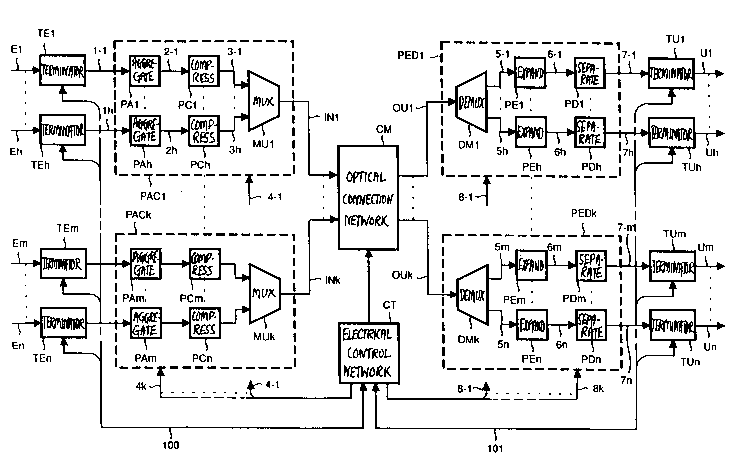
In Fig. 1 the optical connection network is
indicated by CM, the electrical control network by CT and
the line and exchange termination devices respectively
associated to input optical connections El...Eh...Em...En
and to the output connections Ul...Uh...Um...Un by
TEl...TEh...TEm...TEn, TUl...TUh...TUm...TUn.
The termination devices TE, TU are well known in the art
and they are not part of the invention and this is why
2098358
they will not be described in detail. A possible example
of realization is anyhow described in EP-A-0 411 562.
Outputs 1 (1-l...ln) of the devices TE are connected
to units PACl...PACk, each of which receives the cells
outgoing from one or more devices TE. In the drawing, in
particular, the outputs of the devices TEl...TEh are
connected to PAC1 and those of the devices TEm...TEn to
PACk. The number of lines connected to the units PAC is
the same for all these units.
The units PAC comprise, for each of their input
lines:
- means PA (PAl...PAh...PAm...PAn) forming cell
aggregates relevant to the same virtual path, and
joining to each aggregate a label, valid inside the
lS cross-connect system, to allow management of aggregates
by the control units CT in the same way as the
individual cells are usually managed in an ATM switch.
- means PC (PCl...PCh...PCm...PCn), performing a time
compression of the bits inside the aggregates present
on output 2 (2-1....... 2h... 2m... 2n) of the relevant
aggregation device, by reducing the duration of each
aggregate by a preset factor C.
When the number k of the inputs/outputs IN, OU in
the connection network CM is lower than the number n of
the inputs/outputs E, U of the switch, as shown in the
example, each unit PAC includes also multiplexer MU
(MUl...MUk) cyclically scanning the outputs 3
(3-1...3h...3m...3n) of all the compression means PC and
concentrating the compressed aggregates on these outputs
onto an input line IN (INl...INk) to the CM switching
network. Control signals for multiplexers MU are supplied
by the system time base, which is part of the control
units CT, through the proper connection wires 4-1...4k,
schematizing as a whole the connections for signal
exchange between units PAC and control units CT.
In a typical example of realization, the cross-
connect system can present 512 input/output links E/U and
use a switching network CM (with 64 inputs/outputs; each
2098358
input link can convey cells related to 10 virtual paths;
the aggregates (having the same ~;mensions) can comprise
from 8 to 16 cells.
As a result of the aggregation and compression
information units are obtained with a duration
substantially equal to that of a cell but with contents
equal to the sum of the contents of all the cells of an
aggregate, and they convey therefore a much greater
quantity of information in the time unit. The electronic
control units CT will process these information units
instead of the individual ATM cells and they will hence
not have any special speed requirements and will not set
any constraints to the optimal exploitation of the
optical switching network. The fact that cell aggregates
are to be processed instead of individual cells does not
imply any modification in this control unit, the
structure of which is therefore analogous to that already
proposed for some prototypes of ATM switches. As a
consequence of aggregation and compression, there will be
a proportional increase of the necessary bandwidth, which
requires the use of an optical technology for switching
network CM.
Time compression factor C (which can be of the same
order of magnitude as the number of cells forming an
aggregate) will preferably not be lower than the ratio
n/k between cross-connect system inputs and CM connection
networks inputs: in this way guard times between
aggregates can be left to make connection network
operations easier.
This becomes specially important if a cell and frequency
switching is carried out in the cross-connect system, as
described in the mentioned paper by A. de Bosio et al.
and in ~P-A-O- 411 562.
Outputs OUl...OUk of the switching network CM are
connected to demultiplexers DMl...DMk, belonging to
respective units PEDl...PEDk which perform inverse
operations of the units PAC. Each demultiplexer DM has
one input and as many outputs as the inputs of a
209~358
_ 7
multiplexer MU. - -
Outputs 5-1...5h...5m...5n of demultiplexers DM are
connected to respective means PEl...PEn for the time
expansion of the aggregates, followed in their turn by
means PDl...PDn for the decomposition of the aggregates
into individual cells. Means PD receive from means PE the
aggregates to be decomposed through the respective
connections 6-1...6n, eliminate the additional label and
supply the individual cells on connections 7-1...7n
towards the devices TUl...TUn. As the number and the
position of the bits making up the label are known and
the cells have a constant length, the person skilled in
the art has no difficulty in realizing a device capable
of performing the required functions: e.g. the units PD
can be suitably timed registers.
Units PED receive the proper control signals from
the control units CT through connections 8-1...8k. Units
PAC, PED are the processing units for the ATM cell flow
which are the subject of the invention.
In the preferred embodiment which will be described
hereafter, cell aggregation is carried out on electrical
signals, and compression and concentration operations are
carried out on optical signals. Similarly, expansion is
carried out optically and decomposition of aggregates in
electrical form. Since connections E, U are supposed to
be of an optical type, termination devices TE, TU will
incorporate the required optical-to-electrical conversion
devices and vice versa. This is not an additional
complication for the switching system structure since
these conversion devices are provided in any case when
optical flows on input/output lines are organized as
usual according to the standard synchronous digital
hierarchy (SDH), because SDH frames are processed in an
electrical form. Connections 100, 101 schematize the
connections between termination devices TE, TU and the
control units CT.
Fig. 2 shows a possible embodiement of units PA, PC.
Unit PA mainly consists of a bank of FIFO memories
2098358
(10 in the example considered) MFl...MFp, each of which
organizes a queue of cells relevant to the same virtual
path to form aggregates. Considering that memories
receive cells at random, the writing/reading control
units must be able to recognize the preset number of
cells has been written and, once this number is reached,
to start reading even if any cell to be inserted in a
successive aggregate is still being written. To avoid
excessive delays, reading must start in any case after a
maximum preset time is out even if the aggregate is not
complete. This m~ximllm time will be counted by a suitable
counter, provided in the control units of the memory
itself and started when the first aggregate cell arrives,
by using clock signals supplied by the time base of the
electrical control network CT by means of wire 40
belonging to one of the connections 4 in Fig 1. For
drawing simplicity, said control units are incorporated
into the blocks MF; memories organized to allow these
operating procedures are well known in the art.
A label valid within the cross-connect system
(containing service information in general and
information about the aggregate characteristics in
particular) will also be added at the head of each
aggregate; the label is supplied by TE through the
25 relevant connection 10-110p (which is part of line 1
in Fig. 1) and is loaded into the memory when the arrival
of the first cell of an aggregate is recognized. This
label will generally be used by the decomposition units
PD. Service labels of this type are created by the units
TE also in the case of conventional ATM cross-connect
systems (e.g. that described by A. L. Fox et al. in the
paper "RACE BLINT: a technology solution for the
broadband local network", presented at IEE Conference on
Integrated Broadband Services and Networks, October 1990,
London).
Cells to be stored come from TE, through a
connection 11 (which is also part of line 1) connected to
the input of a decoding network DE presenting ~ outputs
20983S8
g
respectively connected to memories MFl...MFp. Through
connection 12, DE receives from TE, as control signals,
the label bits of each cell arriving to TE (and therefore
the bits of the label which has not undergone conversion
yet) which identify the virtual path and, according to
such label, it routes the cell towards the proper memory
MF .
The outputs of memories MF are connected to the
inputs of a selector SL the output of which is output 2
of block PA. The selector must act in synchronism with
multiplexer MU, and more precisely it must transfer an
aggregate to its output at an instant such that, taking
into account the time required for compression, the
aggregate is present on output connection 3 of the
concerned block PAC at the moment when MU is scanning the
connection itself. The aggregate which SL must transfer
to the compression units PC will be the or an aggregate
ready in one of the memories MF (e.g. the first one
completed) or the or an aggregate for which maximum hold
time in memory has already expired. The selector will
then be associated to a control logic LC receiving from
control units of the individual memories MF signals
indicating that an aggregate has been formed or that the
preset time has expired.
Alternatively the different selector inputs can be
cyclically scanned.
It is to be noted that data will be generally
written and read in parallel (e.g. on 8 bits) in
memories MF. Considering that compression units, as it
will later be better examined, must act on one bit at a
time, devices for the parallel-to-series conversion of
the information flows must be provided. In the drawing,
these devices have been incorporated into block SL, which
will receive the necessary timing signals from the time
base through connection 41. Obviously serialization could
be carried out upstream of SL.
The formation of aggregates of 8 - 16 cells, as
supposed by way of example, allows a significant
2098358
~o
reduction of the number of information units to be
processed in CM without increasing remarkably the delay
across the cross-connect system.
The necessity of limiting the delay advices to use
the invention at the level of a cross-connect system
because at this level the traffic concerning a virtual
path will be sufficiently high to allow reaching in
relatively short times the number of cells desired for an
aggregate.
Anyhow, in theory, the invention could be used in
any switching node, by forming cell aggregates which have
to follow the same path in the connection network CM.
Serialized aggregates, consisting of bit strings
where each bit has the same duration and period as the
bits of the cells present on connections E, are supplied
to the bit time compression unit PC.
The unit PC comprises:
- a mode locked laser LA, generating a succession of
pulses with a duration much lower than that of the bits
present on connection 2 and a period equal to the bit
time To of these bits;
- an electro-optical amplitude modulator MD, which
receives the pulses from laser LA and the signal
present on connection 2, and in which each bit of this
signal modulates the pulses outgoing from laser LA with
an on/off modulation; in this way an optical signal
consisting of a succession of bits having a duration
which is equal to that of the pulses emitted by LA and
a period To is obtained on connection 5;
- a succession of c elements RPl...RPc (with 2C= C), each
of which effects the folding on itself of the bit
string relevant to an aggregate, halving its duration
each time. As indicated for RP1, each element RP
comprises an input coupler A1, sharing the power
associated to each optical bit between two different
paths, and an output coupler A2 recombining the signals
coming from the two paths. An output of the input
coupler A1 and an input of the output coupler A2 are
2098~58
11
directly connected and form one of the two paths; the
second path is obtained by connecting the second output
of A1 to the second input of A2 through a delay element
R which causes the bits in the second half of the
5 aggregate to be arranged interleaved with the bits of
the first half in the output coupler A2. If y is the
number of bits in each aggregate, this is obtained if
the delay element R in the first folding element RP1
introduces a delay of (y-1) To/2 with respect to the
signals sent along the other path, that of the second
folding element RP2 introduces a delay of (y-l)To/4,
etc.
In general, the delay element of the i-th folding
element RPi will introduce a delay (y-l)To/2i.
AS a consequence of the forwarding of the bits of an
aggregate on two paths and of the successive
recombination, at the output of each folding element
RP1 . . . RPC each aggregate will be associated to a replica.
Hence each element RP will be followed by a unit,
20 schematized by switches SWl...SWc, which will be operated
to eliminate this replica, as it will better be seen
further on. These switches are controlled by signals
supplied by the control units through connections
43-1...43c, which are part of the proper connection 4 in
25 Fig. 1. Units such as SWl...SWc are well known in the
art, and hence further information is unnecessary.
On output 3 of unit PC there is therefore a
succession of aggregates with an overall duration yTo/2C
and period yTo. From the foregoing description it can be
clearly seen that once the compression factor is
established, it is immediate to determine the instant of
the exit of the aggregates from memories MF in such a
manner that the aggregates reach multiplexer MU within
the time devoted to that particular line 3. During the
interval between two aggregates, multiplexer MU will
forward on line IN the compressed aggregates supplied by
the other units PC of the same block PAC.
Compressed aggregates on lines IN are then switched
20983~8
12
inside CM with the procedures required the particular
network.
It is to be noted that at the instant when an
aggregate is forwarded to the switching network CM, the
line exchange and termination devices TE will forward to
the control unit CT-the necessary routing information: as
a matter of fact these should not undergo compression as
the control unit would not be able to read them.
Operation of unit PC is shown in Figures 3a-3e
considering by way of example the case of an aggregate
with y = 8 bits to be time compressed by a factor C = 4;
two foldings are therefore required.
Fig. 3a shows schematically the aggregate to be
compressed, formed by bits the duration of which is
substantially equal to period To. Figure 3b shows the
aggregate converted into optical form, with bits having a
strongly reduced duration and period To, arriving at
input of coupler A1 of RP1 and propagating towards A2
without undergoing delays in RP1. The delay element R1 of
RP1 introduces a delay 7To/2 by giving the sequence in
Fig. 3c: as it can be seen, bit 1 outgoing from R1 occurs
at half the interval between bits 4 and 5 of the non
delayed sequence (and therefore at the central instant of
the duration of the aggregate); bit 2 outgoing from R1
occurs at half the interval separating the arrival of
bits 5 and 6 of the non delayed sequence, etc. At the
output of RP1 (Fig. 3d), an initial group of bits (bits
1-4 of the non delayed aggregate) is followed by a
sequence of bits in which the bits of the second half of
the original aggregate are interleaved with those of the
first half, and this sequence is still followed by a
queue of bits consisting of bits 5-8 of the delayed
sequence. Bit time is T1 = To/2. The initial group (head)
and the queue, indicated as a dashed line in Fig 3d, must
be eliminated and for this purpose switch SW1 must be
closed for a time substantially equal to yTo/2 (duration
of compressed aggregate) starting from the instant when
the first bit of the aggregate exits from the delay
2098358
_ 13
element R of folding element RP1: considering as instant
0 that when the aggregate to be compressed arrives at the
input of RP1, the closure of SW1 must substantially take
place after a time 7To/2.
In the successive folding element RP (RP2), the
delay element introduces a delay equal to 7To/4, i.e. 7/2
of the bit time of the aggregate already compressed by
RP1: the first bit of the delayed sequence will reach the
input of the output coupler A2 at half the interval
separating bits 6 and 3 of the non delayed sequence (and
therefore again in correspondence with central instant of
the duration of the aggregate). In this way the bits in
the second half of the aggregate are interleaved again
with those of the first half of the aggregate that is
entering into the element. At the output of the second
folding device the sequence shown in line 3e is obtained,
with a duration equal to 1/4 of the original one. Also in
this ca~e it will be necessary to eliminate by means of
the : W~ ...,.l following RP2 the head (bits 1, 5, 2, 6, of
the non delayed sequence) and the queue (bits 3, 7, 4, 8
of the delayed sequence) of the bit flow outgoing from
RP2: neglecting the propagation time between the output
of SW1 and the input of RP2, SW2 will be closed for a
time equal to yTo/4 starting from an instant that follows
by 7To/4 the arrival of the first bit of the non delayed
sequence. These head and queue are not shown any more in
Fig. 3e.
If C > 4 (and hence c > 2) the operations are
repeated identical in the successive folding units and
after ~ folding, the bit period will be Tc=To/2C
Comparing lines 3b, 3e, it can be seen clearly that
the signal present at the output of a unit PC consists of
very short sequences of bits which occupy only a fraction
1/2C of the original duration of the aggregate. This
explains the use of multiplexer MU (Fig. 1), which
inserts into the unused time the compressed aggregates
relevant to other input lines of the same unit PAC.
Referring to Fig. 4, cell aggregates present at
2098358
.
14
output 5 of a demultiplexer DM (Fig. 1) are supplied at
the input of an expander ES which has C outputs and are
transferred simultaneously on C lines 50-1...50C, which
terminate at the inputs of the respective gates
CAl...CAC, sampling with period To the bit strings
present on the respective line 50. Control signals for
gates CA are supplied by the control units CT through a
line 80 which is part of one of the connections 8 in Fig.
1. Also the realization of gates such as gates CA is well
known in the art, and hence further information is
unnecessary. Lines 50 have lengths which are different
and progressively increasing from line 50-1 to line 50C
and so they introduce a progressively increasing delay on
the signals conveyed. For what concerns the invention,
the interest lies in the relative delay between one line
and the line preceding it, which must be equal to the
period Tc of the compressed bits. The minimum delay (line
50-1) can therefore be considered as equal to 0, while
the generic line 54j (j=l...C) will introduce a delay
(j-l)Tc.
Outputs of gates CAl...CAC are connected through the
respective lines 60-1...60C to an integrator-detector IR
which effects an integration in the time of the bits
received and their conversion into electrical form, so as
to reconstruct the cell aggregates corresponding to those
outgoing from blocks PA (formed therefore by bits with
period and duration To). In practice IR will be made up
of a unit reconstituting the bit sequence and of an
optical-to-electrical converter. Lines 60 have also
different lengths, in order to introduce different delays
on the bits that conveyed. The delay introduced by each
line is a multiple of the overall duration y.Tc of a
compressed aggregate and it is progressively increasing,
by steps of y.Tc, from line 60C to line 60-1. More
particulary, the delay will vary from 0 (line 60C) to
(C-l).y.Tc (line 60-1) and, for the generic line 60j, it
will be (C-j).y.Tc. The reasons for the choice of the
given values for the delay introduced by lines 50, 60
20~83~8
_ 15
will appear clearly from the description of the operation
of unit PE, with reference to Fig. 5.
Here the e~pansion of the 8-bit aggregate compressed
by a factor C = 4 as shown in Fig.3 has been shown by way
of example. Fig. 5a shows the situation of the aggregates
on lines 50-1...50-4 at the input of the sampling gates
CA, Fig. 5b the situation on lines 60-1...60-4 at the
output of the same gates. The first sampling pulse CK0
for the aggregate being examined reaches gates CA at the
moment when bit 1 of the aggregate is present at the
input of gate CA connected to line 50-4; due to the
various delays introduced by lines 50-2...50-4 with
respect to line 50-1, at the same instant bits 7, 5, 3
are present respectively on lines 50-1, 50-2, 50-3, the
second sampling pulse CK1, which arrives after time To =
4Tc, lets bits 8, 6, 4, 2 pass at the outputs of gates
CAl...CA4: on the four lines 60 four distinct pair of
bits, each comprising bits that were adjacent in the
original aggregate, propagates towards the integrator.
The bits of each pair are spaced by the original bit
time. Line 60-4 is the one with the least delay and
therefore bit 1 is effectively the first bit reaching the
input of integrator IR. The immediately preceding line
60-3 introduces a delay of 8Tc (= 2To), and therefore,
before a bit present on this line reaches integrator IR,
this receives bit 2 from line 60-4. After a time 2To
passes, IR will receive bit 3 followed by bit 4, and so
on; The original sequence of the bits has therefore been
reconstituted at the input of IR. Integrator IR will
then bring each bit back to its original duration and
convert it into electrical form, giving the sequence in
Fig.5c, which reproduces exactly the one present at the
input of a unit PC.
It is to be noted that the above described expansion
scheme requires the overall length of the aggregates to
be a multiple of compression factor C. This does not
constitute a limitation because it is sufficient to
choose suitably the number of cells in the aggregate, if
2098358
l6
the length of same does not satisfay this condition.
It is clear that what described has been given only
by way of non limiting example and that variations and
modifications are possible without going out of the scope
of the invention. So, for example, multiplexers MU can be
replaced by passive combining devices, receiving in a
sequential way the compressed aggregates outgoing from
one group of compression units PC. Obviously, the
demultiplexers DM will be then replaced by complementary
passive distribution units. In this case it will be the
time base to establish the reading instant of the various
aggregates in memories MF so that they arrive at the
inputs of the multiplexing unit with the required
sequence.
Moreover, the folding elements RP could be realized
so as to form a number of replicas of the aggregate
different from 2, e.g. 3, 5, etc..., obtained by delaying
the input aggregate of multiples of To/3, To/5 ...., so
that compression ratios will be obtained which are powers
of 3, 5, etc. In this case, if z is the number of
replicas formed, the delay element R constituting the
x-th path inside the i-th element of the succession of
folding elements will have to introduce a delay of
(x-l)(y-l)To/zi on the signals that run across it.