Note: Descriptions are shown in the official language in which they were submitted.
~N9-92-1()5 - 1-
MULTI-MEDIA ANALOG/DIGITAL/OPTICAL SWITCHING APPA~ATUS
.
FIELD OF THE INVENTIONS
The inventions relate to multi-stage networks comprised of switching
apparatus devices, and particularly to ability to send digital, analog, or
optlcal slgnals through the network equally well.
The inventions also relates to digitai computer systems comprised of several
or many computing and/or input/output elements, and the ability of the said
individual elements lo perform high speed, low-latency communications with
each other in a parallel fashion equally well over digital, analog, or opticai
slgnals all encompassed in a single network.
BACKGROUND OF THE INVENTIONS
In the fleld of parallel processing, the ability of fast and parallel
communication amongst processors workin~c1 on the same task is an
important consideration. It is also important to be able to transmit data of
various types, such as digital, analog, and optical efficiently amongst
processors.
This application is directed to parallel processing, parallel switchingnetworks, and particularly to an improved adaption of serial fiber or analog
wire transmission media to parallel switching networks for the purpose of
interconnecting large numbers of processors with a minimal interface. The
processors can be interconnected to form a shared processinJ resource - a
"farm" of processors - to provide either massive joint computional power for
a single task or individuai processors assignable to individual tasks.
Corporations are beyinning to view this type of nfarm" approach as being
very valuable. Individual workstations can be purchased and given to
:, ' .'', ;' ' ' ' ` ' '
L N9-92- los - 2 ~ J~ :~
individual employees to supeort their work effort during the day. However, in
the evenings or on weekends, the workstations are networked together to
form a massive processing base for performh~g batch jobs or paraliel
processiny. Industry is becoming aware that massive processing power can
be obtained at a lower cost by investing in less expensive workstations,
rather than in the traditional single large mainframe processor.
The state-of-the-art switches do not effectively meet the requirements of the
versatile "farm" systems. First, they are inflexible and dictate that a single
homogeneous serial transmission media and protocol be employed
throughout the entire system. Secondly, they are generally switching
systems designed to switch high bandwidth serial transfers or analog
transmissions without regard for latency. They attack only half the problem
in that they provide parallel data communication, but the~ do not provide for
parallel path set-up through ~he switch. Therefore, they do not provide a full
parallel network capability. Instead, all network paths share a central matrix
controller function that operates in serial. If a processing node wishes to use
a path through the switch, it must first arbitrate for the facilities of the central
matrix controller. The matrix controller services one request at a tirme,
causing parallel requests to wait their turn. The central matrix controller
acknowledges one switch set-up request at a time. It receives a short
message indicating the switch connection desired. The central matrix
controller checks a matrix map stored in the central matrix controller's
memory and determines whether the requested connection can be
established or not. If it can, the central matrix controller sends a command
to the switching element (usually referred to as the switch fabric) to make the
requested connection. Then the cenlral matrix controller responds to the
requesting node telling it whether the desired connection has been rnade or
is not available. Th~ processlng node then uses the established connection
and transmlts data to or from the desired destination through the switch
fabric, while the central matrix controller works on establishing the next
serial connection. The processing node must go through a similar procedure
to break the switch fabrlc connection using the central matrix controller, when
.. . . . ..
l~ Ns-92- l ()5 - ~ "
it is finished using a given switch path. Thus, the latency of the central
matrix controller approach in regards to establishing and breaking switch
paths is very poor. In existing prociucts, this type of approach has been
adequate connect DASD's and other l/O devices to computer complexes, or
to send batch information between processors. These types of applications
transfer long disc records or large batch data at a high bandwidth. The poor
latency is amertised over the large transfer and has a small effect on the
overail performance. However, this is not the case for the modern "farm"
approach, where messages can be short and latency becomes as important, if
not more so, as bandwith. Harold S. Stone in his book "High- Performance
Computer Architecture" (Addison-Wesley 1990, pg.309) states that the
performance benefits of parallel processing depends strongly on the ratio
R/C, where R is the run-time of the processing (the computational work to be
done3 and C is the communication overhead required amongst n parallel
processors jointly working on the job. The value C includes latency as well
as bandwidth, and to keep C small and make parallel processing efficient, the
switch latency must also be kept small.
Thirdly, another drawback of the central matrix controller switching approach
is the limited number of processors that a single central controller can
manage. Systems ilave been built to interconnect 8, 16, 32, and possibly as
many as 64 processors, but that appears to be approaching the the limit of
the concept. The central matrix controller approach also has a reiiabiltiy
problem in that a failure in the central controller can fail the entire
communication system and render the whole parallel system useless.
We have solved some of the problems encounterecl h1 the prior art which we
referred to above. A distributed switch controller approach, rather than a
centralized approach, appears to be a better solution for parallel processing
because of its inherent low latency, its ability to withstand failures, and its
ability to expand to interconnectin~ massively parallel systems. The
distributed and fully parallel switch utilized herein to solve the ~arm"
interconnect problem efficiently is the ALLNODE Switch (Asynchronous, Low
,
-' ' ' ~ : '
l~ N9-92- 105 4 - ~J~ ~ t~
Latency, inter-NODE switch), which is described in N U.K. Published
Application No. 92101705.9, dated September 30, 1992 and adapted by the
present invention to per~orm the switching of serial data lines at low latency
and hi~h bandwidths. The ALLNODE switch provides a circuit switching
capability at high bandwidths similar to the switch fabric in the central matrixcontrolled switches; however, the ALLNODE switch includes distributed
switch path connectlon set-up and tear-down controls individually within each
switch - thus providing parallel set-up, low latency, and elimination of centralpoint failures. We will further describe in the detailed description a way
whereby the ALLNODE switch and the present invention can be used to solve
the "farm" problem effectively.
This application builds on the basic ALLNODE Switch which is adapted by the
present invention to perform the low latency switching of
analog and optical data lines, as well as standard digital data lines.
SUMMARY OF THE INVENTIONS
The invention is a switching apparatus for interconnecting muitiple
processors or other functionai elements and enabling the said elements to
send digitai, analog, or optical signals between any two elements. The media
is fully parallel and supports n such transmissions simultaneously, where n is
the number of functional elements interconnected by the switching network.
Any of the n simultaneous transmissions can be digital, analog, or optical i
any proportion.
The switching means is an expansion o~ the basic digital asynchronous and
unbuffered switching concept embodied in the ALLNODE Switch. The
ALLNODE switch permits connection control and data transfer between
elements to occur over a common and small set of point-to-point, digital,
Interconnecting wires. The present inventions expands this digital base to
not only be used for digital 1ransmissions, but to also be expanded to serve
.
. . . . . . . . .. . .
1,Ns-92-1()s - 5~ c~ h ~
as a distributed controller for the purpose of controiling analog, optical, or
any other type of transfer between elements of the system.
The invention apparatus has many near term applications7 such as the
switching of common analog based signals including TV signals, radar
scanners, modem outputs, telephone lines, etc. from a single source to any
node of the system including different processors, 1/0 devices, or displays.
The analog links can also accept ser)al digital protocols which are not in the
form used by the basic swltching apparatus; these protocols can be
transmitted as is without revision throuyh the analog switch and allow
heterogenous systems to comrnunicate via serial digital transmissions over
the analog paths. In addition, the switching apparatus can also be used as a
distributed switch controller to control optical and other types of non-digital
switches .
The invention apparatus ~urther provides a switching network communication
structure that has the characteristic of simplicity of implementation, and does
not require data buffering or data conversion of any kind. It establish0s or
breaks connectlons multiple connections (digital, analog, optical, etc.)
instantaneously and Is, therefore~ dynamlcally changeable with a very quick
response tlme. It has the capabllity of resolvlng requests to establish
connections in a parallel manner, where N connections can be established or
broken at the same tlme (where N = the number of elements of the system
which are communicatlng via the switching network). Thus, the number of
connections that can be made or broken simultalleously scales directly with
the size of the system. This capability enables the invelltion apparatus to
handle multiple short messages very efficienily. In addition, the new
apparatus is devoid of synchronization requirements or wire length
restrictions. It also has the ability to track the speed improvements of new
technologles and to increase performance as the technology used to
implement the invention apparatus improves.
. . . . . . . . . . .
.. , :,:: , . . . . .
IiN9-92- 105 - ~
In addition, the new switching apparatus can be cascaded with other identical
invention apparatus devices to form interconnection networks among any
number of system eiements or nodes. Said network wouid have the
characteristics for full parallel interconnection.
BRIEF DESCRIPTION OF THE DRAWINGS
FIGURE 1 illustrates generally our preferred embodirnent of the presentinvention of a Multi-Media Analog/Digital/Optical Switching apparatus, which
has the capability of interconnecting multiple analog, digital, and optical
channels through a parallel switching network.
FIGURE 2 illustrates a four input and four output (4 X 4) crossbar switching
apparatus, which has the capability of providing the discloseci fully parallel
switching means for interconnecting analog and digital signals for up to four
nodes.
FIGURE 3 illustrates the interconnections required to a four input and four
output (4 X 4) crossbar switching apparatus to provide full interconnection
amongst four nodes.
FIGURE 4 shows a typical method for cascading the 4x4 disclosed
embodiment of the invention swilching apparatus to accomodate systsms
having more than 4 nodes.
FIGURE 5 shows a schematic block diagram of the simple digital data flow
and control path implementations of the 4x4 crossbar switching apparatus,
which has the capability of being used with the present invention to provide
fully parallel switching means for interconnecting up to four system nodes for
the purpose of 1ransferring digital data.
.,, ,. . .. . . . ,. ,. ~,
. : .... .. . , . .. . . ,.. . . . ~ . ... ..
I~ N9-92- 1()5 ~ ~3 ~ ~ {~
FIGURE 5A shows a schematic block diagram of the simple data flow and
control path implementations of the 4x4 disclosed embodiment of the
invention switching apparatus to provide for the routing of analog signal
through the invention switching apparatus.
FIGURE 6 illustrates a typical method ior ~enerating parallel control and and
multiple line serial dlgital data information to be sent to the 4x4 prior parentembodlment of the invention switching apparatus over four synchronous data
llnes.
FIGURE 7 shows a typlcal timing diagram for routing the digital interface
signals arriving at one input port of the 4x4 prior parent embodiment of the
invention switching apparatus to one output port.
FIGURE 8 illustrates the typical method of selecting and establishing atransmission path through a network comprised of the invention switching
apparatus for the purpose of sending digital data from one node to another.
FIGURE 9 illustrates the typical method of implementing the analog
multiplexers used by the present invention to switch analog signals through
the disclosed switching apparatus.
FIGURE 10 illustrates a typical method for using the parent embodiment of
the invention switching apparatus for implen1enting a distributed controller
~unction for high speed optical switches.
DETAILED DESCRIPTION OF THE PREFERRED EMBODIMENTS
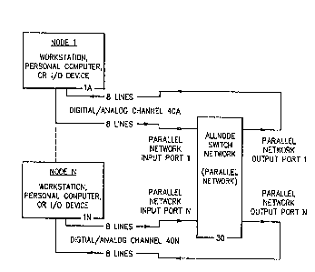
Turning now to the drawings in greater detail, as illustrated by FIC;URE 1,
showing the preferred method of interconnecting N nodes via digital and
analog data channels connected to a parallel multi-stage switching network
I ,N9-92- l ()5
comprised of the present invention switching devices. Each node 1 oF a
parallel system can ~e comprised oF a workstation, personal computer,
mainframe CPU, or any l/O device, such as a DASD. A typical node 1A
connects to the parallel network over a proprietary digital and analog data
channel 40A, which is herein disclosed.
The preferred embodiment uses only unidirectional interfaces, and therefore
Flgure 1 shows the dlgital and analog data channeis 40A to be comprised of
two unidirectlonal lines, one carrying data frorn node 1A, and one carrying
data to node 1A. It is possible for any node to send digital or analog data to
any other node through switch network 30. For example, node 1A could send
a digital message or analog waveform into network 30 by using data channel
40A. Every transmission of digital and/or analog data to the network 30 must
include a digital control header, which is used to command the switch
network 30 to make the connection to the requested destination node (node
1N in our example). Switch network 30 forms the requestecl connection and
then digital messages and/or analog waveforms can flow through network 30
frorn 1 node to the selected destination node In similar fashion any node
can communlcate with any other node through network 30.
.
Referrlng to Figure 2, the preferred embodiment is a 4x4 switching apparatus
12, where the function of the present invention is to provide a means of
connecting any of 4 sets of digital, analog, or optical inputs on a mutually
exclusive basis to any one of the unused 4 output ports. The 4x4 switching
apparatus 12 can support up to 4 simillltaneous connections at any given
time. For instance, Input 1 could be connected to Output 3, input 2 to Output
4, Input 3 to Output 2, and input 4 to Outpul 1.
The invention switching apparatus 12 is unidirectional, which means that data
flows in only one direction across the said switching apparatus 12, that being
from Input to output. Switching apparatus 12 interfaces are ciefined in detail
in Flgure 2. The set of lines 31, 32, 33, anci 34 at each in-port to the switchlng
apparatus 12 are identical in number and function to the set of lines 41, 42,
.
. .
- : , . ~ . . . :
.
.. . .
~N9-92-1()s - ')- .~
43, and 44 at each out-port. The sets of interface lines to each input and
output port contain seven + Y unique signals: 4 digital data lines, 3 digital
control lines (VALID, REJECT, and ACCEPT~, and Y signals carrying analog
data. The signals at each port are differentiated by a pre~ix of INX- or OUTX-
indicating the direction and number of the port (X) that 1hey are associated
with. The four digital data and one VALID lines and Y analog iines have a
signal flow in the direction going from input to output across switching
apparatus 12, while the digital REJECT and ACCEPT control !ines have a
signal flow in the opposite direction.
The Switch Interface requires only 8 signals, as shown in Figure 2, to transmit
and control digital and/or analog data through the network 30 -- the digital
data and control transfer width is 1/2 byte (4 bits) at a time. The signals
required are:
DATA: 4 parallel signals used to command switch connections
and transmit digital data messages or digital control headers.
VALID: When active, indicates that a digital message, control header, or
analog waveform is in the process of being transmitted. When
inactive, indicates a RESET command and causes all
switches to reset to the IDLE state.
REJECT- Signal flow is in the opposite direction from the
DATA and VALID signais. When active, it indicates that a REJECT
or error condition has been detected.
ACCEPT: Signal ~low is in the same direction as the REJECT signal.
When in the low state, it indicates that a message is in the
process of being received and checked for accuracy. When active,
it indicates the message has been received correctly.
ANALOG Y - Is a single analog signal or a group of Y analog signals that
';,
~, . . ., , ": . .
. .
,' ' , ' . ~ ~ . ; . ' ',:
-,:,, ' ,, ' :., . ' : '., ~ . .
.
I N9-92-105 ~ 9 3 ~ 2 ~
carry unidirectional analog waveforms in lhe same direction as the
DATA and VALID signals through the invention switching apparatus.
Fi3ures 3 to 8 refer to a 4X4 crossbar implementation of the ALLNODE Switch
to illustrate the principles and speed of the switching concept.
As illustrated by FIGURE 3 the ALLNODE switching apparatus would be
provided for a node having a plurality of input and output ports, and would
comprise the connection control circuit for each input port, and a multiplexer
control circuit for each output port for connecting any of I inputs to any of Z
outputs, where I and Z can assume any unique value greater or equal to two,
as in the parent application.
Figure 3 shows a 4x4 crossbar ALLNODE switching apparatus, where the
ALLNODE switching apparatus 10 is unidirectionai, which means that data
flows in only one direction across the said switching apparatus 10, that being
from input to output. Although the said switch apparatus 10 is unidirectional,
it supports bidirectional communication amongst four nodes (20, 22, 24, and
26) by connecting the 4x4 ALL-NODE switching apparatus 10 as shown in
FIGURE 3. Each node 20, 22, 24, and ~6 has two sets of unidirectional
interconnecting wires, one going to the switch 10 and one coming from the
switch 10. The dashed lines internal to the switching apparatus 10 indlcate
that the function of the said switching apparatus is to connect an input port
such as INPUT PORT 1 to one of four possible output ports. The switching
apparatus 10 provides exactiy the same function for each input port, allowing
it to be connected to any unused output port.
Referrin~ to Fl(3URE 4, a method is illustrated for increasing the number of
nodes In a system by cascading eight switching apparatus 10 blocks. The
elght cascaded switches are denoted as 10A through 10H to indicate that they
are identical copies of switching apparatus 10, varying only in regards to the
wlring of their input and output ports. It can be noted that any of sixteen
nodes can communicate to any other node over a connection that passes
. .
I~ N9-92- 105
through exactly two of the switching apparatus 10 blocks. For instance, Node
5 can send messages to Node 15 by traversing switch 10B and switch 10H.
Since all connections are made through two switching apparatus 10 blocks,
the network comprised of the eight switching apparatus 10 blocks is referr~d
to as a two stage switching network. Other multi-stage networks can be
configured from switching apparatus 10 blocks by using three stages, four
stages, etc. in a slmilar manner.
Referring to FIGURE 5, a functional diagram of the simple data flow across
ALLNODE switching apparatus 10 is illustrated. The VALID and four data
lines at each input port, inside the switch, and at each output port are
represented by a single line in FIGURE 5 for simplicity. For instance, the
VALID and four data lines entering switch 10 at IN PORT 1 go to five internal
functional blocks of switching apparatus 10; these are blocks 50A, 60A, 60B,
60C, and BOD. Block 50A makes the decision as to which of the four possible
output ports are to be connected to input port 1. The VALID and four data
lines from each input port go to each output multiplexer block (60A, 60B, 60C,
and 60D); this makes it possible to connect any input port to any output port.
Each of the four output multiplexer blocks (60A, 60B, 60C, and 60D) is
uniquely commanded from each of the control blocks (50A, 50B, 50C, and
50D) as to which of the four possible sets of input port lines is to be gated
through to each output port. For instance, control block 50A can command
mu1tiplexer 60C to connect input port 1 to output port 3; control biock ~OB can
command multiplexer 60A to connect input port 2 to output port 1; and
control block 50C can command multiplexers 60B and 60D to connect input
port 3 in a multi-cast fashion to output port 2 and output port 4 All three
connections are capable of being established simultaneously or at different
times. At the same time that multiplexers 60A to 60D ~orm connections to
move the VALID and data signals across switch 10 with a unidirectional
slgnal flow from input port to output port, multiplexer 61D and AND gate 63D
form si0nal connections for the REJECT and ACCEPT signals, respectively,
with a slgnal flow In the opposite direction of output port to input port (typical
implementations are shown by blocks 61 D and 63D -- sirnilar blocks are
., .
, ~ , ' . ~ .
I~Ns-92-los - 12- ~ 2 '~
associated with each input port). These REJECT ancl ACCEPT signals provide
a positive feedback indication to switch 10 of actions taken either by
subsequent switch 10 stages in a cascaded network or by ihe device
receiving and interpreting the VALID and folJr data signals. A control header
or digital message being transmitted through switching apparatus 10 over the
four data si~nals under control of the VALID signal can be REJECTed by any
network stage if it is unable to establish the commanded connection or by the
receivin~ device if it is not capable of receiving the message at this time or if
it detects an error in the transmission. The receiving device also has the
capability of confirming the correct arrival of a command or message (without
errors being detected) by pulsing the ACCEPT signal. Since the REJECT and
ACCEPT signals go in the opposite direction from the data flow, they provide
a means of reporting back a positive indication to the sender on whether the
attempted transmission was received correctly or rejected.
Referring to Figure 5A, it is shown how the parent invention of Figure 5 is
expanded to implement the present invention by adding analog ou1put
multiplexer blocks 65A, 65B, 65C, and 55D to each switch output port. The
analoy Y lines from each input port go to each analog output multiplexer
block (65A, 65B, 65C, and 65D); this makes it possible to connect any input
port analog slgnals to any output port analog signals. Each of the 4 analog
output multiplexer blocks (65A, 65B, 65C, and 65D) is uniquely commanded
from each of the control blocks (50A, 50B, 50C, and 50D) by the exact same
signals that command the 4 digital output multiplexer blocks (60A, 60B, 60C,
and 60D). This makes an analog selection of which of the 4 possible sets of
input port analog Y lines are to be gates through to each output port. For
instance, control block 50,9 can command multiplexers 60C and 65C to
connect input port 1 to output port 3 both, control block 50B can command
mulfiplexers 60A and 65A to connect input port 2 to output port 1, control
block 50C can command multiplexers 60D and 65D to connect input port 3
output port 4, and control block 50D can command multiplexers 60B and 65B
to connect input port to output port 2. All four connections are capable of
being established simultaneously or at different times. Note, that i1 is
~ : ,.' " ' ' '
: .
I N9-92-105 - I~ 2 ~
possible to combine both analog and digitai rnultiplexers in the same chip
and produce a single chip capable of perronning both tasks. Either a digital
message or analog waveform being transmitted through switch 12 can be
REJECTED by any switch 12 stage, if it is unable to establish the commanded
connection, or by the receiving device if it is not capable of receiving the
message at this time or if it detects an error in the transmission.
Rsferring to Figure 6, biocks 56, 5Z, and 54 illustrate a typical method for
generating multi-line (parailel)/serial digital data in the form Or a message
which can be transmitted to and across switching apparatus 14, which is a
partial drawing of the switching apparatus 12. Similar parallel/serial data
generation logic as provided by 56, 52, and 54 can be used at each o~ the
other input ports to switching apparatus 12. Each set of input data lines
provides 4 serial data lines to a given input port which is synchronized to the
same clock by the four shift registers 54 which create the parallel/serial data
by shifting four synchronized lines of data 31 as controlled by the same
identlcal clocking signal (100 MHZ in Fig.6). However, the four different input
port sources (31, 32, 33, and 34) to switching apparatus 14 can b0
asynchronous to each other, being based on different, non-synchronized, 100
MHZ clocking signals.
The process for sending parallel/serial messages through switching
apparatus 14 involves FIFO 56, which accumulates data messages to be
transmitted. The next entire message to be transmitted is moved to buffer 52.
The message stored in buffer 52 is moved to shift registers 54 in preparation
for transmittal and the data is dispersed across the four shift registers 54 by
placing data bit 0 into the first bit of shift regisler 1, da!a bit 1 into the ~irst bit
of shift re0ister 2, data bit 2 into the first bit of shif~ register 3, data bit 3 into
the flrst blt of shift register 4, data bit ~I Into the second bit of shi~t register 1,
etc. Shift registers 54 then begin to send serial data to switching apparatus
14 over four synchronized data lines, in such a manner that the parallel/serial
data flows continuously until the entire message has been transmitted. The
switch apparatus 14 uses the first eight bits transrnitted (in the first two clock
.. .. ... . . . .. . . . .
, . ~ ,
, , . ,. ,. . ... :
rN9-92-los - 14~
cycles of serial data over interface 31 from serial registers 54 to switching
apparatus 14) to select and establish a connection path through the switching
apparatus 14. The example in Figure 6 iilustrates via dashed lines, the
switching apparatus establishing a temporary connection between input port
1 (31) and output port Z (42), such that each of the eight individual lines in
Interface 31 are uniquely anci directly connected to each of the corresponding
lines in interface 42.
Referring to Figure 7, typical serial waveforms are shown for both input and
output ports of the switching apparatus 14. The switch removes the first 8
bits of the serial transmission as sent by shift registers 54 and uses them to
make and hold a connection, such as interface 31 to interface 42. The
remainder o~ the serial message in our example is transferred directly from
Interface 31 to interface 4Z, so that interface 42 sees that exact same
message that interface 31 receives, minus the first 8 bits and delayed by the
circuit delays encountered by the serial data as it traverses the switching
apparatus 14. Switching apparatus 14 does not buffer or re-clock the serial
data entering via interface 31 in any manner; it merely reflects as quickly as
possible the input waveforms it receives over inter~ace 31 to output interface
42 without changing them in any way, except to strip off the first 8 bits.
The convention for indicating to a switch 14 input port over an interface (such
as 31) that there is no transfer in progress, is to issue continuous IDLE
commands, which are denoted by the 4 data lines and the VALID control line
being held at logical O's. The detection of a logical 1 on any of the input lines
will signify the departure frorrl the IDLE state and signify to the switch that a
selection and transfer is beginning. Likewise, the outpuf lines from the switch
will be held in the IDLE state (at all O's), when there is no active transfer inprogress.
In general, all switches require a path selection method, whereby they are
commanded which connection (input port to output port) to establish. For
switchin~ apparatus 10, the path selection command is transmitted to the
' ' ', , '. ' ,.. ", ' ~ '
I~N9-92-]05 - 15-
switch over the same inter~ace that the data is transferred; i.e., the 4 data
lines associated with each input pnrt. Selection information nlust be
transferred prior to the data, so that the commanded interconnections can be
established and the data can then flow to the commanded destination. The
selection information need NOT identify an input port number (1 to 4),
because it is arriving at the switch over a speci~ic input and the switch
already knows what input number it is receiving data on. Therefore, the
selectlon Information need ONLY specify the number (1 to 4) of which one of
the four output ports of switching apparatus 10 to which to connect. The
method of path selection recommended here is one out of N encoding with a
return to zero (called a DEAD FIELD).
Referring to Figure 8, a typical example of the exact serial bit patterns and
control signal activation is shown for sending control and digital data
information to switching apparatus 10. The example references the cascaded,
two stage switching network shown in Figure 4 and involves sendin~ data
across the network from node 1 through switching apparatus 10A and 10F to
node 7. To make this connection, input port 1 must be connected to output
port Z of the first stage switching apparatus 10A, and input port 1 must be
connected to output port 3 of the second stage switching apparatus 10F. The
signal sequence that is sent to input port 1 to cause the desired connections
in switching apparatus 10A and 10F is shown in Fig. 4. In the signal
sequence of 1's and 0's, time advances from left to right, so that the values
seen at clock time -2 arrive at switch 10A first, and the values at clock time -1
arrive second, etc. The values of the IN1-DATA and IN1-VALID lines are all
zeroes and cause nothing to happen at switch 10A during times -~ and -1,
because they indicate IDLE. At clock time 0, the IN1-VALID line goes to a
logical 1. This prepares switch 10A by enabling the input port 1 to receive
data, but no connection or action takes place at switch 10A at this time. The
IN1-VALID control line basically enables the corresponding switch input port;
when IN1-VALID is a logical 0, switch jOA cannot make any connections or
receive any data from input port 1, which is held RESET. Finally, at ciock
, ,:, -: , : . , :
r.Ng-92-los - ~ 2 ~
time 1, switch 10A receives its command as to what output port to connect to;
the command is received entirely during clock time 1.
The command bit pattern sent at clock time 1 is used by switch 1 OA to
establish connection to an output port; this process is referred to as a path
selection operation and iakes place completely internal to switch 10A. The
path selection approach implemented by the present ALL-NODE switch
invention is to let each of the 4 IN1-DATA lines to define a unique output of
switch 10A to be selected. For instance, IN1-DATA1 signal going to a logical
1 at time 1 tells switch 10A to connect to output port 1, IN1-DATA2 commands
connection to output port 2, etc. In our example, since IN1-DATA2 goes to a
loyical 1 during ciock time 1, switch 10A is thereby commanded to connect to
output port 2. In other words, the connection algorithm is that the first data
input line going to a logical 1 after an input port has been enabled, defines
the connection which that input port is to make. This is a mutually exclusive
process, in that for the normal case only one data line at clock time 1 is
allowed to be a logical 1; the other 3 data lines must be O s. Note that since
1 bit of selection information is guaranteed to be a !ogical 1, switch 10A will
be able to recognize the start of a transmission without requiring any
additional bits to signify that a transfer is commencing. The switch 10A
makes the commanded connection by removing the 4 bits ~rom lhe data lines
and storing them in a se!ection register in control block 50A of Figure 8. The
bits transmitted during clock time 1 are not passed through switch 10A to
switch 10F, but instead switch 10A begins passing the very next 4 bits of data
corresponding to clock time 2 to the next switch 10F. However, the
-. information bits following a selection command (those transmitted by the 4
. data lines at clock time 2 in our exarnple) must always be all zeroes (a DEAD
FIELD) as shown in Figure 8. The purpose of this will be explained
subsequ0ntly.
At clock tlme 2, the connection of switch 10A input port 1 to output port 2 is
established and causes the signal sequence at clock time 2 to be transrnltted
across switch 10A and the interconnecting wires to switch 10F input porl 1.
.
.. . . .
. :, . , : ' ' , ' ,
EN9~92- 1()5 - 17 - ~ L,~ ~
From this time on, switch 10A mereiy transmits all subsequent data
immediately to switch 10F input port 1; it never examines or takes any action
on any other data patterns presented to switch 10A over its input port. 1
interface. ît just passes ail data patterns it receives over input port 1
immediately to the output port 2 and switch 10F. Thus, at clock time 2,
assuming zero delay across switch 10A and its associated cable, switch 10F
Input port 1 sees the VALID signal rise and the all zeroes DEAD FIELD orl the
4 data lines coming into swltch 10F input port 1. In this way, at time 2, switch10F input port 1 is enabled in an identical manner to the way switch 10A
input port 1 was enabled previously at time 0.
In our example, IN1-DATA3 goes to a logical 1 during clock time 3 and switch
10F is thereby commanded to connect its input port 1 to its output port 3, in a
manner similar to the way switch 10A was commanded to connect its input
port 1 to its output 2 during clock time 1. The switch 10F in making the
commanded connection, removes the 4 bits at clock time 3 from the data
lines, and stores them in the selection register which is part of control block
50A of Figure 5. The bits transmitted during clock time 3 are not passed
through switch 10F to Node 7, but instead switch 10F begins passing the very
next 4 bits of data corresponding to c1Ock time 4 to Node 7. However, the
information bits folîowing a selection command (those transmitted by the 4
data lines at clock time 4 in our example) rnust always be all zeroes (a DEAD
FIELD) as shown in Figure 8. Thus, by clock time 4, switches 10A and 10F
have established a connection path for transferring data directly from Node 1
to Node 7. Up to clock time 5, Node 7 sees nothing but IDLE commands. At
time 4, Node 7 sees the OUT3-VALID line from switch 10F go active and is
thereby enabled to start receiving data at time 5. From thne 5 on, Node 7
can receive data from Node 1 over the 4 OUT3-DATA lines from switch 10F.
The protocol of the actual data being transmitted can be any of the normal
formats such as manchester encoded, 8/10 bit encoding with preamble, etc.
However, the preferred embodient, as shown in Figure 8 is an all ones
synchronization field at time 5, followed by the NRZ data message. The data
message can specify the word count length of the transfer. The purpose oF
.. . .. . .
- ,: , , . ~: .: .............................. .
. ~. . : , , . .. . . ~ .
. . . : , . :, . .. , . ~ ...
1~ ~19-!~2- 105 - I ~ -
the synchronization field of all ones as a prefix to the actual data message, isto enable the receiving node 7 to synchronize to the sending node 1 in one
clock time. This assumes that the tW3 nodes involved in the data trans~er
have clocking systems that are asynchronous to each other, but are operating
at the same frequency within a specified tolerance.
The preferred embodiment is to transmit the word count length of the
message first during clock time 6 and clock time 7. Node 7 then decrements
tile length count and can detect when the transfer is complete. Node 7 can
then check the message for accuracy using the selected error detection
method (parity, ECC, or CRC). If the message has been received correctly,
Node 7 responds by activating the ACCEPT interface line back to switch 10F
at clocktimes n~1 and n+2. Switch 10F passes the ACCEPT indication back
to switch 10A, which in turn returns it immediately to Node 1. This indicates
to Node 1 that the transfer completed successfully, and Node 1 resets its
VALID and 4 data lines to switch 10A to zeroes, thus, completing the data
transfer and returning to the IDLE state. The IN1-VALID input line to switch
10A going to a zero at time n+3, causes switch 10A input port 1 to break its
connectlon to output port 2 and to return to the IDLE state. Imrnediately,
switch 10F sees its IN1-VALID input line go to a zero, breaks its connection to
output porl 3 and returns to the IDLE state. Thus, the connections can be
broken and the switches returned to IDLE in as little as one clock time. If
Node 1 has another message to transmit, it can load the next message into
buffer 52 and shift registers 54 (Figure 6), and begin transmission to Node 7
or any other node as soon as time n+4. The only restriction is that the
VALID signal generated by Node 1 must return to zero for a minimum of one
clock time (time n+3) to signify the end oi one transfer before beginning
another.
If Node 7 finds an error in the message it has received after the word count
has gone to zero at clock time n, it responds by activating the REJECT
Interface line (instead of ACCEPT) back to switch 10F. Switch 10F uses the
incoming REJECT signal from Node 7 to break its connectlon to Node 7, to
:' , ', ' '. ' -; ' . . . . :
.
EN9-92- 105 - 19 -
return to the IDLE state, and to pass the REJFCT indication back to switch
10A, which in turn returns it immediately to Node 1 after breakin0 its
connections and returning to IDLE. Node 1 then notes that the transfer has
been rejected, and returns to the IDLE state by resetting its VALID and 4 data
lines to switch 10A to zeroes. Node 1 may then retry the transmission by
reloading shift registers 54 from buffer 52 and starting the transmission over
again from the very beginning (clock time -1). The retransmission can occur
over the identical path as the previously rejected transmission, or if alternatepaths through the network are implemented another path can be tried. If
continuous REJECTs are encountereci, such that a specified number of
REJECTs occur for the same message, an error reporting mechanism may be
i nvoked .
It is also possible for any switch 10 in a network path to REJECT a message.
This can occur for either of two cases:
1) BUSY - If the output port to which the switch is commanded to connect is
BUSY (i.e., it is being used by a previously established connection), the
switch will signify this condition to the input port issuing the command by
activating the REJECT line back to the previous network stage or to the
transmitter (if the first stage of the network detects BUSY). For instance, in
the example shown in Figure 8, if 10A had received a command at clock time
-2 to connect input port 4 to output port 2, that connection would have been
active when input port 1 requested to be connected to output port 2 at clock
time 1. In this case, output port 2 is BUSY at clock time 1 and switch 10A
would activate the IN1-REJECT line to Node 1. As described above, the
transmitter may retry any REJECTed message.
Likewise, the connection could be made success~ully at switch 10A, yet output
port 3 of switch 10F could be BUSY at clock time 3, causing switch 10F to
issue the REJECT si~nal to switch 10A. This, in turn, causes swilch 10A to
return REJECT Immediately to Node 1 after breaking its connections and
returning to IDLE.
~ . , , :, ,. .; , ,
., , " , . .
. . . . .
" , . . ..
ENs-92-lo5 2~ 3 ~ 2 ~
2) Simuttaneous CONTENTION - Rather than input port 4 establishing a
connection to output port 2 in switch 10A at clock time -Z as described above
(in advance of the same command ~rom input port 1 at clock time 1), it is
possible for two or more input ports to try to connect to the same output port
at approximately the same time. This is called CONTENTION for an available
output port. For instance, suppose input ports 1 and 4 both sent
simullaneous commands at clock time 1 requesting to be connected to output
port 2. The present invention resolves this contention by first connecting
both contending input ports 1 and 4 to output port 2. The net erfect is to
electrically connect the 2 input ports to output port 2, which will iogically ORthe signals coming from both sources. During clock time 2 the logical OR of
the 2 input ports will NOT cause an error, because the values present on both
input ports 1 and 4 are identical: the VALID lines for each are logical 1's and
the data lines for each contain the DEAD FIELD (logical 0's). However, at
clock time 3, the signals from each source could be different and an error
could be caused if the 2 input ports both remained connected at clock time 3
and later. In other words, switch 10A has 1 cycle time (clock time 2) to
correct the decision it made to connect two or more Inputs to the same
output. Switch 10A makes this correction during clock time Z by detecting the
fact that more than one input is connec!ed to a given output. It then takes
action by resetting all but one of the multiple connections, and does this
before clock time 3 occurs. The decision of which connection(s) to reset and
which one to keep Is a declsion based on priority. For the preferred
embotilmsnt, a simple priority scheme is used as follows: If input port 1 is
contending it gets the connection, If input port 1 is not contending and input
port Z is, input port 2 gets the connection. If input ports 1 and 2 are not
contending and input port 3 is, input pori 3 gets the connection. Input port 4
gets the connection only if no other input port wants it. Applying the priority
selection to our example, input port 1 gets to keep its connection to output
port Z, while the connectlon of input port 'I to output port 2 is reset during
clock time Z. This results in the REJECT signal being issued in the normal
fashion from switch 10A to input port 4.
r N9-92- 1 ()S - 21 -
2 ~
Thus, the purpose of the DEAD FIELD in the present invention is to allow one
clock time per switch stage to resolve simultaneous contention. The
secondary purposes of the DEAD FIELD are to cause a Falling edge on the
selection bit which was active during the previous clock time, and to
compensate for t)ming skew which might be present across the 4 data lines
carrying serial selection data to the cascaded switches. i30th the rise and fallof data bits commanding the switches to make connections gives the
unclocked switch two clock edges (rise and fall) on which it can trigger and
make decisions. These are the only two decision making times available to
the ALL-NODE switch.
Referring to Figure 9, more details are shown as to how the analog
multiplexers 65A to 65D of Figure 5A are implemented. For instance, analog
multiplexer 65A is comprised of 4 Field Effect Transisters (FETs) label1ed TOO,
T10, T20, and T30 which each receive one analog input line (AO(n) to A3(n))
from each of the 4 switching apparatus 10 input ports. Each FET circuit is
activated by a FET switch gate drive circuit, which are labeled by channel, ie.
FDO for Channel 0, FD1 for Channel 1, etc. The FW to FD3 clrcuits receive
their input control signals from multiplexers 50A to 50D, respectively - 4
si~nals from each. The level shifted path select signals from FDO to FD3
drive the gate of the appropriate FET switch such that the FET switches from
the "Off" (high-impedance) state to the "On" (low-impedance) state. The "On"
FET switch will pass the appropriate anatog input signal AO(n) to A3(n) to the
selected output channel. When the data transfer is complete, the FET switch
~ate drive is turned "Off", thereby causing the FET switch to return to the
"Off" state. Consistent with the ANS architecture, each analog input AO(n) to
A3(n) may be connected to any of the output channels in any combination.
Fur clarity In reference, each FET switch is labeled "Txy", where "TN indicates
an indlvidual FET swltch function(1), "x" indicates the input source channel
associated wlth the FET switch, and "y" indicates the outpu1 sink channel
associated with the FET switch. Note the structure of lO connections to the
FET switches: each input channel is connected to four FET switches; each
, .. ... .. .. . . . . . . . ..
,
1 N9-92-105 - 22-
~ U ~ ~ i3 ~ .
output channel consists of four parallel FFT switches, each of which provide a
potential signal path to the output channel from any one of the input
channels. This structure is functionally the same as the configuration of
muxes used in the ANS digital data path.
Re~erring to Figure 10, an example is shown where a digital and a second
non-dlgital transmission path do not have compatable technologies and
cannot be comblned In the design of a single chip. In this case, one chip 140
is requlred to perform the digital control function of setting up path
connections, and a second chip 170 is required to implement the second
transmission path - such as an optical path. Each control block 50A to 50D
performs identically as describeci in regards to Figure 5; however, digital
control slgnals generated by blocks ~OA to 50D are used as usual inside of
chip 140 to select multiplexers 60A to 50D. In addition, these same digital
control signal generated by blocks 50A to 50D are driven off chip 140 and
input to chip 170, where they are used as digital select signals to control the
optical multiplexers 67A to 67D on chip 170. The digital control signals are
sent to optical mul1iplexers 67A to 67D, which establish the commanded
optlcal Interconnections, and permit optical signals to be switched from any
of 4 input sources to any of 4 output sources. In this manner digital and
optical signals can be transmitted at the same time or at different times; in
either case, the transmission occurs over different digital or optical signal
carrying interface lines. The optical transmission occurs over a single fiber
or over ~ multiple fibers between switch stages.
Clearly, the inventions which we have described by way of example and in
illustration of our best mode of practicing the inventions in the various
embodiments described provide a basis for much potential growth.
Accordingly, It will be understood that those skilled in the art, both now and
In the future, will envision further improvements even by way of Invention,
and these should be understood to be within the claimed scope which should
be construed to protect and preserve the ri~hts of the inventors.