Note: Descriptions are shown in the official language in which they were submitted.
20992Q9
,SPECIFICATION
TITLE
UHEARING AIDU
BACKQRQUND OF TIIE INVENTION
The invention is directed to a hearing aid comprising an input transducer, a
processing means for useful signals that has an output stage, and an output transducer.
The useful signals can be sampled with a sampling frequency before the output stage and
can be converted into data words and can also be processed in time-discrete fashion. ,.
DE-AS 27 16 336, incorporated herein, discloses a hearing aid of the type
initially cited. An analog-to-digital converter and a circuit for discrete-time processing of
the useful signals converted into digital data words are arranged preceding an output
stage and following an input transducer (microphone). A sampling frequency is also
provided for the discrete-time signal processing. The sampling frequency is selected no
lower than twice the upper limit frequency of the useful signals to be processed.
German Patent 36 16 752, incorporated herein, discloses a h~aring aid wherein
a discrete-time useful signal processing having a pulse-duration modulation is provided
in the output stage, this modulation being formed from analog useful signals with the
assistance of a delta signal. The output stage is designed as a switching amplifier and
is driven with the pulse-duration-modulated signal.
It has been recognized with the invention that, first, a combination of various
discrete-time useful signal processing methods in only one hearlng aid can be
advantageous and that, second, the required expense for the multiple conversion of the
useful signals for different discrete-time processing according to methods that differ from
one another is relatively high and already leads to space problems in the relatively small
hearing aid from the very outset. In particular, it was recognized with the invention that
209920~
a conversion of the digitally existing data words into a pulse-duration-modulated signal by
way of re-conversion into an analog signal, for example with a digital-to-analog converter,
and subsequent conversion into a pulse-duration-modulated signal with a delta signal,
also involves relatively great circuit-oriented expense.
SUMMARY OF THE INVENTION
It is an object of the invention to design a hearing aid of the type initially cited
such that the useful signals coded in digital data words can be advantageously converted
into further processable pulse-duration-modulated signals, without re-conversion into
analog signals.
According to the invention, a hearing aid is provided having an input transducer,
a useful signal processing means connected to the input transducer for sampling useful
signals of the sampling frequen~y and for outputting data words processed in discrete-
time fashion. The processed data words are read into a counting circuit that can be
placed into an initial condition after every read-in data word with counting pulses. An
output stage designed as a switching amplifier is driven with an output signal of the
counting circuit.
A critical advantage of the invention is that the useful signals coded in digital
data words can be directly converted with a counting circuit into further processable,
pulse-duration-modulated signals without re-conversion into analog signals. As a result
thereof, the useful signals in the hearing aid can be successively processed according to
two discrete-time methods that differ from one another, without requiring a re-conversion
of the useful signals into analog signals at an interface between the two methods. A
digital^to-analog converter and a circuit for generating a pulse-duration-modulated signal,
for example with the assistance of a delta signal that can only be produced in acomplicated way, are thereby eliminated.
2099209
The counting circuit according to the invention can be realized with less circuit-
oriented expense and can be integrated without noteworthy space requirements in an
integrated circuit that is regularly provided in the hearing aid.
BRIEF DESCRIPTION OF THE DRAWINGS
Figure 1 is a hearing aid for two discrete-time us~ful signal processing methodsthat differ from one another, whereby the interface between the two msthods is realized
with a counting circuit; and
Figure 2 is a more detailed illustration of a counting circuit with a following
output stage according to the hsaring aid of Figure 1.
DESCRIPTION OF THE PREFERRED EMBODIMENTS
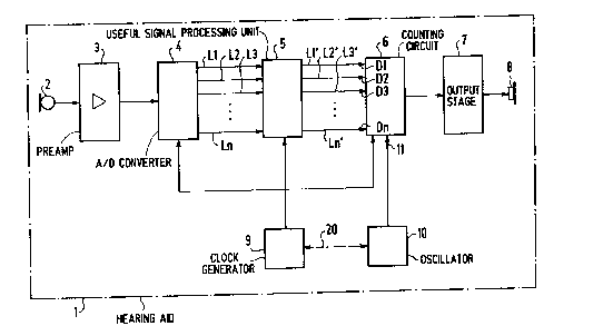
In Figure 1, a dot-dash line symbolically illustrates a hearing ald 1. The hearing
aid 1 comprises a microphone 2 as an input transducer that is connected to a processing
means for electrical useful signals. The processing means for useful signals in this
exemplary embodlment comprises a pre-amplifier 3, an analog-to-digitai converter 4, a
discrete-time useful signal processing unit 5, a counting clrcuit 6, and an output stage 7.
The output stage 7 is designed as a switching amplifier and is driven with a pulse-duration
modulated signal that can be taken from the counting circuit 6. The output stage 7
designed as a switching amplifier thus represents a circuit for a discrete-time signal
processing that is different from the discrete-time signal processing in the useful signal
processing unit 5. The output stage 7 is connected to an earphone 8 as an outputtransducer.
Preceding the output stage 7, the electrical useful signals supplied by the
microphone are sampled with a sampling frequency in the analog-to-digital converter 4
and are converted into data words. The data words, pref~rably as pulse-cod0-modulated
useful signals, are supplied via the lines L1 through Ln to the discrete-time useful signal
processing unit 5. Th0 processed data words are read into the counting circuit 6 via lines
2~99209
L1' through Ln' and via parallel inputs D1 through Dn. According to one version of the
invention, the counting circuit can also be serially loaded with the data words via a serial
input (not shown). The counting circuit 6, the useful signal processing unit 5, and the
analog-to-digital converter 4 in this exemplary embodiment are clocked with a sampling
frequency that can be taken from a clock generator 9. However, it is also possible to
design the counting circuit 6 such that drive with the sampling frequency can be foregone.
The counting circuit 6 receives counting pulses from an oscillator 10 that preferably
outputs square-wave pulses, receiving these via an input terminal 11. As a result of these
counting pulses, the counting circuit 6 is reset into an initial condition (low or high level)
after every data word read in via the parallel inputs D1 through Dn.
The chronological duration until the initial condition of the counting circuit 6occurs is mainly dependent on the binary value of the data word that is respectively read
in, and on the pulse repetition rate of the counting circuit. It was also recognized with the
inventlon that the chronological duration until the initial condition of the counting circuit 6
is reached fluctuates, dependent on the binary values of the data words. Since the binary
values of the data words are in turn dependent on the amplitude of the electrical useful
signals supplied by the microphone 2, the output signal of the counting circuit 6 must also
consequently be dependent on the amplitude of the analog, electrical useful signals
supplied by the microphone.
As a result of the successive input of data words into the counting circuit, forexample in the clock of the sampling frequency, the initial condition of the counting circuit
6 also changes in the clock of this sampling frequency. According to the invention, the
duration until the original initial condition of the counting circuit 6 is reached is a measure
for the amplitude of the analog, electrical useful signals supplied by the microphone 2.
The counting circuit 6, consequently, supplies a pulse-duration-modulated output signal
at its output side with which the output stage 7, which is designed as a switching amplifier,
can be driven.
2~9920~
In a development of the invention, the counting pulses supplied by the oscillator
10 have a repetition rate that is at least as high as the product of the sampling frequency
supplied by the clock generator 9 and the number ~2" raised by a maximally allowable bit r
plurality of data words. When "n" references the maximally allowable bit plurality of data
words and "fT" references the sampling frequency Uclock frequency", the repetition rate of
the counting pulses amounts to 2n fT.
The counting pulses can be derived from the sampling frequency by frequency
multiplication, or the sampling frequency can also be derived from the counting pulses by
frequency division. A synchronization between the sampling frequency of the clock and
the pulse repetition rate of the counting pulses can thus be achieved in a simple way.
This is indicated by the dashed double arrow 20 between the clock generator 9 and the
oscillator 10 in Figure 1. Consequently, only a shared oscillator is required. The circuit
expense and the space requirement are again reduced.
The counting circuit 6 shown as a block symbol in Figure 1 is shown in Figure
2 as a specific counting circuit 6 having the output stage 7 connecting thereto. The
counting circuit 6 contains a chain of flip-flop circuits that are designed as binary counters
F1 through Fn.
Each of the binary counters F1 through Fn has an input D that is connected to
respectively one of the inputs D1 through Dn of the counting circuit 6. Every data word
previously processed according to a first discrete-time method is supplied, for example
in parallel form, to the counting circuit via these inputs D1 through Dn. The individual bits
of each and every data word, therefore, place each of the binary counters F1 through Fn
into a switching condition corresponding to the respectively supplied bit. The input of the
data words can be control,ed (clocked) with the assistance of the sampling frequency via
an input 12 at the counting circuit 6. The number of binary counters F1 through Fn (at
least) corresponds to the plurality of the maximally allowable bit number of data words that
are supplied in parallel via the corresponding plurality of inputs D1 through Dn.
2~9~20~
Wi~h the binary counters F1 through Fn, the counting circuit 6 is designed as
a synchronously countlng counter circuit. The counting pulses suppliable via the input
11 of the counting circuit 6 are thereby simultaneously applied to all inputs C at all binary
counters F1 through Fn. So that all flip-flops of the binary counters do not change state
at every counting pulse, the binary counters F1 through Fn are designed as toggle flip-
flops that only change state when a control variable at their inputs Is T= 1, i.e. has a high
potential. A flip-flop in one of the binary counters F1 through Fn can consequently only
change state when all lower-value flip-flops are one, i.e. have already changed state. In
order to realize this, every output Q of a binary, less-significant counter F1 through F3 is
connected via an AND gate U1 through U3 to one of the respective inputs T of the binary
counters F2 through Fn. The input T of the binary counter F1 and the AND gates U1
through U3 are connected to a positive potential via a terminal 13, for example the
operating voltage of a hearing aid battery.
A further AND gate U4 is provided in the specific counting circuit 6 of Figure 2.
This AND gate U4 has its input side connected to all outputs Q of the binary counters F1
through Fn. Following therefrom is that the AND gate U4 only outputs an output signal
(high or low level) when all binary counters F1 through Fn have been reset into the initial
condition by the counting pulses supplied via the input 11 of the counting circuit 6.
As a consequence of the successive input of data words into the counting
circuit, the output signal output by the AND gate U4 is a pulse-duration-modulated signal.
This signal is supplied to the output stage 7, potentially via a driver 14, and is also
supplied thereto as a complementary signal via an inverter 15 because of the push-pull
design of the output stage 7.
The output stage 7 working as a switching amplifier comprises four MOSFET
transistors T1 through T4 working in switched mode in Figure 2. The transistors T1 and
T2 as well as the transistors T3 and T4 are respectively designed complementary relative
to one another. The output stage 7 is supplied with operating voltage via terminals 16 and
17. Due to the switched mode, either the transistors T1 and T4 or T3 and T2 are
20~9209
simultaneously transmissive. The time span within which the transistors are transmissive
is defined by the respective pulse duration of the individual pulses of the pulse-modulated
signal that is supplied to the switching amplifier from the counting citcuit 6 via inputs 18
and 19.
Given a change of the level in the pulse-duration-modulated signal, the
transistors that are transmlssive also change into the non-transmissive condition, and the
transistors that were previously non-transmissive thus become transmissive. As a result,
the earphone 8 arranged in the bridge arm of the output stage 7 is conseciuently switched
between the operating voltage (plus and minus pole) Iying at the terminals 16 and 17. As
a resuU of the low-pass effect of the earphone 8, the analog useful signal is filtered out of
the pulse-duration modulated signal and is made audible.
Although various minor changes and modifications might be proposed by those
skilled in the art, it will be understood that I wish to include within the claims of the patent
warranted hereon all such changes ani modifications as reasonably come within my
contribution to the art.