Language selection

Search

Patent 2099394 Summary

Third-party information liability

Some of the information on this Web page has been provided by external sources. The Government of Canada is not responsible for the accuracy, reliability or currency of the information supplied by external sources. Users wishing to rely upon this information should consult directly with the source of the information. Content provided by external sources is not subject to official languages, privacy and accessibility requirements.

Claims and Abstract availability

Any discrepancies in the text and image of the Claims and Abstract are due to differing posting times. Text of the Claims and Abstract are posted:

  • At the time the application is open to public inspection;
  • At the time of issue of the patent (grant).
(12) Patent: (11) CA 2099394
(54) English Title: DQPSK DELAY DETECTION CIRCUIT
(54) French Title: CIRCUIT DE DETECTION DE RETARDS DE MODULATION PAR DEPLACEMENT DE PHASE
Status: Expired and beyond the Period of Reversal
Bibliographic Data
(51) International Patent Classification (IPC):
  • H03D 05/00 (2006.01)
  • H04L 27/233 (2006.01)
  • H04L 27/38 (2006.01)
(72) Inventors :
  • NAKAYA, KAZUYOSHI (Japan)
(73) Owners :
  • MURATA MFG CO., LTD.
(71) Applicants :
  • MURATA MFG CO., LTD. (Japan)
(74) Agent: SMART & BIGGAR LP
(74) Associate agent:
(45) Issued: 1998-06-23
(22) Filed Date: 1993-06-30
(41) Open to Public Inspection: 1994-01-03
Examination requested: 1994-10-03
Availability of licence: N/A
Dedicated to the Public: N/A
(25) Language of filing: English

Patent Cooperation Treaty (PCT): No

(30) Application Priority Data:
Application No. Country/Territory Date
175 483/1992 (Japan) 1992-07-02

Abstracts

English Abstract


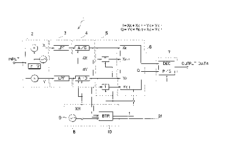
A DQPSK delay detection circuit includes a semi-synchronous detector
synchronously detecting an input signal to obtain two demodulated signals, a low-pass filter for
extracting a baseband signal from the demodulated signals, an A-D convertor sampling the
baseband signal by a clock signal with a frequency 32 times higher than a symbol rate frequency
and converting them to digital values with a predetermined number of quantization bits, a clock
pulse generator generating clock signals synchronized with the baseband signal and having a
frequency equal to and two times as high as the symbol rate frequency with a phase adjusted in
accordance with a change of an eye pattern of an output of the A-D convertor, a data delay unit
delaying the output of the A-D convertor by a time equivalent to one time slot according to a
clock signal synchronized with the baseband signal and having a frequency equal to the symbol
rate frequency, an operation unit generating signals I and Q from the output of the A-D
convertor and a one-time-slot-before output of the A-D convertor delayed by the data delay unit
according to a clock signal synchronized with the baseband signal and having a frequency equal
to the symbol rate frequency, and a judging unit demodulating an in-phase component signal and
orthogonal component signal from the signals I and Q and performing parallel-serial conversion
to output data.


French Abstract

L'invention est un circuit de détection de retards dans les signaux modulés par déplacement de phase différentiel en quadrature qui comprend un détecteur semi-synchrone servant à détecter en synchronisme les signaux d'entrée pour produire deux signaux démodulés, un filtre passe-bas servant à extraire un signal de bande de base de ces signaux démodulés, un convertisseur analogique-numérique qui échantillonne ce signal de bande de base à l'aide d'un signal d'horloge dont la fréquence est 32 fois plus élevée que la fréquence de transmission des symboles et qui le convertit en un signal numérique ayant un nombre prédéterminé de bits de quantification, un générateur de signaux d'horloge synchronisés avec le signal de bande de base ayant une fréquence double de la fréquence de transmission des symboles et une phase ajustée selon la modification du diagramme en oeil du signal de sortie du convertisseur analogique-numérique, une unité de retardement servant à retarder le signal de sortie du convertisseur analogique-numérique d'une durée correspondant à un créneau de temps d'après le signal d'horloge synchronisé au signal de bande de base dont la fréquence est égale à la fréquence de transmission des symboles, un générateur de signaux I et Q utilisant le signal de sortie du moment du convertisseur analogique-numérique et le signal de sortie de ce même convertisseur produit à un créneau de temps auparavant et retardé par l'unité de retardement selon le signal d'horloge synchronisé avec le signal de bande de base dont la fréquence est égale à la fréquence de transmission des symboles, et une unité d'évaluation qui démodule une composante en phase et une composante orthogonale des signaux I et Q et qui effectue une conversion parallèle-série pour produire les données de sortie.

Claims

Note: Claims are shown in the official language in which they were submitted.


- 12 -
THE EMBODIMENTS OF THE INVENTION IN WHICH AN EXCLUSIVE PROPERTY OR
PRIVILEGE IS CLAIMED ARE DEFINED AS FOLLOWS:
1. A DQPSK delay detection circuit comprising:
a semi-synchronous detector for synchronously detecting an input signal
to obtain two demodulated signals,
a low-pass filter for extracting a baseband signal from each of the two
demodulated signals,
an A-D converter for sampling the two baseband signals by a clock signal
with a frequency sufficiently higher than a symbol rate frequency, in order to obtain
high fidelity of signal demodulation, and converting the two baseband signals from
analog to digital values with a predetermined number of quantization bits to produce an
output,
a clock pulse generator for generating second and third clock signals
synchronized with the two baseband signals, said second clock signal having a
frequency equal to the symbol rate frequency and said third clock signal having a
frequency two times as high as the symbol rate frequency, with a phase adjusted in
accordance with a change of an eye pattern of the output of the A-D convertor,

-13 -
a data delay unit for delaying the output of the A-D convertor by a time
equivalent to one time slot according to the second clock signal,
an operating unit for generating signals I and Q from the output of the A-D
convertor and a one-time-slot-before output of the A-D convertor delayed by the data
delay unit according to the second clock signal,
and
a judging unit for demodulating an in-phase component signal and
orthogonal component signal from the signals I and Q and performing parallel-serial
conversion to output data.
2. A DQPSK delay detection circuit according to claim 1, wherein said two
demodulated signals from said semi-synchronous detector include an in-phase detection
signal and an orthogonal detection signal.
3. A DQPSK delay detection circuit according to claim 1, wherein said A-D
converter samples the two baseband signals by a clock signal with a frequency 32
times higher than the symbol rate frequency.

- 14 -
4. A DQPSK delay detection circuit according to claim 1, wherein said A-D
convertor converts the two baseband signals from analog to digital values with six
quantization bits.
5. A DQPSK delay detection circuit according to claim 1, wherein the clock
pulse generator includes a clock signal generation circuit which produces said first clock
signal with the frequency sufficiently higher than the symbol rate frequency, and a bit
timing recovery circuit connected with the clock pulse generator and the A-D convertor
and which produces the second clock signal having the frequency equal to and the third
clock signal having the frequency two times as high as the symbol rate frequency with
the phase adjusted in accordance with the change of the eye pattern of the output of
the A-D convertor.

- 9 -
6. A DQPSK delay detection circuit according to claim 5, wherein said bit timing
recovery circuit includes:
an opening detection unit connected with the A-D convertor and which
detects a timing when an opening of the eye pattern is at a maximum and outputs
an opening timing signal,
a window setting unit connected with the opening detection unit for
outputting a window signal with a predetermining time length by using the
opening timing signal as a trigger,
a zero cross detection unit connected with the A-D convertor and which
detects a zero cross point of the eye pattern and outputs a zero-cross-point timing
signal,
an AND gate connected with the window setting unit and the zero cross
detection unit, and which outputs the zero-cross-point timing signal when the
window signal is input thereto,
a DPLL unit connected with an output of the AND gate and which
generates the clock signal synchronized with the baseband signal and having a
frequency equal to the symbol rate frequency, and
a frequency doubling circuit connected with an output of the DPLL unit
and which generates the clock signal synchronized with the baseband signal and
having a frequency two times as high as the symbol rate frequency.

Description

Note: Descriptions are shown in the official language in which they were submitted.


TITLE OF THE INVEN~ION
3 9 ~
DQPSK DELAY DETECTION CIRCUIT
BACKGROUND OF THE INVENTION
F~eld of the Invention
The present invention relates to a DQPSK (Differential Quaternary Phase Shift
Keying) delay detection circuit and in particular to a DQPSK delay detection circuit for
m~teri~li7.ing a low power consumption and minimi7ing the circuit size.
D~.;~lion of the Prior Art
FIG. 4 is a block diagram showing the structure of the DQPSK delay detection
circuit lepolled in "Proce~ling of The 1990 IEICE Fall Conference; B-300 Coneti~ltion and
characteristics of p/4 shift QPSK b~eeb~nd delay detector".
This DQPSK delay det~tion circuit 51 comprises a semi-synchronous detector 2,
low-pass filter 3, A-D convertor 4, data delay unit 55, operation unit 56, judging unit 7, and
clock pulse generator 58.
The data delay unit 55 has a shift register T'. The clock pulse generator 58 is
provided with a clock signal generation circuit 9 and BTR (Bit Timing Recovery) 60.
1~ - 1

2~9939~
The clock signal generation circuit 9 of the clock pulse
generator 58 supplies a 32f clock signal, a signal with a frequency
32 times as high as the symbol rate frequency f, to the A-D convertor
4, data delay unit 55, and operation unit 56. The BTR 60 of the clock
pulse generator 58 supplies a 2f clock signal, a signal with a
frequency two times as high as the symbol rate frequency f, to the
judging unit 7.
In the above mentioned DQPS~ delay detection circuit 51, semi-
synchronous detector 2 synchronously detects an input signal, the
obtained in-phase detection output ~ and orthogonal detection output
Y is passed through the low-pass filter 3, the A-D convertor 4 samples
the outputs X and Y at a frequency 32 times as high as the symbol rate
frequency f, and performs an analog to digital conversion with six
quantization bits. The shift register T' of the data delay unit 55
delays the output of the A-D convertor 4 by a time equivalent to the
one time slot.
In the next step, the present output of the A-D convertor 4 and
the one-time-slot-before output, delayed by the data delay unit 55,
of the same is computed to obtain orthogonal signals I and Q
containing a code bit information. Further, BTR (Bit Timing
Recovery) 60 of the clock pulse generator 58, regenerates a 2f clock
signal on the basis of the timing of the code bit of the signal Q
outputted from the operation unit 56, the judging unit 7 selects a

~ ~ ~ Q ~ g 4
~,.........
point with the largest eye apellur~ among 32 sample points in one time slot on the basis of the
regenerated 2f clock signal, in-phase signal and orthogonal signal modulations and parallel-serial
conversions are pelrol,lled before ou4,.1lling the data.
In the above explained conv~n~ion~1 DQPSK delay detection circuit 51, each of
the units~-D convertor 4, data delay unit 55, and operation unit 56) on the way to the operation
unit 56 ~lrOll,ls high-speed processing at the 32f frequency, which is 32 times as high as the
symbol rate frequency f, till the BTR 60 of the clock pulse generator 58 generates a 2f clock
signal on the basis of the timing of the code bit of the signal Q.
There occurs a drawback that the power consumption increases because the high-
speed proc~ssing is pelrornled at a frequency 32 times as high as the symbol rate frequency f.
~ ss~-ming the number of qll~nti7~tion bits in the A-D convertor 4 as m and the
ratio of the sampling frequency to the symbol rate frequency (=sampling frequency/symbol rate
frequency) in the shift register T' of the data delay unit 55 as n, 2mn flip flops are required for
the shift register T' of the data delay part 55 in general. Re~llse the above embodiment
according to the prior art required "2 x 6 x 32" flip flops, a problem occurs that a large shift
register T' becomes nects~dly and thereby a decrease of circuit size is difficult.
",

2~3~ 4
SUMMARY OF THE ~VENTION
It is an object of the present invention to provide a DQPSK delay detection circuit
for mqteriqli7ing a low power coneumption and minimi7ing the circuit size.
The DQPSK delay detection circuit of the present invention is chqrvq~tPri7~d by
comprising a semi-synchronous detector for synchronously detecting an input signal to obtain two
demod~ t~d signals such as an in-phase det~ction signal and orthogonal detection signal, a low-
pass filter for extracting a b~seb~nd signal from these two demodulated signals, an A-D
convertor for sampling the bq.~eb~nd signal by a clock signal with a frequency sufficiently higher
than the symbol rate frequency and converting them from .nalog to digital values with a
predetermined number of quantization bits, a clock pulse genel~tor for generating clock pulse
signals synchronized with the b~bqn d signal and having a frequency equal to and a frequency
two times as high as the symbol rate frequency respectively according to the change of an eye
pattern of the output of the A-D convertor, a data delay unit for delaying the output of the A-D
convertor by the time equivalent to one time slot according to a clock pulse signal synchroni_ed
with the b-q-~bq-nd signal and having a frequency equal

2099~
to the symbol rate frequency, an operation unit for generating
signals I and Qfrom the present output of the A-D convertor and the
one-time-slot-beforeoutputoftheA-Dconvertordelayedbythedata
delay circuit according to a clock signal synchronized with the
baseband signal and having a frequency equal to the symbol rate
frequency,andajudgingunitfordemodulating anin-phasecomponent
signal and orthogonal component signal from the signals I and Q
according to a clock pulse signal synchronized with the baseband
signal and having a frequency two times as high as the symbol rate
frequencyandperformingparallel-serialconversiontooutputdata.
The DQPS~ delay detection circuit of the present invention
obtains abasebandsignalfromaninputsignalby asemi-synchronous
detector and low-pass filter and converts the baseband signal from
analog to digital values by an A-D convertor. Then, the circuit
computes the present output of the A-D convertor and the
one-time-slot-before outputof the A-D convertor delayed by a delay
unitusinganoperationunittoobtainsignalsI andQ. Moreover, the
circuit obtains data from the signals I and Q using the judging unit
to output the data.
In this case, the clock pulse signal supplied to the delay unit
andtheoperationunitisgeneratedaccordingtothechangeoftheeye
pattern of the output of the A-D convertor, which is synchronized
with the baseband signal and has the symbol rate frequency.

3 9 4
As described above, because the clock pulse signal synchronized with the baseband
signal and having the symbol rate frequency is generated to operate the delay unit and operation
unit, the power consumption can be decreased co"lpaled with the existing conventional circuit
which is operated at a high speed. Moreover, the size of the delay unit and circuit can be
decreased.
Brief Desc~ption Of The Drawings
FIG. 1 is a block diagram of the DQPSK delay detection circuit which is an
embodiment of the present invention;
FIG.2is a block diagram of a clock pulse generator;
FIG. 3 is an illustration for explaining an eye pattern of the output of an A-D
convertor; and
FIG.4is a block diagram of a conventional DQPSK delay detection circuit.
Spe~ Description of The Embodiment
The present invention is more precisely described below according to an
embodiment shown in the drawings. However, the present invention is not restricted to the
embo lim~nt
FIG.lis a block diagram of the constitution of the DQPSK delay

3 ~ ~
~7...
detection circuit which is an embodiment of the present invention.
The DQPSK delay ~e~ti- n circuit 1 comprises a semi-synchronous detector 2,
low-pass filter 3, A-D convertor 4, data delay unit 5, operation unit 6, judging unit 7, and clock
pulse generator 8.
The data delay part 5 has a shift register T.
The clock pulse generator 8 is provided with a clock signal generation circuit 9
and BTR 10.
A 32f clock signal with a frequency 32 times as high as the symbol rate frequency
f is supplied to the A-D convertor 4 from the clock signal generation circuit 9 of the clock pulse
generator 8.
A clock signal f with a symbol rate frequency f is supplied to the data delay unit
5 and the operation unit 6 from the BTR 10 of clock pulse geneMtor 8.
Moreover, a 2f clock signal with a frequency two times as high as the symbol rate
frequency f is supplied to the judging unit 7 from the BTR 10 of the clock pulse generator 8.
As shown in FIG. 2, the BTR 10 comprises an opening detection unit lOa,
window setting unit lOb, zero cross detection unit lOc, AND gate unit lOd, DPLL unit lOe, and
frequency doubling circuit lOf.

20~93~
TheoperationsoftheDQPS~delaydetectioncircuitaredescribed
in detail in the following.
The DQPS~ delay detection circuit 1 synchronously detects an
input signal using the semi-synchronous detector 2 and passes the
obtainedin-phasedetectionoutputXandorthogonaldetectionoutput
Y through the low-pass filter 3 to obtain a baseband signal. This
DQPS~ delay detection circuit 1 then samples the baseband signal
usingtheA-Dconvertor4atafrequency32timesashighasthesymbol
rate frequency f to convert the signal from analog to digital values
with si~ quantization bits.
A-D converted digital data values Xk and Yk are inputted to the
data delay unit 5 and the BTR 10 of the clock pulse generator part 8.
The digital datavaluesXk andYkinputtedto the data delayunit
5are directlYoutputted to theoperationunit6and alsoinputted to
shift registers T and T. The shift registers T and T output digital
datavaluesXk-l andYk-l whicharedelayedbythe time equivalentto
one time slot to the values inputted to the operation unit 6.
The digital data values Xk and Yk inputted to the BTR 10 of the
clock pulse generator 8 are supplied to the opening detection unit
lOa and zero cross detection unit lOc.
FromthedigitaldatavaluesXkandYktheopeningdetectionunit

2~33~
lOa detects the timing (point A in Fig. 3) when the opening of an eye
patternismaximumandoutputsanopeningtimingsignaltothewindow
setting unit lOb.
The window setting unit lOb starts a timer using the opening
timing signal as a trigger. The timeroutputs a window signal with a
predetermined time length (the width of the window shown in Fig. 3)
to the AND gate unit lOd.
From the digital data values ~k and Yk the zero cross detection
unit lOc detects a zero cross point (point B in Fig. 3) of the eye
pattern andoutputs azero-cross-pointtimingsignal tothe AND gate
unit lOd.
The AND gate unit lOd passes further the inputted zero-cross-
point signal while the window signal is inputted.
The DPLL unit lOe generates a clock signal f from a 32f clock
signal. When the zero-cross-poin* timing signal is inputted to the
DPLL unit lOe, the DPLL unit lOe judges the delay and or the lead of
thephaseoftheclocksignalftoadjustthe timing. As aresult, the
clock signal f synchronizes with the baseband signal and becomes a
clock signal with the symbol rate frequency f.
Frequency doubling circuit lOf generates a clock signal 2f
synchronizing with the baseband signal and having a frequency two

2~9'~9~
times as high as the symbol rate frequency f from the clock signal f.
As described above, when assumed the number of quantizationbits
in the A-D conversion part 4 as m and the ratio of the sampling
frequency to the symbol rate frequency (= sampling frequency/symbol
rate frequency) in the shift register T of the data delay part 5 as n,
2mn flip flops are required for the shift register T of the data delay
unit 5. For this embodiment, however, the shift registerT requires
only "2 x 6 x 1" flip flops because the clock signal f synchronized
with the baseband signal and having the symbol rate frequency f is
supplied to the data delay unit 5. Moreover, the power consumption
decreases.
The operationunit 6 performs apredetermined operationwith the
digltal data values Xk and Yk and the one-time-slot-before digital
data values Xk-l and Yk-l to demodulate orthogonal signals I and Q.
In this case, the power consumption decreases because the clock
signal f synchronized with the baseband signal and having the symbol
rate frequency f is supplied to the operation unit 6.
The DQPSE delay detection circuit of the present invention makes
it possible to control power consumption because the delay part and
operation part are operated by a clock signal synchronized with the
baseband signal and having the symbol rate frequency f. Moreover,
the circuit can be simplified and decreased in size because the

20993~
. .
number of shift registers in the delay part can be decreased.

Representative Drawing
A single figure which represents the drawing illustrating the invention.
Administrative Status

2024-08-01:As part of the Next Generation Patents (NGP) transition, the Canadian Patents Database (CPD) now contains a more detailed Event History, which replicates the Event Log of our new back-office solution.

Please note that "Inactive:" events refers to events no longer in use in our new back-office solution.

For a clearer understanding of the status of the application/patent presented on this page, the site Disclaimer , as well as the definitions for Patent , Event History , Maintenance Fee  and Payment History  should be consulted.

Event History

Description Date
Time Limit for Reversal Expired 2012-07-03
Letter Sent 2011-06-30
Inactive: IPC from MCD 2006-03-11
Grant by Issuance 1998-06-23
Pre-grant 1998-03-12
Inactive: Final fee received 1998-03-12
Notice of Allowance is Issued 1997-12-22
Letter Sent 1997-12-22
Notice of Allowance is Issued 1997-12-22
Inactive: Status info is complete as of Log entry date 1997-12-17
Inactive: Application prosecuted on TS as of Log entry date 1997-12-17
Inactive: IPC removed 1997-12-01
Inactive: IPC assigned 1997-12-01
Inactive: IPC removed 1997-12-01
Inactive: First IPC assigned 1997-12-01
Inactive: IPC assigned 1997-12-01
Inactive: Approved for allowance (AFA) 1997-11-26
All Requirements for Examination Determined Compliant 1994-10-03
Request for Examination Requirements Determined Compliant 1994-10-03
Application Published (Open to Public Inspection) 1994-01-03

Abandonment History

There is no abandonment history.

Maintenance Fee

The last payment was received on 1997-06-16

Note : If the full payment has not been received on or before the date indicated, a further fee may be required which may be one of the following

  • the reinstatement fee;
  • the late payment fee; or
  • additional fee to reverse deemed expiry.

Patent fees are adjusted on the 1st of January every year. The amounts above are the current amounts if received by December 31 of the current year.
Please refer to the CIPO Patent Fees web page to see all current fee amounts.

Fee History

Fee Type Anniversary Year Due Date Paid Date
MF (application, 4th anniv.) - standard 04 1997-06-30 1997-06-16
Final fee - standard 1998-03-12
MF (patent, 5th anniv.) - standard 1998-06-30 1998-06-23
MF (patent, 6th anniv.) - standard 1999-06-30 1999-05-18
MF (patent, 7th anniv.) - standard 2000-06-30 2000-05-18
MF (patent, 8th anniv.) - standard 2001-07-02 2001-05-16
MF (patent, 9th anniv.) - standard 2002-07-01 2002-05-16
MF (patent, 10th anniv.) - standard 2003-06-30 2003-05-20
MF (patent, 11th anniv.) - standard 2004-06-30 2004-05-17
MF (patent, 12th anniv.) - standard 2005-06-30 2005-05-09
MF (patent, 13th anniv.) - standard 2006-06-30 2006-05-05
MF (patent, 14th anniv.) - standard 2007-07-02 2007-05-07
MF (patent, 15th anniv.) - standard 2008-06-30 2008-05-12
MF (patent, 16th anniv.) - standard 2009-06-30 2009-05-14
MF (patent, 17th anniv.) - standard 2010-06-30 2010-05-11
Owners on Record

Note: Records showing the ownership history in alphabetical order.

Current Owners on Record
MURATA MFG CO., LTD.
Past Owners on Record
KAZUYOSHI NAKAYA
Past Owners that do not appear in the "Owners on Record" listing will appear in other documentation within the application.
Documents

To view selected files, please enter reCAPTCHA code :


To view images, click a link in the Document Description column. To download the documents, select one or more checkboxes in the first column and then click the "Download Selected in PDF format (Zip Archive)" or the "Download Selected as Single PDF" button.

List of published and non-published patent-specific documents on the CPD .

If you have any difficulty accessing content, you can call the Client Service Centre at 1-866-997-1936 or send them an e-mail at CIPO Client Service Centre.


Document
Description 
Date
(yyyy-mm-dd) 
Number of pages   Size of Image (KB) 
Abstract 1994-03-12 1 11
Claims 1994-03-12 1 37
Drawings 1994-03-12 4 90
Description 1994-03-12 11 294
Abstract 1997-11-12 1 36
Description 1997-11-12 11 326
Claims 1997-11-12 4 98
Drawings 1997-11-12 4 89
Representative drawing 1998-06-21 1 9
Commissioner's Notice - Application Found Allowable 1997-12-21 1 165
Maintenance Fee Notice 2011-08-10 1 170
Correspondence 1998-03-11 1 43
Fees 1997-06-13 1 37
Fees 1998-06-22 1 50
Fees 1996-06-24 1 41
Fees 1995-04-24 1 46
PCT Correspondence 1995-09-18 1 31
Prosecution correspondence 1995-04-18 13 399
Prosecution correspondence 1994-10-02 1 46
Prosecution correspondence 1997-10-05 3 42
Examiner Requisition 1997-04-03 2 94