Note: Descriptions are shown in the official language in which they were submitted.
2~9~
SPECIFICATION
Title of the Invention
SUPERCONDUCTINa DEYICE HAVING A
S SUPERCONDUC'rlNG CHANNEL FORMED OF OXIDE
SUPERCONl:3UCTOR MATERIAL AND METHOD FOR
MANVFACTURING THE SAME
13ackground of the Invention
Field of the invention
The present invention relates to a superconducting device and a
me~hod for manufacturing ~he same, and more specifically to a
superconducting device having an extremely ~hin superconduc~ing channel
formed of oxide superconductor material, and a method ~or
manufacturing the same.
Description of related art
I)evices which utilize supe~conducting phenomena operate rapidly
with low power consumption so that they have higher performance th~n
conventional semiconductor d~vices. Particularly, ~y using an oxide
superconducting material which has been recently advanced in study, it is
possible to produce a superconducting device which operates at relatively
high temperature.
Josephson d~vice is one of well known superconducting deYices.
2 5 However, since Josephson device is a two-terminal device, a lagic ga~ewhich utilizes Josephson devices ~ecomes compiicated configura~ion.
Therefore, three-terrninal superconducdng devices are more practic~
209~r~0
Typical three-terminal superconducting devices include two types of
super-FET (field effect transistor). The first type of the super-FET
includes a semiconductor channel, and a superconductor source electrode
and a superconductor drain electrode which are formed closely to each
S other on both side of the sem;conductor channe~. A portion of the
semiconductor layer between the superconductor source electrode and ~e
superconductor drain electrode has a greatly recessed or undercut rear
sur~ace so as to have a r~duced thickness. In addition, a gate electrode is
formed through a gate insulating layer on the portion of lhe recessed or
10 undercut rear surface of the semiconductor layer between the
superconductor source electrode and the superconductor drain electrode.
A superconducting current flows through the semiconductor lay~r
(channel) between the superconductor source electrode and the
superconductor drain eiectrode due to the superconducting proximity
1 S effect, and is controlled by an applied gate voltage. This type of the
super-FET operates at a hi~her speed with a lowe~ power consumption.
The second type of the super-FET includes a channel of a
superconductor formed between a source electrode and a drain electrode,
so that a current flowing through the superconducting channel is
2 0 controlled by a voltage applied to a gate formed above the
superconducting channel.
Both of the super-FETs mentioned above are voltage controlled
devices which are capable of isolating output signals from input ones and
of haYing a well defined gain.
However, sinee the first type of the super FET uti~izes the
superconducting proximity effect, ~he superconductor source electrode
and the superconduetor drain electrode have to be positioned within a
2Q99~0
distance of a few times the coherence length of the superconductor
materials of the superconductor source electrode and the superconductor
drain electrode. In particular, since an oxide superconductor has a short
coherence length, a distance between the superconductor source electrode
5 and the superconductor drain electrode has to be made less than about a
few ten nanometers, if the superconductor source electrode and the
superconductor drain e}ectrode are formed of the oxide superconduc~or
material. However, it is very difficult to conducl a fine processing such
as a fine pa~tern etching, so as to satisfy the very short separation dis~ance
10 mentioned above.
On the other hand, the super-PET having the superconducting
channel has a large current capability, and the fine processing which is
required to product the first type of the super-F~T is not needed ~o
product this type of super^FET.
ln order to obtain a complete ON/OFF operation by a signal voltage
of several volts applied to the gate electrode, both of the superconducting
channel and the gate insulating layer should have an extremeiy thin
thickness. For example, ~he superconduct1ng channel ~ormed of an oxide
superconductor material should have a thickness of less than five
20 nanometers and the gate insulating layer should have a thickness more
than ten nanometers which is ~ufficien~ to prevent a tunnel current.
The super-FEll has a superconducting source region and a
superconducting drain region which have a sufficient thickness ~or
forming contacts on them, for example more than 200 nanometers. Since,
2 5 the relatively thick superconducting source region and the
superconducting drain region are arranged at the both ends of the
extremely thin superconducting channel, the super FET may not have a
2~9~
planar upper surface. In this case, resolution of photolithography is
spoiled so that the super-FET can no~ be manufactured so as to have a
t~quired ~Ine structure. The amount of the in~egration of the super-FET
is also limited by the resolution of photolithography .
In addi~ion, in a prior art, in order to increase the superconducting
current through interfaces between the superconducting channel and the
superconducting source region and between ~he superconducting channel
and the superconducting drain region, the superconducting source region
and the superconducting drain region may be processed by etching so that
they are smoothly connected to the superconducting channel.
However, the oxide superconductor thin films which consti~uted of
the superconducting source region and the superconducting drain region
are degraded during the etching so that the superconducting
characteristics is affected. In addition, the etched surface of the oxide
superconductor thin film is roughened. Therefore, if an oxide
superconductor thin fi:lm which is cons~ituted of the extrcmely thin
superconducting channel is formed on the rough sut~ace, its clystallinity
and the superconduc~ing properties are also affected. Addit;onally, an
undesirable Josephson junction or resistance is generated at these
2 0 inter~aces.
By this, the super-FET manufactured by the above conventional
process does not h~ve an enough performance.
Summary of thc Invention
2 5 Accordingly, it is an object of the present invention to provide an
FET type sa~perconducting device having a superconducting channel
4 ~
~99~
constituted of an extremely thin oxide superconductor film, which h~Ye
overcome the above mentioned defects of the conventional ones.
Another object of the present invention is to provide a method for
manufacturing an FET type superconducting device which have overcome
5 the above mentioned defects of the conventional ones.
The above and other objects of the present invention are achieved in
accordance with the present invention by a superconducting device
comprising a substrate h~ving a principal sur~ace, a non-superconducting
oxide layer having a similar crys~al structure to that of an oxide
1 û superconductor formed on the principal surface, which can compensate~
the lattice mismatch between the substrate and the oxide superconductor, a
superconductin~ source region and a superconducting drain region
formed of c-axis orien~ed oxid~ superconductor thin films on the
non^superconducting oxide layer, an insulating region formed of a doped
15 oxide superconductor on the non-superconducting oxide layer separating
the superconducting source region and the superconducting drain region9
an extremely thin superconducting channel on the insulating region,
forrned of a c-axis oriented oxide superconductor th1n film which is
prolonged to the superconducting sollrce region and the superconducting
20 ~rain regjon, which electrically connects the superconducting source
re8ion to the superconducting drain reginn, so that superconducting
~urren~ can flow through the superconducting channel between the
superconduc~ing source region and the superconducting drain region, and
a gate electrode through a gate insu]ating layer on the superconducting
25 channel for controlling the supereonducting current flowing through the
superconducting channel ~y a signal voltage applied to the gate electrode,
in which the sup~rcondllcting sour~e region, the sllperconducting drain
2 0 ~-3 ~
region and thç insulating region have the same thickness so that the
extremely thin oxide superconductor thin film which constitutes the
superconducting channel is forrned flatwise.
In ~he superconducting dcYice in accordance with the present
S invention, the superconducting channel, ~e part of the superconducting
source region and the part of the superconducting drain region are
fonned of one c-axis oriented oxide superconductor thin film, therefore
there is no undesirable resistance nor undesirable Josephson junction
between the superconducting channel and the superconducting soLIrce
O region and between the superconducting channel and the superconducting
drain region.
The insulating regiorl, the superconducting source repion and the
superconducting drain region of the super-FET in accordance with the
present invention h~ve the same thickness. By this, the extremely thin
15 oxide supercnnductor thin film which constitutes the superconducting
channel can be formed flatwise. This improves not only the
characteristics of the superconducting channel but also resolution of
photolithography so that the gate insulat}ng layer, the gate electrode, the
source electrode and the drain electrode can be accurately ~onned on the
20 extremely thin oxide superconductor thin film through photolithography
process~ ~n particular, the gate insulating layer and the gate electrode
~,hould be accurately formed in size and position f~r an excellent
per~rmance of tlle device~ The above structures of the 1nsulating region,
dle sup~rconducting source region and the superconducting drain region
25 insure the fine photolithography which is needed to ~orm the gate
insula~ing layer and ~he gate electrode accurately.
209~0
In one preferable embodiment of the present invention, ~he
interfaces between the insulating region and the superconducting sollrce
region and between the insulating region and the superconduc~ing drain
region inclines so dlat the insulating region has a narrowing spacing at ~h~
5 top.
The inclined sidcs of the insulating region improve the conductance
of superconducting current flowing from the superconducting source
region into the extremely thin superconducting channel ~nd flowing from
the extremely thin superconducting channel to the superconducting drain
I O region. By this, the current capability o~ the super-FET can be improved.
For this pulpose, the tilt angles of ~he sides of the insulating region to the
principal surface of the oxide layer are preferably smaller than 4~. If
the tilt angles are larger than 45, the superconducting current can not
flow so efficient~y.
In ~he superconducting device in accordance with the present
invention, the non-superconducting oxide layer pre~erably h~s a similar
crysta~ structure to that of a c-axis oriented oxide superconductor thin
film. In this c2se, the insulating region, the supercondueting source
region and the swperconducting drain region, and alsv the
20 superconducting channel of a c-axis oriented oxide or a c-axis oriented
oxide superconductor thin film can be easily formed on the oxide layer.
Prefer~bly, the above non-swpercolldllctin~ nxide laye~ ia folmed of
a PrlBa2Cu307 y oxide. A c-axis oriented PslBa2(: u3O7.y thill film has
almost the same crys~a~ :lattice strueturg as that of a c-axis ori~nted oxide
2 5 superconductor thin film. It compensates the la~tice mismatch between the
substrate and the oxide superconductor, therefore, the crystalline
incompleteness of the c-axis oriented oxide superconduct~r is g~eatly
7 ii
ii
2 0 ~ nf~ 6 !1 (3
improved at its bottom located on the PrlBa2Cu30~ y thin film. ~n
addition, the effecl of diffusion of the constituent elfemen~s of
PrlBa2Cu307.y into the oxide superconductor thin film is negligible and i~
also prevents the diffusion frofm substrate. Thus, the oxide
superconductor thin film depcfsited on the PrlBa2Cu307.y thin film has a
high quality.
In a preferred embodiment, the oxide superconductor is formed of
high-TC (high critical tf~mperature) oxide superconductor5 particularly~
formed of a high-TC copper-oxide type compound oxide superconductor
for example a Y-Ba-Cu-O comp~und oxide superconductor material, ~
13i-Sr-Ca-Cu-O cofmpound oxide superconductor material, and a
Tl-Ba-Ca-fCu-fO compound oxide superconductor mate~ial. ¦~
In addition, ~he substrate cfan be formed of an insulating substrate,
preferably an oxide single cryst~lline substrate such as M~O, SrTiO3, f
YSZ, etc. These substrate materials are very effective in fonning or
growing a crystalline film having a well defined crystalline orientation.
However, in one preferred embodiment, ~he super-FET can ~ ¦
formed on a substrate of a conductivc material, if the above oxide ]ayer is
deposited tl~,ereon. If the substrate is formed of a conductive material~ a
2 0 substrate potential can be appiied to the super-FET of this structure. By
this, the substrate to wl~ich a potential is applied can shield
~lectro-magnetic field around the super FET, so that the superconducting
channel of the super-FET is not affected by the other devices located ne~r
the super-FET. In addit~on, the electric lines of force generated by ~e
2~ ~pplied gate voltage is terminated at ehe subsffffrate, so that ~his type of
super-FET is hardly affected by ~ bfack gate feffee~ caused by the elect~ic
1,
f,
2~9~h.~ O
field around ~he super-FET. Therefore, ~e operation of the super-FET
is stabilized and reliable.
Additionally, since the substrate potential is maintained, leakage of
superconducting current is prevented when a voltage is applied to the gate
5 electrode so as to shut the channel completely. The substrate also
functions as a magnetiG shield of a back plane so that the supercondu~ting
port;ons of the super-FET is not affected by magnetic field around the
super-FET.
By applying a signal voltage to the substrate corresponding to the
O signal voltage applied to the gate clectrode, it is also possible to fonn a
double sided and/or dual gate structure. By this, modulation of
superconducting current flowing through the superconducting channel
becornes easier.
According to ano~her aspect of the present invention, there is
15 provided a method of manufacturing a superconducting device comprisitlg
~he steps of depositing on a principal surface of a sub~ra~e a
non-superconducting oxide layer having a similar crystal structure to that
of a c-axis oriented uxide supere~nductor thin film, depositing a first
c-axis oriented oxide superconductor thin film having a sufficient
2 0 ~ickness ~or forming a contact on it on the non-superconducting oxide
layer, impla~ting an impurity ion beam to a center portion of the fhst
oxide superconductor thin film so ~at a insulating region is ~ormed at ~ae
center portion of the first oxide superconductor thin film, which divides
the first oxide superconductor ~hin filTn into a superconduç~ing source
2 5 region and a superconducting drain region, depositing an extreme]y thin
second c-axis oriented oxide supercond~lctor thin film on the first oxide
superconductor thin ~llm so as to form a superconducting channel on the
2~3~9~4~3
insulating region, depositing an insulating layer on the second c-axis
oriented oxide superconductor thin ~llm so as to form a gate insulating
layer on ~he superconducting channel, and forrning a gate electrode on dle
gate insulating layer.
S In ~e above me~od in accordance with the present invention, no
etching process is necessary for processing an oxide superconductor thin
film. Therefore, oxide superconductor thln films of the super-FET are
not degraded, so that ~he oxide superconductor thin films ha-re good
superconducting characteristics.
In one preferred embodiment, the ion beam is implanted with the
incident angle relative to the oxide superconductor thin ~ilm jn an rallge
larger than 45 so that the largest incident angle of the ion beam to the
nsrma~ line of the oxide superconductor thin film is not smaller than 45
and the smallest incident angle is more less than -45. It is not necessary
that the ion beam is irradiated symmetrically to the nolmal line of the
supercondllctor thin film.
According to still another aspect of the present invention, th~re is
provided a method of manu~cturing a superconducting device,
comp~ising the s~eps of depositin~ on a principal surface of a subst~ate a
2 0 non-superconducting oxide layer having a similar crystal structure to that
~f a c-axis orien~ed oxide superconductor thin film, depositing a c-axis
ori~nted oxide superconductor thin film h~ving a thickness of several
parts of a superconducting source region and a superconducting ~r~in
region on the non-superconductillg oxide layer, implanting an impllrity
2 5 ion beam to a center portion of the oxide superconductor thin film so that
an insulating region is formed at the center portion of the oxide
superconductor thin film~ which divides the oxide superconductolt thin
1.
209~6 -1~
film into two par~, depositing another c-axis oriented oxid~
superconductor thin ~llm of substan~ially the same thickness on ~he oxide
superconductor thin film having ~he insulating region, implanting an
impurity ion beam to a center portion of the upper oxide superconducto~
thin film so that a narrower insulating region is forrned at the center
por~ion of the oxide superconductor thin film than tha~ of the previously
deposited oxide superconductor thin film, which divides the oxide
superconductor thin film into two part, repeating the processes of
depositing an oxide superconduc~or thin film of substantially the sanne
10 thickness and of forming a narrow~r insulating region than tha~ of d~e
lower oxide superconductor thin film by implanting the impurity ion
beam so that a superconduc~ing source region and a superconducting drain
region having a sufficienl thi~kness for forming a contacts on ~hcm
separ~ted by an insulating region having a narrow spacing at the top,
15 depositing an extremely thin c-axis oriented oxide superconductor thin
film on ~he superconducting source region, the superconducting drain
region and the insulating region so as to form a superconducting channel
on the insulating region, depositing an insulating layer on the extr~mely
thin c-a~is oriented nxide superconductor thin film so as to fo~m a g~ste
20 insulatan~ layer on the superconducting channel, and fo~ming a gate
electrode on the gate insul~ting layer.
The above and other objectsl ~eatures and advantages of ~he pr~sent
invention will be apparent from the following description of prefer~d
~mbodiments of the invention with reIerence to the acCompanyiDg
2 5 drawislgs.
~.
~a~6~l~
Brief Description of lhe Drawings
Figures lA to lH a~ diagrammatic sectional views ~or illustrating
an embodiment of Ihe process in accordance with the present invention
for manufactunng the super-FET;
Figure 2 is a diagrammatic sectional view of one variation of the
super-~ET in accordance with the present invention;
Figures 3A to 3F are diagrarnmatic sectional views for illustrating
featured steps of a second embodiment of the process in accordance with
the present invention for manufacturing the super-FET;
Figure 4 is a diagrammatic sectional view of sti31 an~ther
embodiment of ~ super-FET in acco~dance with the present invention;
~d
Figure 5 is a plane view for illustrating the configuration fsr
eva)uating the back gate effect on the superconducting channel of ~e
1 5 super-FET.
Description of the Preferred embodiments
Embodiment 1
Referring to Figures lA t() 1H, the process in accordancc wiib the
2 0 present invent;on for manufacturing the super^FET will be described.
As s}~own in FiglJre IA, a Pr1Ba2Cu3O7.~ oxide layer 15 is dep~sit~d
on a Srl'iO3 (1003 single crysta:lline substra~e 5 by an MBE (Molccular
Beam Epitaxy). The PrlBa2Cu3O7.y oxide layer 15 is formed under a
substrate temperature of 800 ~C so as to have a thickness of 20
25 nanometers A condition of forming the PrlBa2Cu3O~.y oxide layer ~5 by
an MBE is as follows
12
209~
Molecular beam source Pr: 1225C
and its crucible temperature Ba: 600~(:
Cu 1040~C
Pressure 1 x lO-s Torr
S When an oxide supercondhctor thin film is deposi~ed on the
Pr1Ba2Cu307.y oxide layer 15, the Pr1Ba2Cu307.y oxide layer 15
compensates imperfection of Cu-O planes of oxide superconductor
crystals of the bottom portion the oxide superconductor thin ~ilm so that
curren~ capability of the oxide superconductor thin film is improved. Por
1~ this purpose, the PrlBa2Cu307 y oxide layer 15 preferably has a thickness
of 10 to 30 nanometers and should have high crystallinity. If the ;i-
PrlBa2Cu307 y oxide ~ayer lS is thinner than 10 nanometers, ~he '
PrlBa2Cu307.y oxide layer is insufflcient to absorb the lattice mismatch
between the substrate and the oxide superconductor so that i~ can no~
compensate the imper~ction ~f the Cu-O planes. Even if the
PrlE~a2Cu307.y oxide layer 15 is thicker than 30 nanometers, the effec~ on
the Cu-O planes is the same.
An MgO (100) substrate and a YSZ (yttrium stabilized zirconia) can
be also used as the substrate 5 inste~d of the Sr~iO3 (IOQ) substrate.
As shown in Figure lB, a c-axis oriented YIBa~cu3o7~x oxide
superconductor thin film 11 is depo~ited on the PrlBa2Cu307.y oxide layer
15 by ~n MBE. 'rhe Y1Ba2(:u307~x oxide superconductor thin ~llm 11 is
folmed successively to the Pr~Ba2~u307 y oxide layer 15 by switching ~e
Pr mo1ecular beam source to a Y molecular beam source under a
substrate temperature of 700 ic so as to have a thickness of 200
nanometers which is suf~icient ~o forrn a contact on it. A condition of
~ .
.~
13
`!
~ a 9 ~ 0
fo~ning ~he YlBa2Cu3O7 x oxide superconductor thin film 1 l by an M~3E
i9 as fol1ows:
Molecular beam source Y: 1250C
and its cimcible tempera~ure Ba: 600C
S Cu: 1040C
Pressure 1 x 10-S Torr
Thiereafter, as shown in Figure lC, a Ga ion beam is implanted to a
center portion of the YlBa2cu3o7-x oxide superconductor thin film 11 by
a focussed ion beam apparatus with an energy of 50 keY so as to ~o~n an
I O insu1ating region 50 having a width o~ 0.07 ~lm. The insulating region 50
is not necessary to be converted to a "complete" insulator, ~ut is a
material which is not in the superconducting state when the Yl~a2Cu3O7 x
oxide superconduc~or is in the superconducting state. The amount of t~e
dosed ions pre~er~bly from 1 x 1~16 to I x 10l8 cm-2, and the ions ~re 13
1~ preferably selected from ~ group consisting of Ga, Au and Si. llle
insulating region 50 is formed by scanning the ion beam relative to the
substrate S on which the YlBa2Cu3O7.% oxide superconductor thin ~llm 11 i
is formed so as to ~ompletely divide the YlBa2Cu3O7.~ oxide
superconductor thin film l l into a superconducting source re~ion 2 and a
superconducting drain region 3. In this connection, it is preferable that
the ion beam implan~a~ion is successively carried out after the deposition
of the YlBa2Cw3O7 x oxide superconductor thin ~ilm l l by using an MBE~
apparatus which po~ses~e~ a focus~d ion beam gun. The insulating region
50 preferably has a wid~h of O.Ol to 0.25 ~lrn. If ~he insulat;ng region 5û
2 5 is thinner th~n 0.01 ,um, tunnel current may flow ~tween the --
superconducting source region 2 and the superconducting drain region ~ 11
beyond the insuiating regiolt 50. If the insulaeing regis~n is wider th~n 1'
-1
14
.,
~ a ~
0.25 ~m, the channel length becomes so long compared to i~s ~ich~e~s
tllat it is not favorable for production and also causes dimculty ~or high
density inlegration. The energy of the ion beam is preferably 30 to 100
keV. If the energy of the ion bearn is lower than 30 keV, the insulating
region does not completely separate the Y1Ba2Cu307.~ oxide
superconductor thin film 11~ If the energy of the ion ~eam is higher than
100 keV, the sul~ace of ehe YIBa2Cu307.x oxide superconductor thin film
1 I is destroyed and etched away
Then, as shown in Figure lD, an extremely thin c-axis oriented
YIB~2cu3o7x superconductor thin film 1 having a thicka~ess of 5
nanometers is forrned on the insulating region 50, the superconducting
source region 2 and the superconducting drain region 3. The
Y1Ba2Cu307~x superconductor thin film 1 is deposited by an MBE under
the same condition as that of the YIBa2Cu307 x superconductor thin ~ilm
11. A portion of the YlBa2(:u307.x superconductor thin film 1 on tbe
insulating region Sû becomes a superconducting channe~ 10.
Thereafter, a SrTiO3 film 17 which will be a gate insulating 1~yer is
deposited on the YlBa2Cu307~ ~ superconductor thin film 1 also by an
F
MBE as shown in Figure lE. The SrTiO3 film 17 has a thicknes~ of 10
2 0 nanometers which is sufficient to prevent tunnel current.
Then, a Pt layer 14 which wi~1 be a gate electrode on thc S~iO3
film 17 is deposited by an electron ~m assisted evapor~ion, a~ shown in
Figu~e lF.
Thereafter, as sho~n in Figure IG, ~he part of the Pt 1~yer 14 i~
2 5 etched by an ion milling USil1g Ar ions and the part of the SrTiO3 film 17
is also etched by a wet etching using HF so that the Pt layer 14 ~nd the
5rTiC)3 film 17 are complete1y removed excluding a portion on the
&
2 Q ~
insulating region 50 so as to form a gate electrode 4 and a ~ate insulating
layer 7. The width of the gate elec~rode 4 and the gate insulating layer 7
are preferably longer than the width of the insulating region 50 in order
to obtain good operating properties.
Pinally, as shown in Figure lH, metal source and drain electrodes
12 and 13 of Au are formed on the superconducting source region 2 and
the superconduc~ing drain region 3. With this, the super-FET in
accordance with the present invention is completed.
In the above mentioned method in accordance with the present
10 invention, no etching process is necessary to define the channel are~ from
an oxide superconductor ~hin film. Therefore7 oxide superconductor ~hin
films of the super-Fl~T manufactured by the above method are n~
degraded, so tha~ the oxide superconductor thin films have good
superconducting ch~racteristics. In addition, since the superconducting
1~ channel 10, the part of the superconducting source region 2 and the pa~t
of the superconducting drain region 3 are fo~med of the same c-axis
oriented oxide supercondu~tor thin films, the above mentioned super~PET
manufactured in accordance with the embodiment of the me~hod of ~he
present invention has no undesira~le resistance nor undesirable Josephson
2 O junction between the supercondueting channel ]0 and ~he superconducting
source region 2 and ~etween ths superconducting channel lO and the
superconducting drain region 3.
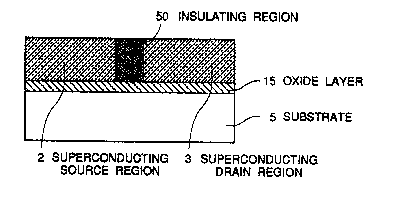
Upper surfaces of ~e insulating region 50, the super~onducting
source region 2 and the supercondwcting drain region 3 are made at the
25 same level. By this, the extremely thin oxide superconductor thin film 1
which constitutes ~he sl~perconducting chamlel lO can be ~onned flatwise.
This improves ~esolwtk~n of photolithography so that ahe gale insulating
i
16
2~3~
layer 7, ~he gate electrode 4, the source electrode 12 and the drain
electr~de 13 can be accurately formed using photolithography. ~n
particular, the gate insula~ing layer 7 and the gate electrode 4 should bc
accurately formed in size and position to obtain the excellent
S perfonnance. The above structures of the insulating region 50, the
superconducting source region ~ and the superconducting drain region 3
malce the fine processing possible which is needed to accurately folm the
gate insulating layer 7 and the gate electrode 4.
Figllre 2 shows a sectional view of a variation of the above
10 mentioned super-FET. The super-FET shown in Figure 2 has an
insulating region SO of which the width of the top portion is narrower
than that of the boteon~ portion and of which the tilt angles a of ~he sides
are 30. Th~ inclined si~es of the insulating region 50 impro~e the
conductanee of superconducting current flowing from the
15 superconducting source region 2 into the extremely thin superconducting
channel 10 and flowing from the extren ely thin superconducting channel
10 to the superconducting drain region 3. For this purpose, ~e tilt angle~
a of the sides of ~he insulating region 50 are pre~era~ly smaller ~an 40C.
If the tilt angles or~ are lar~er than 45~, the superconducting current does
2 0 not flow so efficiently. It is not necess~ry that the tilt angles ot are thesame. Each of the tilt angles a preferably has a different value which is
required by the characteristics of the superconducting current flow, or
the superconducting source region and the superconducting drain ~gion.
In order to ~orm the insulating region 50 having sides ~f which the
2 5 tilt angles a are smaller than 40D, the ion beam is implanted with smaller
incident angle or the subs~rate is tilted in an angle range larger than 4S so
~at the largest angle of incidence of the ion ~eam to the normal 1ine o~
17
2B~9f,~
~e Y1Ba2Cu307 x superconductor ~hin ~llm 11 is no~ smaller ~an 45~ ~d
the smallest angle of incidence is more less than -45 in the process shown
in Figure lC.
The other points of the super-FET are the same as those of the
5 super-FET shown in Figure IH.
Embodiment ~
Re~erring to Figures 3A to 3H, a second embodiment of the process
for manu~acturing the super~onducting device will be described.
In this second embodiment, ~he same processings as ~hQse shown in
Figures lA is per~ormed. After the PrlBa2Cu307.y oxide layer lS is
formed on the substrate 5, a c-axis oriented Y~Ba2Cu30~ ,~ oxide
superconductor thin Fllm 21 is deposited on the Pr]Ba2Cu307 y oxide layer
1~ by an MBE, as shown in Pi~ure 3A. The YIBa2Cu3(:)7.x oxide
superconductor thin film 21 is fon~ed successively to the Pr1Ba2Cu30
oxide layer 15 by switching the Pr molecular beam source to a Y
molecular beam source under a substrate temperature of 700 qC so as to
have a thickness of 50 nanome~ers. A condition of forrning ~he
YIBa2Cu307 x oxide superconduc~or ~hin film 21 by an MBE is as ~ollows
2 0 Molecular beam source Y: 12$0C
and its crucib~etemperature Ba: 600C
C~l: 1040q~ ~.
Pressure I x 10-5 Torr
Thereaf~er, as shown in Fi~gure 3B, a Ga ion beam is imp3~1~ted to a
2 5 ccnter portion of the Yl33a2(: U307.X oxide superconductor thin ~ilm 21 bya ~cused ion beam ~pparatus with an ener~y of 50 keV so as to fonn an
insulating region 51 haYing a width of 0.75 ~lm. The insula$ing region Sl
18
~2 ~
is ~ormed by scanning the ion beam relative to the substrate 5 on which
the Y1B~2Cu3o7 x oxide superconductor thin film 21 is formed so as to
completely divide the YlBa2Cu307~x oxide superconductor thin ~llm 21
into two psrts. In this connection, it is preferable that the ion beam
implantation is successively carried out aîter the deposition of the
YlBa2Cu3O7 x oxide su~erconductor thin film 21 by using an MBE
apparatus whicb posses3es a focused tOII beam gun. The insulating region
51 preferably has a width of from 0.6 to 1.0 llm. If the insulating region
51 is narrower than ~0 nanometers, tunnel current may flow ~tween ~e
10 two parts beyond the insulating regioll 51. As explained hereinafter, dle
insulating region is formed so as t~ have a narrow spacing at the top.
Therefo}~, in order to insure a sufficient spacing at the top, the insulating
r~gion 51 preferably has a width at lea~t 0.6 ~m. If the insulating r~gion
is wider than 1.0 ~n, the size of the device becomes so large that it is not
1~ favorable ~or high density integration. The energy of the ion beam is
preferably 30 to lO0 keV. If the energy of the ion beam is lower th~n 30
keV, the insulating re~ion does not ~ompletely divide the YlBa2Cu3O7.,~
oxide superconductor thin film 21. If the energy of the ion ~am is
higher than 100 keY, the sur~ace of the YlBa2Cu3O7.x ~xide
2 0 superconductor thin film 21 is destroyed and e~hed away.
Then, another c-axis oriented YIBa2Cu307 x oxide supercotad~ctor
thin f11m 22 is deposited on the YlB~2Cu3O7.x oxide superconductor ~in
lm 21, as ~.hown in Figure 3C. The YIBa2Cu307 x oxide superconduetor
thin ~llm 22 is ~ormed by a MBE under the same condition as that of dle
2 5 YlBa2Cu307.x oxide superconductor thin ~llm 21 so as to have the same
thickness as that of the Yl~a2Cu3C)7.x oxide superconductor thin film 21.
19 i.
2C199~
Thereafter, a Ga ion beam Is implanted to a center portion oî the
Y~Ba2Cu3O~ x oxide superconductor ~hin film 22 by a foeused ion beam
apparatus with an energy of 50 keV so as to form an insulating r~gion 52
having a width of 0.50 ,um, as shown in Figure 3D. The insulating region
5 52 is formed ~o be little narrower ~an the insulating region 51.
Repeating the above process, an oxide superconductor layer which
is divided into a superconducting s~urce region 2 and a supereonducting
drain region 3 by an insulating region 50 having a narrow spacing at the
top, as shown in Figure 3E. In this embodiment, the abo-~e process is
l 0 repeated four ti~es. Namely, the YlBa2Cu3O7 x oxide superconductor
thin film having a thickness of 50 nanometers is deposited ~nd the
insulating region is forrned at the center portion of the YlBa2Cu3O7.x
oxide superconductor thin film by an ion beam implantation four times,
so that a superconducting source region 2 and a superconducting drain
1 S region 3 having a thickness of 200 nanometers are formed.
~ n the aboYe mentioned process, each of the c-axis ori~nt~d
YIBa2Cu307 x oxide superconductor thin films pre~erably has a ~ickness
of 30 to 70 nanometers. If ~he oxide superconductor thin films are
thinner than 30 nanome~ers, many repetition of the p~ocess is nece3~ary
20 for ~orming the superconducting sour~e region 2 and the superconducting
drain region 3 having an enough thickness. This results low productivity.
If the oxide superconductor thin films are thicker than 70 nanometers, the
sides of the insuiating region does not have smooth interfaces. In
addition, the required ener~y of ion beam for forming the insulatirlg
25 region becomes larger so that each of the surfaces of the oxide
superconductor thin ~llms may have a danger to be destroyed.
2~ :
2~9~
Thereafter, as shown in Figure 3F, an extremely thin c-axis
oriented YIBa2Cu307.x superconductor thin ~llm I having a thickness of 5
nanometers is fonned on the insulating region SO, the superconducting
source region 2 and the superconducting drain region 3. The
S YlBa2Cu30~ x superconductor thin ~llm 1 is deposited by an MBE under
the same condition as that of the YIB~2Cu30~ superconduc~or thin film
21. A portion of the YIBa2Cu307.x superconductor thin film 1 on the
insulating region SO becomes a superconductin~ channel 10.
Then, as shown in Figure 3a, a gate electrode 4 of Au and a ga~
10 insulating layer 7 of SrTiO3 are formed by the same process ~s
Embodiment 1. The width of the gate electrode 4 and the gate insulating
layer 7 are preferably longer than that of the insulating region SO at the
top to obtain good proper~ies~
Finally, as shown in :Figure 3H, metal source and drain electrodes
15 l2 and 13 of Au are formed on the superconducting source region 2 and
the superconducting drain region 3~ With this, the super-FET m
accordance with the present invention is completed.
In the aboYe menlioned method in accordance wi~h the pre~ent
invention, no etching process is necessary to define the channel a~a from
2 0 an oxide superconductor ~hin film. TherefoFe, oxide superconductsr tbin
lms of the super-FET manufactured by the above method are not
degraded, so that the oxide superconductor thin films have good
superconducting charac~ristics.
In particular, in the above process, the insu]ating region which
25 divides the oxide superconductor thin film into the superconducting
sour~e region and the superconducting drain region is formed by
repeating processes of fo~ning a thin oxide superconductor thin ~llm and
21 `.
2a~f3~la
of implanting an ion beam to its center portion so as tO fonn an insul~ting
region. Since the oxide superconductor thin films are thinner, ~e energy
of the ion beam can be lowered so that the surfaces ~f the oxid~
superconductor thin films are free from degradation. The repeating
S processes can be carned out in one chamber so th,at the interfaces between
the oxide superconductor thin films substantially disappear and th,e oxide
superconductor thin fill~lS are substantially continuous.
In addi~ion, the insulating region ~0 has a narrow spacing at the top.
The inclined sides of the insu]ating region 50 improve the conductarlce of
I û the superconducting current flowing from the superconducting source
region 2 into the extremely thin superconducting channel 10 and flowing
from the extremely ~hin superconducting channel lû to the
sup~rconducting drain region 3.
Since the superconducting channel 10, the part of the
1~ superconducting source region 2 and the part of the superconducting
drain region 3 are formed of c-axis oriented o~ide superconductor thin
fillms, the above mentioned super-PET manu~actured in accordance with
the embodimen~ of the method of the present invelltion has no undesi~ble
resistance nor undesirable Josephson junction between the
superconducting chamlel 1~ and the superconducting source region 2 and
between the superconduct;ng channel 10 and the superconduc~;ng drain
~egion 3.
Embodiment 3
2 5 One variation of the above super~FET will be exp~ained hereinafter.
This variation has tbe s~me shape shown in Pigure 2. The fea~ure of this
variation is that the substrate 5 is formed of a conduetive materials. ln
22 !`;
2a~4a
this embodiment, ~he suhstrate S is fo2~ned of ~b 0.05 wt% doped SrTiO3
having a resistivity of S x 10-2 Qcm. The PrlBa2Cu307.y oxide lay~r lS
not only compensates the lattice mismatch between the substrate and d~e
oxide superconductor, but ~Iso func~ions as an insullating layer. Since ~e
S other structure is the same as the super-FFT shown in Figure 2,
explanations are omitted.
Since the su~strate is forrned of a conductive ma~erial, a subs~rat~
potenti~l can be applied to the super-FET of this structure. 3~y this, the
substrate applied a po~ential can ~hield the super-F~T from the
10 electro-magnetjc field around it, so that the superconducting
characteristics of the super-FET is not affected by devices located near the
super-FET. Therefore, the electric lines of force generated by the
applied gate volt~ge is ~errninated at ~e substrate, so that the super-FET is
hardly affected by a back gate effect caused by the electric field around
l S the super-FET. In this connection, the operation of the super-PET is
stabilized and reliable.
Additionally, since ~e substrate potential has a fixed value, leakal3e
current is preven~ed when a voltage is applied to the gate electrode so as
to isolate the gate completely. The substrate also functions as a magnetic
20 shield of a back plane so that the superconducting portions of the
super-F~T is not affected by magne~ic ~leld ~round the super-FE~T.
By applying a voltage sign~l to the substrate corresponding to ~e
vol~age signal applied to the gate elec~rode, it is also possible to ~m a
double sided and/or dual gate structure. By this, modulation of
25 superconducting current flowing through the superconducting channel
becomes easier.
,.
1,
23
2 ~
In the above sllper-FET, the conductive substrate has a resistivity of
10-3 to 106 Qcm. If the resis~ivity of the substrate is made smaller ~an
10-3 Qcm, the substrat~ loses its clystallinity because of excessive dopants.
On the other hand, if resistivity is larger than 106 Qcm, the substra~e
S itself constitutes a capacitance which causes the additional parasitic effec~.The conductive substrate is preferably ~onned of 0.01 to 0.5 wt%
Nb doped SrTiO3 or Fe doped SrTiO3, etc. Tbese materials have similar
lattice parameters to those ~f oxide superconductors. So these substrates
are suitable to grow epitax~al oxide superconductor thin films. In
10 addition, there is no problem of mutual di~fusion between the oxide
superconductor thin films and the substrates.
Figure 4 shows a sectional ~iew of one variation of the super-PET
having a conductive subs~rate. The super~FET shown in Figure 4 includes
a substrate S folmed of 0.~5 wt% Nb doped Srl'iO3 having a re~istivity of
1~ 5 x 10⁻² ncmJ and an oxide layer 15 ~o~ed of PrlBa2cu3o7~y h~vin~8 a
thickness of on the order of 20 nanometers on the substrate 5. The
super-FE'r further includes a swperconducting channel l0 on a center
portion of the oxide layer 15, a superconducting source region 2 fonned
of Y1Ba2(:~u3O7.% superconductor h~ving a thicl~ess of 200 nanome~s
2 0 a left portion of the oxide layer 15, and a superconductlng drain region 3
formed of YlBa~cu3o7-x superconduct~r having a thickne~s of 200
n~nome~ers on a right portion of the oxide layer 15. The supercondllctilag
c~annel 10 is formed of a YlBa~Cu3O7 x superconductor thin film 1
having a thickness of 5 nanometers prolonged on the supercondu~ting
2 5 sour~e r~gion 2 and the supercondu~tin~g drain region 3 A gate insulating
layer 7 of SrTiO3 is formed on the superconducting channel 1~, and a
gate e1ectrode 4 of P~ is disposed on the gate in~ulating layer 7. A sollrce
24
.
2 ~
electrode 12 and a drain electrode of Au are respecti~ely arranged ~n the
superconducting source region 2 and the superconducting drain regi~n 3.
The side surfaces of superconducting source region 2 and the
superconducting drain region 3 are inclined so that superconducting
S current efficiently flows ~rom the superconducting source region 2 into
the extremely thin superconducting channel 10 and efficiently flows from
the extremely thin superconducting channel 10 to the supercondllcting
drain region 3.
Effects of electric fields on the superconducting channels w~re
10 evaluated for the super-FETs having structures shown in Figures 2 and 4.
Two super-FETs one of which had a SrTiO3 substra~e and the other had a
Nb doped SrTiO3 substrate were prepared for each structure. A metal
pad 4~ was fonned on the oxide layer 15 besides the superconductitlg
channel 10 of each of the four super FETs, as shown in Figure 5.
1 S When a voltage was applie~ ~o the metal pad 40, superconduc~ing
current ~lowing through ~he superconducting channel 10 of each of
super-FETs having SrTiO3 substrates widely fluctuated, so ~hat the back
gate ef~ect was ascertained. On ~he contrary, superconducting current
flowing through the supercollducting ehannel 10 of each of super-FE~Ts
2 0 having Nb doped SrTiO3 substrates varied within 1 %, even if a voltage
of i4~ Y was applied to the metal pad 40. By this, it could be ascertained
that the super^FET having a conductive substrate in accordance with the
present invention had sta~le charac~eristics.
In dle aboYe mentioned embod;ment, the oxide superconduct~r thin
25 film can be formed of no~ only the Y-Ba-Cu-O compound oxide
superconductor material, but also a high-TC ~high critical tempera~re)
oxide super~onductor material, particularly a high-Tc copper-oxide type
2~
~09~6~
compound oxide superconduc~or material, for example a Bi-Sr-Ca-~u-(~
compound oxide superconductor material, and a Tl-Ba-Ca-Cu-O
compound oxide superconductor material.
The invention has thus been shown and described with reference to
S the specific embodiments, However, it should be noted that the pr,esent
invention is in no way limited to the details of the illustrated structures
but converts and modifications may be made within the scope of the
appended claims.
~6