Note: Descriptions are shown in the official language in which they were submitted.
2~97~8
2309-33-00
ULTRA PURE SIL~CON CARBIDE AND HIGH TEMPERATURE
SEMICONDUCTOR PROCESSING EQUIPMENT MADE THEREFROM
CROSS REFERENCE TO RELATED COPENDING APPLICATIONS
This application is a continuation-in-part of 07/979,965
filed November 23, 1992; and Serial No. 07/959,880 filed October
13, 1992, which in turn is a continuation-in-part of Serial
No. 07/923,077 filed July 31, 1992, now abandoned.
BACKGROUND OF THE INYENTION
1. Field of the Invention
The present invention is directed to ultra or very high
purity, monolithic, free-standing silicon carbide which is
produced by chemical vapor deposition under very carefully
controlled conditions, and applications of such CVD-SiC for
various high temperature semiconductor processing equipment,
particularly furnace furniture (e.g. wafer boats, process tubes,
cantilever paddles or rods, and dummy wafers) and wafer handling
equipment (e.g. susceptors, vacuum chucks and transport rings).
2. Description of the Prior Art
Various structural supports and equipment for handling
wafers (e.g. silicon) are required during treatment at elevated
temperatures to manufacture such semiconductor devices as diodes,
transistors and integrated circuits. During such operations
as oxidation, diffusion and deposition of various elements (e.g.
metals) on or into the surface of the wafers, the wafers are
typically heated to elevated temperatures up to about 1350c.
The stock material of choice from which to fabricate various
semiconductor processing furnace furniture and wafer handling
.
2~7~ ~
2309-33-00
equipment would possess excellent thermal shock reslstance,
hic~h mechanical strength, the ability to retain its shape through
a ~arge number of heating and cooling cycles (thermal stability)
and the material must not outgas, i.e. release impurities (dust-
like particles) during loading, processing and unloading of
the wafers in the furnace. Finally the material needs to be
impervious to gases and provide a good barrier to contaminants
(outside environment) to prevent diffusion through the furnace
liner and process tube into the furnace interior. Cleanliness
and control of impurities is the single most important parameter
to the achievement of the ultimate desired electrical performance
in semiconductor devices. High temperature semiconductor
diffusion furnaces used in the processing of silicon (Si) wafers
to make semiconductor devices ~see Fig. 5A-SC schematic)
typically have (1) a furnace liner which is made of quartz,
reaction-bonded (RB) or reaction-sintered SiC with a thin CVD-
SiC coating, or graphite coated with CVD-SiC, (2) a process
tube made of quartz or RB-SiC coated with CVD-SiC, (3) wafer
boats made of quartz, RB-SiC coated with CVD-SiC or graphite
coated with CVD-SiC and (4) a cantilever system onto which the
boats are mounted and inserted into the furnace. The cantilever
system uses either a paddle or rods onto which the boats "sit"
during loading, processing and unloading. See, for example,
U.S. Pat. No. 4,516,897. The paddles and rods are typically
made of quartz or RB-SiC coated with CVD-SiC. The wafer boat
may be fully loaded with the Si wafers to be treated. However,
2~7~8
2309-33-00
should any wafer slots in the boats be unfilled or should various
monitoring or test functions be required, then dummy (false
or imitation) wafers may be used as fillers or product wafer
substitutes. Such dummy wafers are usually made of high purity
material, such as quartz or SiC.
Also various high temperature semiconductor wafer handling
equipment, including susceptors, vacuum chucks and transport
rings, are typically used to load, unload and hold wafers in
the diffusion furnace described. Susceptor plates (see Fig.
6A and 6B schematic) are typically made of graphite coated with
CVD-SiC. Vacuum chucks (see Fig. 7 schematic) and, in
particular, the suction heads thereof are usually made of
stainless steel and other metals, as well as such ceramics as
aluminum oxide (Al2O3) and SiC. Such suction heads are usually
perforated to allow a vacuum to be established across their
faces. See, for example, U.S. Pat. No. 4,906,011. Transport
rings (see Fig. 8A and 8B schematic) are currently made of quartz
and such ceramics as Al2O3 and SiC. Such wafer handling
equipment is often made of quartz glass (fused silica) because
of its high purity, relatively low cost and ease of fabrication
into the desired shapes. However, the quartz components lose
their mechanical strength and devitrify with time at the hlgh
processing temperatures involved In addition, the quartz
components are susceptible to extreme distortion (change in
shape or dimensions) from frequent heating and cooling of the
material during the wafer processing involved,
2~97~
2309-33-00
and the quartz also does not stand up well to the frequent
cleaning with such solutions as hydrofluoric/nitric acid required
to maintain the ultra pure furnace environment desired. Because
of these shortcomings, such alternative materials as SiC have
been developed.
SiC has been shown to be an excellent choice, especially
for semiconductor processing furnace furniture. See, for
example, U.S. Pat. Nos. 4,761,134; 4,998,879 and 4,999,228.
Such known composite furniture components consist of RB-SiC
coated with CVD-SiC or graphite coated with CVD-SiC. Both the
RB-SiC and graphite substrates are highly impure, containing
numerous contaminants detrimental to quality semiconductor device
fabrication. To help overcome this problem the substrates are
coated with a thin layer of CVD-SiC which provides a diffusion
barrier to prevent contaminants in the substrate material (RB-SiC
or graphite) from outgassing in the semiconductor processing
furnace. However, coating these substrate materials with CVD-SiC
still produces a composite with impurity levels too high and
substantially higher than quartz. Another problem with these
CVD-SiC coated composites i5 that the substrates can outgas
through cracks and pin-holes in the CVD-SiC coating, as well
as diffuse through areas where the coating may be very thin.
It is also known to produce monolithic, free-standing CVD-
SiC, for example, in bulk and in the shape of rods, tubes, etc.,
which are particularly useful in chemical apparatus, including
semiconductor furniture, having atmospheres where high
2~9978~
2309-33-00
temperature and/or chemical inertness are desirable properties.
See, for example, U.S. Pat. Nos. 3,157,541; 3l350,182; 3,686,378;
3,746,496; 3,853,974; 3,943,218; 3,950,479 and 3,961,003. Also
of interest is U.S. Pat No. 4,488,920 showing the production
of monolithic, free-standing CVD-SiC plate-like structures for
use as heat exchange components, and U.S. Pat. No. 4,861,533
showing a similarly produced tubular CVD-SiC structure for use
in ball bonding tools. None of these patents produces the ultra
high purity CVD-SiC sought by and produced according to the
present invention.
Currently the most pure form of SiC is deposited by CVD
from a gas mixture of methyltrichlosilane (MTS), hydrogen (H2~,
and generally an inert or non-reactive gas, such as argon, helium
or nitrogen, argon being preferred. Monolithic, free-standing
SiC is typically made by providing a furnace having a deposition
chamber and a removable mandrel (e.g. graphite) therein, and
pyrolytically depositing SiC from the gaseous mixture on the
removable mandrel. MTS provides both Si and C in stoichiometric
(1:1) ratios. The H2 scavenges chlorine (Cl), producing HCl.
The inert or non-reactive gas acts as a carrier gas for MTS
(which is liquid at ambient temperatures); can be varied to
adjust the gas flow velocity through the furnace as is necessary
to sweep reaction products, such as HCl, from the SiC being
deposited; and acts as a system diluent, preventing undesirable
gas-phase reactions which might introduce impurities into the
deposited SiC. Illustrative of such a CVD-SiC system
20997~
2309-33-00
is U.S. Pat. Nos. 4,990,374; 4,997,678 and 5,071,596.
SUMMARY OF THE INVENTION
-
In accordance with the invention, ultra high purity,
monolithic (bulk), free-standing SiC is produced by CVD under
very carefully controlled conditions. The CVD-SiC produced
has a total impurity level (i.e. the sum of all the metal,
metalloid and non-metal elements shown in Table 1) of about
5 ppm or less, preferably about 3.5 ppm or less, by weight as
measured by glow discharge mass spectroscopy (GDMS).
The ultra high purity, bulk SiC is preferably produced
utilizing the CVD process system as disclosed in aforementioned
parent applicatlons Serial Nos. Q7/923,077 and 959,880
incorporated herein.
The bulk, high purity SiC produced is particularly suitable
for such high temperature semiconductor processing applications
as furnace furniture and wafer handling equipment. Preferred
furnace furniture items include wafer boats, process tubes,
cantilever paddles or rods and dummy wafers. Preferred wafer
handling equipment includes susceptors, vacuum chucks and
transport rings.
BRIEF DESCRIPTION OF THE DRAWINGS
FIG. 1 is a diagrammatic cross-sectional view of a furnace
used to produce CVD-SiC in accordance with the method of the
present invention.
FIG. 2 is an enlarged diagrammatic cross-sectional view
of an injector nozzle extending to the deposition chamber of
2a~9~8~
2309-33-00
the furnace of FIG. 1.
FIG. 3 is a further enlarged diagrammatic cross-sectional
view of the injector nozzle of FIG. 2.
FIG. 4 is a diagrammatic illustration of apparatus used
in the hydrogen feed line to provide substantially oxygen-free
hydrogen to the furnace of FIG. 1.
FIG. 5A is a schematic illustration of a typical
semiconductor diffusion furnace.
FIG. SB is an enlarged schematic view of the wafer boat
furniture used in the FIG. 5A furnace.
FIG. 5C is an enlarged view of the cantilever paddle or
rod-type furniture used in the FIG. 5A furnace.
FIG. 6A is a top schematic view of a typical pancake
susceptor for handling semiconductor wafers.
FIG. 6B is a cross-sectional view of the susceptor through
plane A-A of FIG. 6A.
FIG. 7 is a schematic illustration of a typical vacuum
chuck for handling semiconductor wafers.
FIG. 8A is a top schematic view of a typical transport
ring for handling semiconductor wafers.
FIG. 8B is a cross-sectional view of the transport ring
through plane B-B of FIG. 8A.
DETAILED DESCRIPTION OF THE INVENTION
The present invention provides ultra pure SiC having a
total impurity level of about 5 ppm or less, preferably less
than about 3.5 ppm, by weight as measured by glow discharge
2~9~7~
2309-33-00
mass spectroscopy (GDMS). The total impurity level constitutes
the sum of all the metal, metalloid and non-metal elements shown
in Table 1 below; namely, aluminum (Al), arsenic (As), boron
(B), calcium (Ca), cadmium (Cd), chromium (Cr), copper (Cu),
iron (Fe), potassium (K), lithium (Li), magnesium (Mg), manganese
(Mn), sodium (Na), nickel (Ni), phosphorus (P), antimony (Sb),
titanium (Ti) and zirconium (Zr). Within the semiconductor
processing community GDMS is widely accepted as the most reliable
technique to measure the impurity content of a stock material.
Besides having significantly improved purity, the SiC
produced according to the invention is stoichiometric
(1:1 Si:C ratio), has a cubic (~) polycrystalline structure,
is 100% theoretically dense, has very high thermal conductivity,
high strength, excellent thermal shock resistance and excellent
thermal stability.
Thermal conductivity is strongly dependent on the grain
size and purity of the SiC, i.e., the thermal conductivity
increases with increasing grain size and low impurity
concentration along the grain boundaries. The grain size and,
therefore, the thermal conductivity, is controlled, for example,
by the deposition temperature, pressure, and gas flow rates.
For example, under conditions of high temperature and low MTS
flow rate (which results in low MTS partial pressure), the grain
size increases. Conversely, as the temperature is lowered and
the MTS flow increases, the grain size decreases. SiC produced
in accordance with the invention has a thermal conductivity
'~ .
2~9~780
2309-33-00
of about 300 W/mK or above.
According to the invention the SiC can be produced in
various free-standing sizes and shapes, having particular
application for high temperature semiconductor processing
equipment, e.g. furnace furniture and semiconductor wafer
handling components, and does not need to be coated, laminated,
etc, with other materials. Herein SiC is pyrolytically produced
by chemical vapor deposition (CVD) in the form of free-standing,
bulk bodies of such a purity not heretofore achievable using
very specific and controlled process conditions. Certain
parameters, such as individual gas flow rates may vary according
to the size and design of the particular CVD furnace. It has
been found, however, that such CVD-SiC structures having the
aforementioned impurity level as well as a thermal conductivity
of at least about 300 W/mk, is preferably pyrolytically deposited
in a CVD furnace having a removable mandrel on which deposition
takes place under very strict reaction conditions using the
gas mixture consisting of at least methyltrichlorosilane (MTS)
and H2; in particular: a furnace pressure of between about 180
and about 220 torr, a deposition temperature of between about
1340 and about 1380C, preferably between about 1340 and about
1370C, and most preferably about 1350C, a deposition rate
of between about 1.0 and about 2.0 Jum/min., and an H2/MTS molar
ratio of between about 4 and 10. Furthermore, H2 supplied as
a part of the gas stream is purified so that it contains less
than about 1 part per million (ppm) 2 gas by weight and various
2~7~
2309-33-00
means and techniques are provided to exclude particulate
contaminant material from the deposition chamber. The gas
mixture almost always includes an inert gas, preferably argon,
as a carrier for MTS and in an amount to adjust aerodynamic
properties of the gas stream. However, it is conceivable that
the process might be run using only MTS carried by H2. Although
these specific deposition parameters may fall within broad ranges
described in aforementioned U.S. patents, it is demonstrated
hereinafter, that the very specific set of deposition parameters
set forth above achieve the combination of ultra high purity
and high thermal conductivity not found in any deposition system
shown in the prior art.
With respect to "deposition chamber temperature," what
is meant herein is the temperature as determined in the
deposition chamber in close proximity to the mandrel on which
the silicon carbide is being deposited, although the actual
mandrel temperature may be slightly different. Experience has
shown that temperatures at different locations relative to,
but each closely adjacent the mandrel seldom vary more than
about 5C, and it is assumed that the actual deposition
temperature at the mandrel is within 10C of the probed
temperature.
Thermal conductivity is believed to be relatively
consistent, regardless of method of measurement. Herein, thermal
conductivity is the thermal conductivity as typically measured
by flash lamp techniques.
-ln-
2~9~78~
2309-33-00
Unless otherwise stated, all properties of SiC are measured
herlein at room temperature, i.e., 2~-28C ~293-301K).
Herein, the monolithic (bulk), free-standing SiC produced
is preferably at least 5/1000 inch thick (0.127mm). For purposes
of making high temperature semiconductor processing equipment,
the SiC is preferably deposited to a thickness of at least about
1-3 mm. The SiC body or structure may be partially configured
according to the particular mandrel on which SiC is deposited,
but is generally further configured andtor finished by machine
tooling following deposition. Free-standing SiC signifies a
body that is capable of standing free or on its own~ and is
to be distinquished from SiC thin film coatings (currently its
most common application) which are required to be supported
by and inseparable from a backing material or layer. Thus
free~standing SiC is capable of being handled or manipulated
without a backing support for such subsequent processing as
machining and polishing, if required, in much the same fashion
as RB or sintered castings of SiC. The SiC body may be polished
on a surface or surfaces according to the requirements of the
particular component part made by such conventional means as
lapping using pitch and progressively finer diamond abrasive.
In accordance with the invention, to achieve the
aforementioned degree of purity and high thermal conductivity,
it has been found necessary to substantially exclude from the
deposition chamber both oxygen, which tends to cause deposition
of carbon inclusions, and particulates, which may become
_ 1 1 _
2a9~7~8
2309-33-00
inc:lusions in the deposited CVD. The main source of oxygen
is generally the hydrogen gas, and means and techniques are
utilized to reduce and maintain the presence of oxygen in the
hyclrogen gas stream to less than about 1 ppm. Likewise, means
and techniques are utilized for maintaining the deposition
chamber substantially free of particulates or other possible
inclusions. An exemplary approach to substantially eliminating
oxygen and particulates is described below with respect to Figs.
1-4. It is to be understood that other techniques and means
may be employed to eliminate oxygen and particulates, depending
upon the system used. These Figures only illustrate those
portions of the system which are modified for reducing
particulates, as general CVD systems for depositing silicon
carbide are well known, (see aforementioned patents).
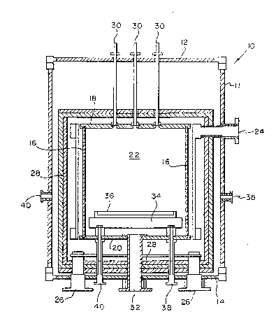
Illustrated in Fig. 1 is a diagrammatic cross-sectional
illustration of a 0.5-m CVD-SiC furnace 10 adapted for depositing
ultra pure, highly thermal conductive SiC according to the
invention. The apparatus includes an outer wall or housing
comprising a cylindrical sidewall 11, a top plate 12 and a bottom
plate 14. An inner wall or housing comprises a cylindrical
sidewall (or isolation tube) 16, a top cover 18 and a bottom
cover 20; the inner wall defines the inner space which is the
deposition chamber 22. Surrounding the isolation tube 16 is
a side heater 24; below the bottom cover 20 is a bottom heater
26. Each of the heaters 24, 26 are of the electrical resistive
type, e.g., being formed of graphite glow bars.
2~97~8
2309-33-00
Interposed between the inner housing and outer housing
ancl surrounding the inner housing and heaters 24, 26 are layers
of lnsulating material 28 which are usually formed of fibrous
material, e.gO, carbon fibers. As will be explained in greater
detail in respect to Fig. 2, these carbon fiber layers 28 are
a source of particulate material, for example, during furnace
assembly; and means are provided for blocking the carbon fibers
as a source of particulate material, for example, during furnace
assembly; and means are provided for blocking the carbon fibers
as a source of particulate material to the deposition chamber.
Injector means 30 provide for entry of gas through the upper
end of the furnace and to the deposition chamber. In the
illustrated furnace 10, three injector tubes 30 are illustrated.
As will be explained in greater detail with respect to Fig.
2, the injectors are a potential source of particulates,
including relatively large particulates, and the injectors 30
in the illustrated furnace have been modified from previous
injector design to eliminate the injectors 30 as a source of
particulate material in the deposition chamber 22. An exhaust
tube 32 communicates with the lower end of the deposition chamber
22.
In the deposition chamber 22 interposed in the flow of
gas, is a baffle plate 34 which is supported just above the
bottom cover 22 in a horizontal orientation. Supported above
the baffle plate 34, also in a horizontal orientation, is the
mandrel 36 on which the bulk CVD SiC is deposited. Deposition
2~997~,3
2309-33-00
charnber 22 temperature is monitored by thermocouples 38 and
optical pyrometers 40.
Although not illustrated in detail herein, the furnace
is assembled through the bottom between each run. During
assembly, there is a tendency for particulates breaking off
from the carbon felt insulation ~8 to contaminate the deposition
chamber 22. To prevent this, protective ceramic blankets or
covers 42 are provided over the carbon felt layers 28. The
cover means 42 illustrated in Fig. 2 comprise cover sheets of
nonporous ceramic gasket material, for example graphite, such
as that sold under the tradename Graffoil, and carbon sleeves
44 capping orifices through the layers 28.
In previous furnace designs, the injectors 30 have been
the source of particulate material which drops onto the mandrel
36 below the SiC being deposited thereon. As diagrammatically
illustrated in Fig. 3, each injector 30 i5 comprised of three
concentric tubes which define annular passageways 56 and 58
and a central passageway 60. The central passageway 60 is the
gas passageway and is open at its lower end to communicate with
the deposition chamber 22. An annular cap 62 extends between
the outer and inner tubes 50,54 sealing the lower end of the
annular passageways 56,58 to each other. The lower end of the
middle tube 52 is spaced above the annular cap 62 to provide
a gap 64 that communicates the annular passageways 56,58. A
coolant, usually water, is pumped downward through the inne_
annular passageway 58 and returns through the outer annular
2 ~
2309-33-00
passageway 56. This coolant prevents deposition from occurring
in the gas flow passageway 60 in the heated region where it
connmunicates with the deposition chamber 22 by keeping the
passageway 60 below the deposition temperature.
It is to be appreciated that each injector tube 30 must
be movable relative to at least the top plate or cover 12 of
the outer housing or the top cover 18 of the inner housing
because of the different temperatures of each of the housings
and the resulting difference in expansion and contraction during
furnace operation. In previous furnace designs (not shown)
the lower end of the injector tubes extended downward below
the top cover 18 of the inner housing and into the deposition
chamber 22 to ensure continual communication between the central
passage of the injector and the deposition chamber. This was
found to be problematic in that the cooler injectors tended
to promote condensation and film build-up thereon, which
deposition might flake off and fall onto the mandrel 36
therebelow and become large particulate inclusions in the SiC
being deposited thereon.
To overcome this problem, the injector tubes 30 have been
positioned or adapted to extend downward to, but not into, the
deposition chamber 22, providing continuous communication with
the deposition chamber, while being relatively slidable relative
to the top plate 12 of the outerhousing. Illustrated in Fig.2
is a preferred design for injector apparatus which provides
for each injector tube 30 extending to, but not into, the
2~7~
2309-33-00
de!position chamber 22. An inlet opening 70 in the top cover
18 of the inner housing is shaped to provide an annular ledge
72. Seated in the opening 70 on the ledge 72 is a carbon washer
74 of appropriate interior diameter that each injection tube
30 seats thereontop. To facilitate seating of each injector
tube 30 on the washer 72 during furnace assembly, a tubular
carbon guide 76 having a tapered upper end 78 also is seated
in the opening 70 on the washer 72. Each injector tube 30
extends upwards through openings 80, 82 in the insulation 28
and top plate 12.
It is important that the openings in the outer housing,
including the opening 82, through which each injector tube 30
extends, be sealed. Accordingly, a flanged sleeve 84 is provided
at the opening 82, fixed to the top plate 12. Each injector
tube 30 is vertically movable through the flanged sleeve 84
to accommodate differential thermal expansion of the inner and
outer housings. A coupling 86 is provided around each injector
tube 30 at a location above the top plate 12. Providing a seal
between the coupling 86 and the flanged sleeve 34 is a bellows
90 that accommodates relative vertical movement between the
top plate 12 and each injector tube 30. To provide for
disassembly and assembly, the illustrated bellows provides for
attachment and separation 88 at two points; 0-rings 88 at these
points provide a gas-tight seal during operation.
As discussed briefly above, another source of inclusions
which detract from uniform deposition of SiC is the presence
2~9~7~
2309-33-00
of oxygen. In examination of previous depositions, small carbon
inclusions could be found. Also, it was noted in SiC depositions
that bands of carbon inclusions tended to form when hydrogen
cylinders were changed, indicating that oxygen might by the
culprit. To avoid changing hydrogen cylinders, sufficiently
large hydrogen cylinders are now being employed to supply an
entire deposition run. Nevertheless, commercially available
hydrogen sources tend to contain amounts of oxygen which, though
very minor, are significant with respect to producing carbon
inclusions in CVD-SiC. Accordingly, to produce the SiC of the
present invention, it was found necessary to purify the hydrogen
gas, particularly to substantially eliminate trace oxygen from
the hydrogen.
Fig. 4 is a schematic of a hydrogen gas line 99 which has
been modified to eliminate oxygen and some other gaseous
impurities continuously from the H2 introduced. The hydrogen
gas line confluences with a flow of argon-carried MTS (not
shown), and the combined flow of argon, hydrogen and MTS is
introduced into the deposition chamber 22 through the injectors
30. The gas line includes the hydrogen source 100. Downstream
from the hydrogen source 100 is a catalytic purifier 102, such
as Resource Systems, Inc., Model RCP-500, which converts oxygen
to water. Dowrstream of the catalytic purifier 102 is a
molecular sieve dryer 104, such as Resource Systems, Inc., Model
MSD-1000, which traps the water This system reduces the oxygen
content of the hydrogen gas stream to below 1 ppm. This system
2~9~
2309-33-00
is also capable of removing carbon dioxide, ammonia and other
undesirable polar molecules. Although this system represents
the preferred method of removing 2 from the H2 gas stream,
other means, such as a gettering system, could be employed for
this purpose.
Fig. SA is a schematic of a well known type high temperature
diffusion furnace 1 used in the processing of wafers 2, e.g.
silicon, to make semiconductor devices. The major components
of this process system are: (1) furnace liner 3, (2) process
tube 4, (3) wafer boats 5 and (4~ cantilever system 8. The
furnace liner 3 is an open ended tube which acts as a barrier
to separate the process tube 4 from the diffusion furnace 1.
The furnace liner 3 is usually about 65 inches long and aids
in preventing diffusion of impurities which, for example, outgas
from the hot furnace walls, heating elements, etc., into the
process tube 4. The process tube 4 is a closed end tube,
typically about 120 inches long, with gas inlet and exhaust
ports at the closed end and an openable flange at the opposite
end. Wafers 2 are loaded into the flanged end of the process
tube, when opened, then sealed in the tube whereupon the tube
is heated and gases are metered into the tube. Certain of the
gaseous elements diffusa into the wafers at high temperatures
to obtain the desired electrical properties, and any by-products
of the process exit through the exhaust port. Wafers 2 are
held inside the process tube 4 in what are known as wafer boats
5. Fig. 5B is an enlarged schematic view of a typical wafer
. .: . . .
.
2~7~8
2309-33-00
boat as depicted in Fig. 5A. There are numerous well known
boat designs, which are usually about 6 inches long; however,
all of the different designs have a common feature of holding
a plurality of wafers in evenly spaced slots 6 machined into
the walls or rails 7 of the boats. The cantilever system 8,
usually about 120 inches long, is used to load and unload the
wafer boats 5 into the process tube 4. The cantilever system
uses either a paddle 9 or parallel rods 13 (two per set) mounted
to an end cover plate (not shown~ onto which the wafer boats
sit during loading, processing and unloading. Fig. 5C
illustrates an enlarged view of the cantilever paddle or rods
schematically depicted in Fig. SA. The wafer boats 5 are placed
on the paddle 9 or rods 13 and then slid into the process tube
4 on a rail system (not shown). The cantilever and cover plate
is then sealed to the process tube flange (open end).
Fig. 6A is a top view of a well known pancake type susceptor
45 having a central opening for handling semiconductor wafers.
Fig. 6B is a cross-sectional view of disc shaped susceptor plate
45 shown in Fig. 6A through plane A-A. Susceptors are typically
used to heat wafers, e.g. silicon, during various processes
known in the art for making semiconductor devices. A plurality
of wafers are typically placed in recessed pockets 46 (seven
are shown) in the susceptor plate, which is then loaded into
a processing chamber (not shown), typically made of quartz.
The wafers are then heated, for example, by coupling
electromagnetic energy (usually RF or infrared energy) into
--1 q--
2~9~7'?~
2309-33-00
the susceptor plate which heats the plate and wafers.
Fig. 7 is a schematic illustration of a vacuum chuck 47
for handling semiconductor wafers 2 which are frequently
transported robotically from one process station to another.
Ideally the vacuum chuck is perforated and made of a lightweight,
stiff, high purity material, as previously indicated, that can
be fabricated with an optically flat surface. Also the material
should maintain its flatness after repeated heating and cooling
cycles during processing.
Fig. 8A is a top schematic view of a typical transport
ring 48 having a central opening for handling semiconductor
wafers. A cross-sectional view through plane B-B of Fig. 8A
is shown of the transport ring 48 in Fig. 8B. The transport
ring is a fixture to support a wafer during processing and
transport from one process station to another. The transport
ring material should be highly pure to prevent contamination
of the wafer during semiconductor processing, exhibit good
thermal stability, be light weight and strong, and machinable
to high tolerances.
As indicated above, the ultra high purity CVD-SiC produced
in bulk according to the invention satisfies the above identified
criteria, and it has been found to be especially applicable
stock material for fabricating the above mentioned furnace
furniture and wafer handling equipment in place of the prior
art materials previously discussed. The benefits of such a
substitution include: (1) reduction of undesirable contaminants
-2n-
2~9~7~
2309-33-00
in semiconductor devices, (2) more reliable semiconductor
devices, (3) lower semiconductor processing costs and (4)
improved semiconductor device performance.
As aforementioned, it has also been found that the CVD-
SiC according to the invention has special application as dummy
wafers in which purity i5 a critical requirement. At the
elevated temperatures involved, various contaminants can diffuse
into or onto the semiconductor product wafers during processing
and adversely change their electrical and optical properties.
For example, during oxide deposition on silicon, any alkali
metal and iron ions would be treated as impurities and should
be avoided. Similarly Group II and IV trace impurities would
be considered detrimental to III-V compound semiconductors.
Dummy wafers are used, for example, as filler wafers and for
monitoring and test purposes~ In the filler application, the
empty spaces in a boat carrying product wafers may be filled
with dummy (false or imitation) wafers. This is standard
technique in semiconductor fabrication and is useful in
maintaining proper flow dynamics inside the reaction/deposition
chamber since gaps and holes in the wafer boat would adversely
change the flow characteristics of the reactive/carrier gas.
In the monitoring and test application, either product wafers
are replaced with or empty boat spaces are filled with dummy
(monitor or test) wafers. It is difficult to run measurements
on product wafers as they, for example, may have multiple
component layers. Whereas a dummy wafer for a particular
2~7~
2309-33-00
component would enable such measurements as growth rate, film
thic]~ness, etc., to be easily read or determined.
ln addition, it has been found that the CVD-SiC according
to the invention has special application as sputtering targets,
evaporation sources and evaporation crucibles or boats which
are used in many physical vapor deposition (PVD) systems for
depositing thin films and coatings.
Comparative impurity measurements performed by GDMS on
CVD-SiC produced according to the invention clearly show that
the overall purity of CVD-SiC is significantly superior to SiC
coated components and quartz as can be seen from the following
table:
:
2~997~
2309-33-00
Table 1
Comparison of trace element impurity levels (ppm by weight) measured inNorton SiC from U.S. Patent 4,998,879; General Electric (GE) Fused
Quartz and the CVD-SiC according to the invention
Impurity ¦ INVENTION ¦ Norton SiC I GE Fused Quartz*
CVD-SiC ! u s Pat. 4,998.879 Type 214 Type 224 LD
AI c0.0091 <10 14 14
As <0.0094 unknown <0.01 <0.01
_
B 0.29 < 10 _ <0.2 <0.2
Ca <0.058 20 0.4 0.4
Cd <0.1~ unknown <0.01 <0.01
Cr <0.1 1 _ 0.05 0.05
Cu <0.016 6 <0 05 <0 01 .
__ . _
Fe c0.04 22 0.2 0.2
K <0.094 unknown __ 0.6 <0.4
Li ~0.003 unknown _ 0.6 <0.001
Mg <0.03 6 0.1 0.1
Mn <0.004 unknown <0.0~ <0.05
Na <0.03 12 _ 0.7 0.1
Ni ~0.013 1 <01 <01
. .
P 0.028 unknown <0.2 <0.2
Sb <0.027 unknown <0.003 <0.003
Ti <0.0042 unknown 1.1 1 .1
Zr <0.0032 unknown 0.8 0.8
Totals <0.90891 <88 1<19.~73 1<17.734
._
* Data obtained from GE Fused Quartz Products brochure, Form 7700,
5/92/5M (GE Quark, Marketing & Sales Headquarters, 21800 Tungsten
Road, Cleveland, OH 44117)
--23--
2~97~
23~9-33-00
Note the CVD-SiC according to the invention has greater
than an order of magnitude (factor of 10) less trace element
impurities than the GE quartz and approximately two orders of
magnitude (factor of 100) less than the Norton SiC.
The CVD-SiC according to the invention has been analyzed
at different testinq laboratories on the same sample, and these
results show that total impurity level is very low, i.e. less
than about 5 ppm, and even less than 3.5 ppm, by weight. Similar
results have been obtained on numerous samples from different
CVD runs and different furnaces, i.e. a small research size
furnace and larger 0.5-m and 1.5-m production furnaces.
The invention will now be described in greater detail by
way of specific examples.
Example 1
Conditions were optimized for a 0.5~m and a 1.5-m production
furnace of Morton Advanced Materials, Woburn MA, which conditions
are given in the table below. It is to be appreciated that
chemical vapor deposition furnaces, as are those used in this
example, are custom manufactured, and that specific conditions
of flow rate may vary from furnace to furnace. To produce CVD-
deposited SiC in accordance to the invention, temperature,
pressure, H2/MTS ratio and deposition rate should be within
the ranges set forth below, regardless of specific furnace
design.
2~ 7~
2309-33-00
Process Parameter 0.5-m Furnace 1.5-m Furnace
Furnace Pressure 200 200
(torr)
DeposiOion Temperature 1350 1350
( C)
Gas Flow Rates: -
(slpm)
H2 28 140
Ar 72 550
MTS 5.6 28
Gas Partial Pressures:
(torr)
H2 53 39
Ar 136 153
MTS 10.6 7.8
Deposition Rate 1.5 1.9
~um/min)
H2/MTS Gas Flow Ratio 5 5
2 ~
2309-33-00
Example 2
Using the O.S-m Furnace of Example 1, CVD-SiC is deposited
in accordance with the conditions described in aforementioned
U.S. Pat. No. 4,990,374, column 1~1ines 30-36, i.e.: deposition
temperature 1300C, furnace pressure 200 torr, gas partial
pressures Ar 68 torr, H2 102 torr and MTS 30 torr. The following
table compares properties of the SiC deposited using the
conditions in Example 1 with the SiC deposited in accordance
with said patent. (Values specified room temperature measurement
values (20-25C).
." , '
': :
..
2~.3~97~
2309-33~00
Property Example 1 Conditions 4,990,374 Cond.
Crystal Structure FCC, polycrystalline FCC, polycryst.
Grain Size (Jlm) 17 8
Density (g/cm ) 3.21 3.21
Hardness (Knoop, 2500 2500
g load)
Chemical impurities <5 Unknown
total ppm (Table 1)
Flexural Strength, 430 490
4-point (MPa)
Elastic Modulus 466 Unknown
Coefficient of 2.2 x 10 6 2.2 x 10 6
Thermal l~xpan-
sion (K
Thermal >300 100-145
Conductivity
(W/mK)
Polish~bility <1 ~10
(~ RMS)
2~ 7.~ ~
2309-33-00
Example 3
In a 70 hr. run, CVD-SiC was deposited in a 0.5mm furnace
under the following conditions:
Furnace Pressure, torr 200
Deposition Temperature, C 1350
Gas Flow Rates:
(slpm)
H2 28
Ar 77
MTS 5.9
Gas Partial Pressures:
(torr)
H2 50
Ar 139
MTS 10.6
Deposition Rate, ~m/min 1.5
H2/MTS Gas Flow Ratio 4.7
The CVD-SiC produced has a total impurity level (see Table
1) of less than about 3.5 ppm by wt. and a thermal conductivity
of 304.9 W/mK at 28 C (301 K) and polishable to <1A RMS.
While the invention has been described in terms of certain
preferred embodiments, modifications obvious to one with ordinary
skill in the art may be made without departing from the scope
of the invention.
Various features of the invention are set forth in the
following claims.
,
. .
!
";