Note: Descriptions are shown in the official language in which they were submitted.
MAT-2403 2fl99~~2
COLOR PICTURE DISPLAY APPARATUS
BACKGROUND OF THE INVENTION
Field of the Invention
This invention relates to a driving circuit for
picture display devices such as Cathode Ray Tubes (CRT)
in color television receivers.
Description of the Prior Art
In the field of television receivers, receivers
have been provided with more~and more functions and
picture quality has been clearer and clearer. As a new
mf-38 ~ mat-2403\canapp0l
,,
i
r
CA 02099832 2002-O1-11
MAT-2403 - 2 -
display device, liquid crystal panels are gradually being
adapted besides CRT's.
A driving circuit in accordance with the prior art,
for use with a picture display device in color television
receivers, is explained below.
FIG. 1 is a circuit diagram of an exemplary CRT
driving circuit. In FIG. 1, guns for red, green and blue in
the CRT are driven by respective driving circuits. As circuit
diagrams for the red and blue guns are the same as that for
the green gun, only a circuit diagram for the green gun is
shown in the drawing.
Transistors Q1 and Q2 are connected in cascade. A
capacitor C1 for frequency characteristic compensation and a
series connction of a resistor R1 and a potentiometer VR2 are
connected between the emitter of the transistor Q1 and the
ground. The emitter of the transistor Q1 is connected to the
potentiometer VR1 for low light white balance adjustment via a
resistor R2. A load resistor R4 is connected between the
collector of the transistor Q2 and a power source BH. A video
signal at the collector of the transistor Q2 is led to the CRT
cathode via a resistor R5.
MAT-2403 - 3 -
2099832
The action of the CRT driving circuit mentioned
above and the white balance adjustment are explained in
the following.
As the transistor Q1 and Q2 are connected in
cascade, when the resistor R2 is large enough, the gain
of the driving circuit is expressed as R4/(R1+VR2), where
R4, R1 and VR2 are the resistance values of the resistors
R4 and R1 and the potentiometer VR2, respectively.
Therefore, the gain is adjustable by the potentiometer
VR2.
This driving circuit can be regarded as a d-c
amplifier and its d-c offset amount can be varied with
the potentiometer VR1. White balance adjustment of this
driving circuit is done so that the specified brightness
ratios of red, green and blue are obtained at the two
brightness levels of low light and high light.
That is, a low light reference signal (flat
signal), which level is adjusted at the input of the
circuit, is applied to the input of the circuit so that a
specified brightness (for example, 5% of the green
maximum brightness) is obtained. Then, each
potentiometer VR1 for low light adjustment in the red and
blue channels is adjusted so that the specified red and
blue low light brightnesses are obtained, respectively.
MAT-2403 - 4 -
2099832
Then, a high light reference signal (flat
signal) is applied to the input of the circuit so that a
specified brightness (for example, 60% of the green
maximum brightness) is obtained by adjusting the
potentiometer VR2 for high light adjustment. Then, each
potentiometer VR2 in the red and blue circuits is
adjusted so that a high light white raster is observed on
the CRT screen.
Although adjustment levels for low light and
high light were explained as 5% and 60% of the maximum
brightness, respectively, in the above example, the
adjustment levels are desirably specified so that a good
tracking characteristic for white balance is obtained,
considering light emitting characteristics of red, green
and blue phosphors of a CRT.
However, in the above mentioned circuit, the
potentiometer VR2 for high light adjustment varies not
only the gain but also the d-c offset amount and the
potentiometer VR1 for low light adjustment varies not
only the offset amount but also the gain. As high light
adjustment and low light adjustment affect each other, a
correct adjustment is not obtained unless these
adjustments are repeated.
CA 02099832 2002-O1-11
MAT-2403 -S-
SUMMARY OF THE INVENTION
The present invention relates to a driving circuit for
a color picture display device which includes (1) a means to add
a clamping potential which is the same level as the low light
signal level for adjusting white balance during a blanking
period of the video signal, (2) a means to control the gain, (3)
a means to clamp at the portion where the clamping potential is
added after the former two means (1) and (2) , (4) a means to
blank the portion where a clamping signal was added, (5) a means
to adjust the clamping potential or the d-c offset amount after
clamping, and (6) a means to drive a display device.
An advantage of this invention is that the low light
level, which was once adjusted by adjusting the clamping
voltage, namely, the d-c offset level, does not vary if the high
light level is adjusted by adjusting the gain.
In accordance with another broad aspect, the invention
provides a color picture display apparatus for providing to
display means an output video signal with adjusted white
balance. The color picture display apparatus includes:
(1) assignment means for assigning a first potential
to an input video signal during a blanking period of the input
signal. The first potential is substantially equal to a first
light level. The first light level is used for adjusting the
white balance and the assignment means generates an assignment
output signal;
(2) gain control means for controlling the amplitude
of the assignment output signal to generate a gain control
output signal;
CA 02099832 2002-O1-11
MAT-2403 -5 (a) -
(3) clamping means for clamping the gain control
output signal at a second potential, to generate a clamping
output signal;
(4) blanking means for blanking the clamping output
signal to generate the output video signal; and
(5) means for providing the output video signal to
the display means.
BRIEF DESCRIPTION OF THE DRAWINGS
FIG. 1 is a circuit diagram of a driving circuit for a
color picture display device in accordance with the prior art.
CA 02099832 2002-O1-11
MAT - 2403 - 6 -
FIG. 2 is a circuit diagram of a driving circuit for a
color picture display device in accordance with an exemplary
embodiment of the present invention.
FIG. 3 (a) - (h) illustrate waveforms to explain the
actions in the two examples shown in FIG. 2 and FIG. 4.
FIG. 4 is a circuit diagram of a driving circuit for a
color picture display device in accordance with a further
exemplary embodiment of the present invention.
DETAILED DESCRIPTION OF THE INVENTION
Referring now to the drawings, an exemplary embodiment
of the present invention is explained in detail.
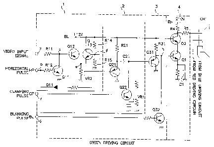
FIG. 2 shows an example of a driving circuit for a
color picture display device (CRT). As the driving circuits for
a red gun and a blue gun are the same as that for a green gun,
only a circuit for the green gun is shown in the drawing.
In FIG. 2, 1 is a low light potential adding circuit,
2 is a clamping circuit, 3 is a blanking circuit, and 4 is an
output circuit to drive a CRT.
CA 02099832 2002-O1-11
MAT-2403 -7-
The actions in each part shown in FIG. 2 are explained
below, referring to FIG. 3 (a). When a video signal like the
waveform a is applied to the video input terminal, the
horizontal blanking period is blanked by the resistor R11 and
the transistor Q11, in which the horizontal pulse HP (waveform
b) for adding the clamping potential is applied. The signal at
the base of the transistor Q12 becomes that as shown by waveform
c. During the horizontal pulse, the diode D11 is off and the
voltage at the base of the transistor Q13 becomes the voltage Ec
defined by the resistors R14 and R15. During the period
excluding the horizontal pulse (scanning period in rough
expression), the diode D11 becomes conductive and the base
potential of the transistor Q13 drops. Thus the waveform at the
base of the transistor Q13 becomes waveform d. The potential Ec
is set to the potential of the low light signal at white balance
adjustment.
As the emitters of the transistors Q12 and Q13 are
connected, the higher voltage between the waveform c and the
waveform d appears at the common emitter of the transistors Q12
and Q13 and the waveform at the emitter of the transistor Q12
becomes the waveform a in FIG. 3 (e). Thus the clamping
potential for low light level adjustment was added to the
blanking period of the input video signal a.
MAT-2403 - 8 -
209832
Then, the signal with the waveform a is divided
by the potentiometer VR2 and is led to the collector of
the transistor Q22 via the emitter follower transistor
Q21 and the capacitor C21.
The transistor Q22 works as a switch by feeding
a clamping pulse (waveform f) to its base, the signal at
the collector of the transistor Q22, which has the same
waveform as e, is clamped at the period (t1-t2) of the
horizontal pulse HP. This clamped level corresponds to
the low light level.
The signal is passed through the emitter
follower transistor Q31 and is blanked at the transistor
Q32, which base the blanking pulse (waveform g) is
applied to. As a result, the signal at the collector of
the transistor Q32 becomes similar to waveform h. The
blanking pulse (waveform g) is added in order to prevent
observing the low light signal on the CRT screen during
the retrace period as result of superimposition during
the trace period.
After that, the signal (shown in waveform h) is
fed to the CRT via the video drive stage, which is a
cascaded connection of the transistors Q2 and Q1, and is
displayed on the CRT screen.
MAT-2403 - 9 -
2oss~3~
A method of white balance adjustment for a
color picture display apparatus (television receivers),
which employ CRT driving circuits mentioned above is
explained.
First, low light adjustment is done as follows.
A low light reference signal (flat signal) is applied to
the television receiver. Observing a waveform at the
emitter of the transistor Q12 in the green channel, the
input signal level is adjusted so that the green input
signal and the added low light level have the same level.
The potentiometer VR1 in the green channel is adjusted so
that the specified low light brightness is obtained on
the CRT screen. Then, each potentiometer VR1 in the red
and blue channels is adjusted so that the specified red
and blue low light brightnesses are obtained,
respectively. Thus, the low light adjustment is.
finished.
Next, the high light adjustment is done as
follows. A high light reference signal (flat signal) is
applied to the television receiver. The potentiometer
VR2 in the green channel is adjusted so that the
specified high light brightness is obtained on the CRT
screen. Then each potentiometer VR2 in the red and blue
channels is adjusted so that the specified red and blue
high light brightnesses are obtained, respectively.
j
MAT-2403 - 10
209~8~2
As the high light adjustment does not affect
the clamping potential of the low light, the low light
adjustment which was finished before does not change.
According to the present invention, because the
following circuits are provided, low light adjustment is
not affected by high light adjustment even if the high
light adjustment is done after the low light adjustment.
(1) a circuit to add the same clamping potential as the
low light white balance adjustment signal during a
horizontal blanking period, (2) a gain control circuit,
(3) a clamping circuit, (4) a circuit to adjust the
clamping level, and (5) a blanking circuit to blank the
previously added clamping signal. Thus, no more
repeating adjustment is needed.
Refering now to FIG. 4, another exemplary
embodiment of the present invention is explained.
The same numbers as that in FIG. 2 are
appointed to the components and circuit blocks which have
the same function as those in FIG. 2. The differences
from FIG. 2 are (1) the clamping potential of the
clamping circuit 2 is fixed and (2) an offset adjusting
circuit comprised of the potentiometer vRi and R14 is
added in the output circuit 2.
MAT-2403 - 11 -
2U998~2
Other than the fact that the low light
adjustment is done by adjusting the d-c offset in the
output circuit instead of adjusting the clamping level in
the first exemplary embodiment, the other functions are
similar to the first exemplary embodiment.
By providing a means to adjust the d-c offset
in the output circuit instead of a means to adjust the
clamping potential in the first exemplary embodiment, an
effect which is similar to that obtained by the first
exemplary embodiment can be obtained.
In the first and second exemplary embodiments,
at the low light white balance adjustment, if the input
terminal of the horizontal pulse is fixed to the d-c
potential for high light adjustment, the whole period of
the video signal is blanked and on the CRT screen the
clamping level itself is displayed. That is, the low
light adjustment can be done with a flat video signal
having a high light clamping potential which is
internally generated instead of a low light reference
signal which is externally applied.
Thus, a low light reference signal becomes
unnecessary, an adjustment between the input signal and
the clamping level becomes unnecessary and the adjustment
procedure is simplified for low light white balance
adjustment.
MAT-2403 - 12 -
209832
In a transparent type display devices such as a
liquid crystal display panel, it may be possible that
high light adjustment is done by d-c level and low light
adjustment is done by gain. The same invention can be
applied if the low light and the high light are
interchanged.
An advantage of this invention is that
repetitive adjustment of low light and high light becomes
unnecessary by providing a means to add a clamping
potential which is the same level as the low light signal
for white balance adjustment during a blanking period, a
means to adjust the gain, a means to clamp at the
clamping potential adding circuit, a means to blank the
added clamping pulse.
The invention may be embodied in other specific
form without department from the spirit or essential
characteristics thereof. The present embodiment is
therefore to be considered in all respects as
illustrative and not restrictive, the scope of the
invention being indicated by the appended claims rather
than by the foregoing description and all changes which
come within the meaning and range of equivalency of the
claims are therefore intended to be embraced therein.