Note: Descriptions are shown in the official language in which they were submitted.
INTEG~ATED MACNETIC READ/WRITE ~ ;
HEAD/FLEXURE/CONVUCl['OR STRIJ(:TIJRE ~:
Background and SummarY of the Invention
This invention relates to an electromagnetic re~d/write structure for the ; ;~
reading and writing of magnetic images on a relatively moving magnetic recording ;~
medium. More specifically~ it relates to a unique, unitary, integrated read/write
head/flexure/conductor structure of extremely small si~-e, and to a method of making the
same. In characterizing the size of the proposed structure, I think of the same as a
micro flexhead.
10While the structure of the invention may be used in a wide variety of
applications, a pre~erred embodiment of the same is described herein in conjunction with
reading and writing images with respect to rigid recording media, such as a disk or drum,
in which application it has been found to have particular utility and to offer special
advantages.
The preferred embodiment of the structure disclosed in the present
specification and claims, and of the formation methodology relating thereto, are
presented herein in the setting of an inductive-type magnetic head (two specific
structural alternatives being shown) havillg construction features that offer what will be
re~erred to herein as common-element reading and writing capab;lity with respect to a
20 magnetic recording meclium. Alternative emb()(liments are ill~lstrated and described
which utilize other types o~ magnetic recording transdLIcer structures, such as magneto~
resistive structures and cross-field structures. In addition, an alternative embodiment
type is described wherein read/wri~te transducer componentry is constructed for divided,
or differentiated, functionality, wherein different specific subcomponentry is employed,
respectively, on one hand for writing information, and on anothel for reading
information relative to a magnetic recording medium.
.. .. , . . . ~ . , . : ............................ - ::
- . . : . .... ~ , . - ,.
Fllrlher, alt~rnative strllctllre is presented and discussed which mixes, ;n the
same overall integratecl constr~lction, m~gnetic read/write trclnsducer componentry which
employs clifferent kinds of magnetically functiollal transdllcer subcomponentry.
The performance of magnetic recor(ling systems improves rapidly as the
separation between the read/write head and the associated recording medium decreases.
In rigid rnedia systems, today, this separation is referred to as "flying height"--a reference
relating to ~he fact that the conven~ional head, often referred to as a slider, is supported
above the rela.tively moving medium surface by an air bear;ng. As the flying height is
reduced, the risk of head wear, and in particular the potential for catastrophic wear or
10 head "crash", increases rapidly. This problem may, of course, be minimized by proper
selection of slider and medium surface materials relating to hardness, coefficient of
friction, thermal conductivity, etc., and also by paying proper attention to the quality of
the head/media interface, lubrication and tile eliminatioll of contaminants which may
appear in that interface.
Nonetheless, in a typical system of this type currently, the head structure
contacts the moving medium in the start and stop process, and occasionally in the
operating mode, resulting, inevitably, in some de8ree of abrasive if not catastrophic wear.
In general, wear rate is dependent wpon surface velocity and appliecl pressure and, for a
given velocity, increases slowly with pressure. However, at some point the wear rate
2~ rises steeply, resulting in some form of catastrophic wear.
One difficulty in understanding the wear process and in limiting wear,
particularly in low flyhlg heads on rigid media, is that the area of contact is frequently
orders of magnitude smaller than that of the "footprint~ of the slider. This is due to one
or more of a variety of factors, such as roll and pitch dynamics, or the presence of a
foreign particle in the head/medium interface. As a conseqllence, the transient local
contact pressure, resulting from applied load plus inertial forces, may become extremely
large. Looking at this situation a bit more closely, a key po;nt is that such microscopic
regions of contact are largely independen~ of the size an~l mass of the sli~ler and, s;nce
reduction of the size and mass of the slicler enables a corresponding reduction in the
applied load and inertial forces, local contact pressure may be reduced accordingly.
Another reason for reducing the footpr;nt of a slider as head/medium
separation is reduced relates to the fact that slider roll or non-~latness of the medium or
slider surface may cause the tip of the read/write pole to be abnormally separated from
the medium.
Reducing the size, mass and applied load of a slider, of course, requires ~;
appropriate attention to the design of the air bearing of the slider, namely, a reduction
lû of the slider's sur~ce corresponding to the reducecl applied load, in order to maintain
the desired flying height. Also to be noted is the fact that the constraint on size and
mass reduction of a slider with conventional designs lies in the practical limitat;ons of
fabricating slider bodies, air bearing rails and gimble-~lexures mechanisms with
appropriately small climensions and tolerances, and mounting the sliders on flexures with
correspondingly tight tolerances. Ultimately, the minimum size and mass ;s determined
by the dimensions of the read/write transducer componentry, electrical conductors and
supporting structure. Present sliders are one to two orders of magnitude larger in size
than the transducer componentry itself, an~l as much as three orders of magnitude larger
in mass. Thus, in principle, the mass, an~ theref()re the local contact pressllre, collld
20 potentially be reduced by abollt three ordels of magllitude, thereby greatly reducing
abrasive wear, and perhaps also eliminating the possibility of a head crash.
In summaly, major advances in the performance of medium magnetic
recording systems may be achieved by furLher reducing head/medium separation--
ultimately to continuous sliding contact. However, reducing hcadlmedium separation,
other things being the same, results in an increasecl abrasive wear, and in a greater risk
of catastrophic wear. Since the area of contact between a slider and a medium is
typically very small and relatively independent of the slider's macrodimensions, it should
be possible to reduce greatly the size and mass of the slider, thus to enable a
corresponding reduction in the applied and inertial forces and the local contact pressure,
all resulting in greatly reduced abrasive wear and lower risk of catastrophic wear.
Reduced footprint dimensions of a slider woulcl also help to maintain small separation
between the head and medium.
A general object of the present invention, therefore, is to provide a unique
read/write structure which deals with each of the issues addressed above in a novel and
extremely effective manner
Specifically, an object of the invention is to provide a unique read/write
10 structure which ;s orders of magnitude smaller in size and mass when compared with
today's counterparts--a structure which is capable of non-catastrophic, continuous sliding
contact interaction with the surface of a relatively moving recording medium.
Yet another ohject of the invention is to provide such a structure which is
characterized by a unitary and totally integrated head/flexure/electrical conductor
combination formed entirely, atom-by-atom, in a deposition process, e.g. by sputtering
and photolithographic patterning of materials.
A relate~ object is to provide a str-lcture of the type generally indicated,
wherein the integrated transducer (head) componelltry can have various specific designs
to suit different specific operational applications. For example, such componentry can
20 include different inductive and/or magneto-lesistive an(l/or cross-field structures, can
include a single- or common-element read/write pole structure with non-differentiated
functionality, and also can include various differentiated-fllnctionality organizations that
feature subcomponentry which is specific for writing and subcomponentry which is
speci~ic for reading, with each such subcomponentry optimized for its specific task, so as
to allow, -for example, highly effective read-after-write type operation, write-wide/read-
narrow type operation~ etc.
2 .L ~
A further object is to provi~e a structure which easily allows for mwltiple-
head arrays. Still an()ther important ol)ject of the invention is to provide a novel method
of manufacturing a read/write structure of the types just generally out}ined.
These and other important objects and advantages which are attained by
the inveneion will become more fully apparent as the description which now follows is
read in conjunction with the accompanying drawings.
Description of the Drawings
Fig. 1 is a working-side perspective (slightly rotated) view of one form of a
read/write structure constructed in accordance with the present invention.
Fig. 2 is an enlarged, longitudinal, lateral cross section of the structure of
Fig. 1 illustrating the integration therein of an inductive probe-type head (transducer
componentry), an electrical coil anci conductive traces connecting therewith, and an
embedding flexure body. The heacl shown here is referred to as a single-element, non-
differentiated f~lnctionality structure designed for common-element reading and writing
of information. ;
Fig. 3 is a plan view taken generally from the bottom side of Fig. 2.
Fig. 4 is a simplified view illustrating the magnetic interaction which oceurs
between the head ;n the struct-lre of Figs. 1, 2 and 3 and magnetic layers of anassociated, relatively moving, rigid recorcling medillm (clisk).
Fig. S is a fragmentary view, somewhat like that of Fig. 2, illustrating an
alternative construction which includes a rnagnetic, common-element, non-differentiated
f.unctionality ring-type read/write heacl (transdllcer componentry).
Figs. 6-13, inclusive, illustrate steps in the manufacture of the structure of
Figs. 1, 2 and 3.
Fig. 14 ~plate 2) is a fragmentary perspective ~non-working side) view of a
multiunit array of structures like the one shown in Fig. 1.
Fig. 15 is a view somewhat like Fig. S illustrating another, alternative,
integrated construction wherein the transducer componentry includes magneto-resistive,
as well as inductive, elements which offer possibilities for divided, or di~ferentiated,
functionality performance.
Fig. 16 is a view also somewhat like Fig. 5 illustrating a further, alternative,
integrated organization wherein the transducer cormpoIlentry includes magnetic cross-
field substructure.
Detai]ed Description of the Invention
Turning now to the drawings, and re~erring first of all to Fig. 1, indicated
10 generally at 20, is a read/write head/flexure/conductor structwre constructed with
transducer componentry prepared in accordance with the present invention. Structure 20
herein has an overall length A of about 0.3-inches, and overall width B of about 0.006-
inches, a thickness C along most of its length of about 0.001-inches, and a somewhat
greater thickness D of about 0.002-inches forming an enlargernent adjacent its left end in
Fig. 1, which end may he thought of as the free read/write working end of the structure.
The opposite, right end of structure 20 in Fig. 1 can be thought of as a mounting end.
The particular dimensions just given have been chosen because they work
part;cularly well. However, I recognize that clifferent specific dirnensions, preferably
generally near the ranges set forth below, can be wsed quite successflllly.
A - 0.2 - 0.5-inches
B - 4 - 20-mils
C- 15 - 60-microns
D - 20 - 65-microns
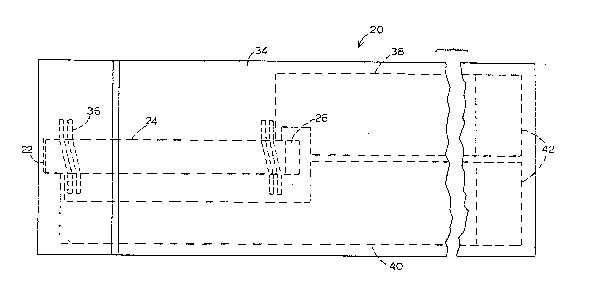
Considering Figs. 2 ancl 3 along with Fig. 1, the magnetic read/write
structure now being describecl is formed with a probe-type head for perpendicular
recording ~both writing and rea(ling utilizing a common element), with this head
including a main pole 22, a yoke 24, a back~gap stud 26~ and a flux-return yoke 28.
6 :
.
t,~ 3'~''
These components are magnetically coupled to form a low-reluctance path, terminating
in a high-reluctance gap 30 between mah1 pole 22 and the end of return yoke 28. This
return yoke may be made preferably somewhat wider than yoke 24 to prov;de a very
large area of flux-coupling and a low-reluctance path to the soft magnetic underlayer of
the record;ng medium With reference for a moment to Fig. 4, such a medium is shown
generally at 32 includillg the just-referred-to soft magnetic underlayer 32a covered with a
high-coercivity, perpendicularly oriented recording layer 32k. ~he direction of motion o
rnedium 32 relative to the head is indicated by arrow 31
The magnetic pole str-lcture (transdLIcer componentry) just generally
10 described is formed in a manner which will be outlined later as a structure embedded
within an elongate, dielectric flexure body 34 which is ma~le herein, for example, of
aluminum oxide. Other flexure-body materials, such as silicon dioxide, may also be used.
Inductively coupled to yoke 24 in structure 20 is a helix coil 36, also
formed in a manner which will be described shortly, with the ends of this coil connecting
~hrough lead conductors 38, 40 to bonding pads 42.
Shifting attention for a moment to Fig. 5, here there is shown an
alternative embodiment of the invention, wherein magnetic structure 20 includes a forrn
of thin film, ring-type head for recorcling (both writing an(l reading utilizing a common
element) on longitudinally oriented medkl, i.e., with an easy axis of magnetization in the
2() plane of ~he media. In this structure there ~re include(l poles 44, 46 which are relatively
thick (in order to avoid pole tip saturation) with their lower extremities substantially
coplanar so as to be in close proximity to the surface of an underlying recording medium.
Gap 48 which exists between these poles is made very small in order to ~ ;
afford good linear bit resolution in signal reproduction. lt is this dimension which
determines ~he linear bit resolution in signal reproduction. Most of the flux, produced
by current flow in the helix coil, bridges directly across gap 48, with only a small part
fringing out to the medium, thus Iimiting the field intensity in the record mode. For this
,, 8
reason, it is necessary to restrict the throat height of gap 4X (the space where poles 44,
46 confron~ and parallel one another) so as to cause more of the flux to encompass the
medium. As a rule of thumb for thin-film, ring-type heads, the ~hroat height is held to
one or two times the gap thickness in order to provi~le sufficiently high field intensity for
recording on high coercivity medîa Thus, in current thin-filrn long;tudinal recording
heads, gap 48 may be about 0.5-micrometers, thereby enabling linear bit resolution of
about 20,000-flux-reversals-per-inch, and restricting throat height to about 1-micrometer.
Higher recording densities necessitate still more precise control of throat height in the
lapping process.
In contrast, gap 30 in the probe type heac3 is made relatively large so that
ve~y little flux in the m~gnetic circuit fringes across this gap. Consequently, virtually all
of the flux from the tip of pole 22 is effective in magnetizing the recording layer ;n the
medium, and there is no similar throat heigllt restriction.
Thus, in practice, the height o~ pole 22 is routinely made about 5- to about
11)-microrneters without deleterious effect on recording and reproducing performance,
though pole tip saturation may become a problem as pole thickness is reduced below
about 0.5- micrometers. From this analys;s, it will be apparent that probe head
recording on two-layer perpendicular media offers great advantage over thin-film ring-
head recording on longitudinal media in regar(l to the ease of hea(l m~anllfactllre and
20 tolerance for head wear as head-media separation is reclllced, ultimately to continuous
sliding contact.
The remainder o~ the magnetic structure shown in Fig. S includes a yoke
50, a back-gap stud 52, and a return yoke 54. Inductively coupled to yoke 50 is a helix
coil 56 which is similar to previously mentioned coil 36. The ends of coil 56 (not shown~
connect to appropriate bonding pads, like pads 42, through connecting conductors, like
previously mentioned conductors 38, 40.
:. :
Those skilled in the art anci familiar with probe-type heads (Fig~ 2) and
ring-type heads (Fi~. S) will understand the magnetic-circuit design constraints which
must be observed in order to have satisfactory head performance. Accordingly, details of
these constraints are not set forth in this description.
The unitary, integrated character of ~he read/write (transducer
componentry) structures illustrated and discussed so far have been achieved in what
might be thought of as an atom-by-atom construction process. One of the most
important constituents of the present invention is that sputtered aluminllm oxide (or
other similar inorganic materials), which is usecl to form the main, elongate embedding
10 flexure body for the entire struct-lre, is characterized by a high degree of elasticity and
structural integrity. This characteristic plays a significan~ role in the ability to offer such
a small-dimension (micro~, low mass (about 100-micrograms) read/write structure. The
structures shown herein are so significantly reclllced in size ancl mass, that experience has ` -
shown that they can be used for direct, continuous, sliding contact operation with a ~ ~ -
recording medium, virtually free from catastrophie wear. ~ ~ -
Considering now the method of manufacture proposed herein for building
structures like those illustratecl, this methocl will be described in conjunction with the ~`
making of the unit shown in Figs. 1-3, inclusive.
As has been mentioned, a key feature of the present invention -- one which
20 marks a fundamental (leparture from conventional practice in the ~abrication and
assembly of heads, flexures and elecLrical connections, lies in the fact that the entire
microhead (transducer)/flexllre/connector complex is fabricated as an integral unit,
utilizing thin-film and photolithographic technology which is widely known by those
skilled in the art. Put another way, the entire structure of the present invention is
~abricated atom-by-atom employing conventional thin--film deposition and etching
processes, e.g., sputtering, vapor deposition, plating, chemical vapor deposition, ion beam
- :
52 ~
deposition and etching, etc., acct)mpanie~l by well known photo-patterning of the
magnetic, electrical and siruct-lral parts.
The magnetic head structure employecl herein, becomes, in a sense~ an
extension of the thin-film reed flexure, and is o~ comparable thickness. Employment of a
helical cnil structure winding around a magnetic yoke enables a very significant reduction
in the physical width of the overall head struct-lre, and more significantly, in the
inductance and resistance of the head and corresponding cross-talk sensitivity. Thin-film
deposition of the electrical leads within the flexllre structure eliminates the need for
bonding twisted-pair conductors as is required in conventional current practice.In Fig. 6., a square waEer 5~, which may be a polished flat wafer of silicon
or ceramic, e.g. barium titanate, serves as a s~lbstrate for the deposition and patterning of
all material which makes up structllre 20 in Figs. 1, 2 an~l 3. Fig. 7 is a fragmentary
section view taken generally along line 7-7 in Fig. 6, illustrating the various layers that
are formed during the construction process to make up read/write structure ~0. With
respect to the way in which structure formation takes place during the manufacturing -
process herein, the upper surface 20a in the struchlre ~see Fig. 2) is what is formed first,
and is the portion of the structure which lies most closely adjacent the upper surface of
wafer 58 in Fig. 6.
Thin films of titanium 60 and copper 62 are sputtered onto the upper
surface of wafer 58, with the former serving as .111 adllesi()n layer, and the latter as an
electrically conducting electro-plating base. A copper layer 64, about 5- to about 25-
micrometers thick, is electroplated over film 62, and polished flat to a smooth, bright
finish. Photoresist is then patterned, forming a rnask through which additional copper is
pla~ed to a thickness of about 6- to abo-ut 10-micrometers to result, after stripping of the
photoresist, in the parallel copper stripes 66.
Photoresist ;s now patterned with reference to edge 58a ~see Fig. 6) of
wafer 58, and about 6- to about 10-micrometers of gold is plated through this pattern to
: :~
,.
J ~
form previously mentioneci bonciing pacls 42 (not shown in Fig. 7). A titanium adhesion
layer 68 is then sputtered over this surface, followed immediately by sputtering of an
aluminum oxide layer 70 to a thickness of ab()ut 6- to about 10-micrometers. The
resulting surface is now lapped and polished to expose stripes 66 and bonding pads 42,
and to form a smooth, plane surface.
Next, a titanium adhesion layer 72 and a plating base 74 are sputtered over
this surface, and photoresist is patterned through which about 2- to about 4-micrometers
of copper are plated, thereby forming the bottom condllctors 76 of previously mentioned -~
helix coil 36. Referrecl to with respect to Fig~ 7 as the bottom conductors of the helix
coil, these appear as the top concluctors in the coil as illustrateci in Fig. 2. This same
layer forms previously mentioned conductors 38, 40, an~l gives ad(led height to stripes 66.
Photoresist is then stripped, ànd again formed and patterne~l to enable subsequent
plating of copper several micrometers thick throuY~h the photoresist mask to form, a~fter
etching exposed parts of plating base 74 and titanium layer 72, electrical via connections
7~, as well as additional copper on top of stripes 66. A titanium aclhesion layer 80 is
then sputtered onto the surface, and subsequently etched through a photoresist mask to
isolate, electrically, conductors 38, 40, all vias 78, and coil condllctors 76. Next, an
aluminum oxide film 82 is sputtered to a thiclcness o~ several micrometers, and lapped
and polished to expose vias 7~3 ancl stripes 6fi, ancl again form a smooth, plane surface.
Following this, another titanillm adllesioll layer X4 and a nickel-iron plating
base 86 are sputtered. Thereafter, a nickel-iron permalloy layer 88 is electroplated
through a photoresist mask, and in the presence of a strong magnetic field, to a thickness
of about 2- to about 3-micrometers thick, to ~orm previously mentioned yoke 24 with a
transverse easy axis of magnetization. This step also extends the heights of vias 78 and
stripes 66.
It should perhaps be noted that the magnetic components in structure 2Q
may be made from various alternative materklls, e.g., cobalt-iron, cobalt-zirconium, iron-
nitride, etc., and by various alternative deposition means, e.g., sputterillg, vapor
deposition, chemical vapor deposition~ etc.
Photoresist is now strippecl and a new photoresist mask is created, through
which nickel-iron layer 90 ;s plated about 4-to about 6-micrometers thick, and again in
an appropriate magnetic field, on top of vias 78 and stripes 66, forming the base of
previously mentioned back-gap stud 26. The exposed areas of layer 84 and base 86 are
etched away, and about 6- to about 8-micrometers of aluminum oxide, layer 92, issputtered over the surface and again lapped and polished to a plane surface, exposing
vias 78, the back-gap stud, and stripes 66. It should be noted that the thickness of
flexure body 34, formed of aluminum oxide, is gradually increasing in this sequence of
depositions, and that the widtll of the flexllre body is limited by the spacing between
stripes 66.
A titanium adhesion layer 94 and a copper plating base layer 96 are
sputtered on the now exposed surface, arld about 2- to about 4-micrometers of copper
are plated through a photoresist mask, thereby to form conductors 98 which interconnect :
vias 78 and cormplete the fabrication of the helix coil, and the connection to the
heretofore isolated conductors 38, 40. After then stripping the photoresist mask just
used, a new thick photoresist mask is prepared, through which about 20- to about 30-
micrometers of nickel-iron, layer 100~ is plated in a magnetic field to ~orm back-gap stud
26, and also to add height to stripes 66. 1'he exposecl areas o~ îilms 94, 96 are etched
away after stripping the photoresist, an(l abo-lt 35- to about 40-micrometers of aluminum
oxide, layer 101, is sputtered over the sur~lce. The sur~ace is again lapped and polished
flat, exposing back gap stud 26 and stripes 66. A titanium adhesion layer 102 and a
nickel-iron plating base lO4 are sputtered to enable a nickel-iron film 106, about 2- to
about 4-micrometers thick, to be plated in an appropriate magnetic field in a photoresist
mask to create previously mentioned return yoke 54. This photoresist mask is then
stripped ancl replaced with a new mask, through which about lS- to about 20-
12
micrometers of nickel-iron, layer IOX, is plateù on top of stripes 66. The exposed areas ~ ~,
of layers 1()2, 104 are etchec~ away, an~l about 15- to about 20-microrneters of aluminum
oxide, layer 110, is sputtered into place, after which it is lapped flat to expose stripes 66.
Finally, the surface of aluminum oxide is etched tlhrough a photoresist mask to a depth - ~
of about 10- to about 15-micrometers, thereby to define the thickness of flexure body 34 ~ ~ -
with the enlargement or step in the surface topography which is present in the region of
gap 30. This etching step also partially exposes the sides of stripes 66. ~:
Scribe cuts 112, about 50- to abowt 100-micrometers deep, and about 100-
to about 150-micrometers wide, are made on the back side of wafer 58 with re-ference to
edge 5~, thereby creating a shallow notch opposite bond;ng pads 42, as is shown in Fig.
11. Saw cuts 114 are now made, clividing wafer 58 into bars 116, exposing the ends of
yoke 24, as shown in Fig. 8, but not exposing bonding pads 42 or conductors 38, 40. Bars
116 are assembled and hekl in a fixture 118 (see Figs. 9 and 10) with epoxy 120, with the
ends of yokes 24 exposed and co-planer with the sur~ace o~ fixture 118. The epoxy fills ~:
previously mentioned notches, or scribe cuts, 112.
The surface of this assembly is then lapped and polished flat. After
cleaning, a soft magnetic film 122 (see Figs. 12 and 13), having a high saturation
magnetization, is sputtered to the desired thickness of previollsly mentioned pole 22 in
the presence of a strong magnetic field so that the easy axis of magnetization is parallel
to the lengths of bars 116, as indicated by arrows 124 in Flg. 12. Filrn 122 is then
patterned, preferably by ion milling through a photoresist mask, to form previously
mentioned poles 22 which join with the exposed ends of yokes 24, as shown in Figs~ 12
and 13~ A passivation layer 126 of aluminum oxide, about 2- to about 4-micrometers
~hick is sputtered over the surface~ Photoresist is patterned and layer 126 is etched,
leaving aluminum oxide covered poles 22 as seen in Figs. 12 and 13. Fixture 118 is then
immersed in a solvent to dissolve the epoxy and to ~ree bars 116. The bars are then
immersed in an etch bath which dissolves the copper and nickel-iron in stripes 66, and
.. , : . ~ ., ::
b~ ~
copper layer 64 underneath the fiex~lre body 34, thereby completing the fabrication of
the structllre of the invention. Finally, run-in lapping serves to expose the tip of pole 22.
Shiftin~, a~tention now frvm the process of man~lfacture proposed herein to
yet another structural implementation of the invention, and directing attention
specifically to Fig. 14, here there is shown, fragmentarily and generally at 128 a
multihead array of individual, independently flexible, head/flexure/conductor structures
arranged as fingers, such as those shown at 12~sl~ 12XI~, 128c~ which extend from anci are
joined through a common support base in~iicated generally at 128d. Each of these
finger-like structures, except where the same joins witl1 base 128d may have the same
10 internal construction as either of the struct~lres shown in Figs. 1 or 5.
Except with respect to the fact that a common support base is included in
such an array, and that photopatterning must take into account the multiplicity of joined
structures, the manufacturing technique employed here is substantially the same as that
just described above.
With respect to the detailed descriptive material presented so far above,
the special utility of the present invention has been describecl particulariy in the setting
of a preferred embodiment wherein, integrclted within the dielectric flexur~ body, there is
a single- or common-element, non-differentiated functionality (for both writing and
reading), readtwrite pole structllre (transducer componentry) which is of the magnetic
20 inductive variety. This preEerred-embodiment setth1g is one wherein the invention has
been found to offer especially widespread utility in today~s most comrnon practices
involving magnetic inforrnation storage. Other practices in other applications, however,
dictate the preferred use of other specific types of transducer componentry in an
integrated structure, and there are several other, well recognized possibilities which are
readily employable.
For example, those skilie~i in the art are aware of the utility, in certain
instances, not only of pole structures which are inductive (magnetic) in nature, but also
14
`y~
of such structures which are flux sensitive, such as those which are magneto-resistive
(magnetic) in nature, and cross-field-operative (magnetic) ;n na~ure. Recognized also by
those skilled in the art is that such pole struct-lres (transducer componen~ries) can be of ~ -
a dual-functionality (or dual-element) type which allows for the respective reading and
writing of information employing different subcomponents that are optimized,
respectively, for these two different functions. Such dual-functionality organizations ~
permit, for example, read-after-write operation and write-wide/read-narrow opera~ion. ~; -
Also, dual-functionality transducer componentries can be ~ormed utilizing different types
(or a mix) of magnetic structures. For example, an integrated, dual-f-lnctionality
10 construction can be made employing both inductive and magneto-resistive
subcompvnentries.
Prior art backgrollnd information regarding certain ones of these other
kinds of integratible transducer componentries is found, for example, in a book by Denis
C. Mee and Eric D. Daniel, entitled "Magnetic Recording", published in 1987 by
McGraw-Hill Inc. (see, as ~m illustration, pages 323-325, inclusive, in that work). U.S.
Patent No. 4,751,598 illustrates and describes an appropriate cross-field structure; U.S.
Patent No. 4,878,140 sets forth magneto-resistive transducer componentry; and U.S.
Patent No. 5,073,836 shows and discusses a divide(l, or differentiated-fullctionality,
sonstruction employing both inductive ~lnd magneto-resistive substructures. The texts of
20 these several materials are hereby incorporated herein by reference.
Figs. 15 and 16 in this document, now to be discussed, illustrate generally
such other kinds of transducer componerltries, and indicate how they may readily be
incorporatecl in the integrated structure o~ the invention. Elements in these drawing
figures are not drawn with elaborate precision, or to scale.
Turning attention to Fig. lS, here there is shown at 130 an integrated
head/flexure/conductor structure constructe(l with dual-functionality transducer
componentry including a ring-type inductive structure 132, which is substantially the same
as that described and illustrate(l with respect to Fig. 5, and a magneto-resistive structure
shown in dashe(l-block outline form at 134. Structures 132, 134 are embodied and
integrated within an elongate dielectric flexure body 136.
The magneto-resistive transducer componentry is located downstream from
ring structure 132 with respect tu the direction of relative media travel, as indicated by
arrow 138. Componentry structure 134 may take the form of any one of a number of
well kns~wn magneto-resistive struct-lres, such as those illustrated and described in the
'140 and '836 patents referred to hereinabove. :
In the embodiment now being described, ring structure 132 is optimized for
10 writing magnetic images, and magneto-resistive structure 134 is optimi~ed for reading
such images. The organization shown thus readily permits not only specifically optimized
dual, or differentiated, functionality performance, but also immediate read-after-write
operation. Further, by proper relative lateral sizing o~ the specific elements which make
up structures 132, 134, the organizat;on illustrated in Fig. 15 can readily be designed for
write-wide/read-narrow operation.
Substantially the same kinds of photo-patterning and photolithographic
techniques described hereinearlier can be used to form the overall integrated structwre
expressed in Fig. 15.
Fig. 15 can also~ and alternatively, operate in this clisclosure to illustrate a
20 dual-functionality transducer componentry construction, in which block 134 represents (in
a very simplified way) an inductive-magnetic type substructure -- thus to emphasize that
dual-functionality performance is readily providable in an integrated structllre wherein
read- and write-optimized elements are generally of the "same" magnetic type. -
Fig. 16 illustrates at 140 another integrated head/flexure/conductor
structure formed in accordance with the present invention -- here employing cross-field
magnetic transdwcer componentry 142 embedded and integrated within an elongate
dielectric flexwre body 144. Cross-field structure 142 may be constructed, as an
16
illustration, in accordance with the teachings of ~he '598 patent cross-referenced herein.
Such cross-~iekl structure has special utility in certain applications vis-a-v;s offering an
enhanced ability to secure magnetic flux extant in a magnetic recording medium.
The statements made above with respect to manufacturing and fabrication
of the integrated structure shown in Fig. lS are applicable also to the fabrication of the
integrated structure illustrated in Fig. 16.
It should thus be apparent that a strikingly unique, integrated, unitary
head/flexure/condLlctor structllre, as well as arrays of such structures, and a unique ~,
method of making the same, are disclosed herein which deals significantly with the size
10 and mass problems that attend use of current read/write structures. The structure of the
present invention can be used in direct, continuous contact with the sur~ace of a
relati~ely moving medium without any appreciable tendency to produce damaging wear.
While a preferred embodiment and method of practicing the invention
have been disclosed, with various alternative pole struct-lres (transducer cornponentries)
illustra$ed, and an array model illustrated, other variations and modifications may
certainly~be made without departing from the spirit of the invention. It will be apparent
also that alternative materials and deposition and patterning processes may likewise be
employed within the scope of the invention.
17