Note: Descriptions are shown in the official language in which they were submitted.
2101328
, ~
GAIN CONTROL CIRCUIT FOR RADIO TRANS~l 1 1 ~;K
Background of the Invention
The present invention relates generally to gain control
~c~h, for radio tran~l,le,s, and, more particularly, to a gain
control circuit for a radio transmitter ope~aLive to transmit modulated
n~1~ in discrete bursts.
A commnnication ~ys~em is operative to transmit
0 inform~t;on (referred to hereinbelow as an "information signal")
between two or more locations, and includes, at a .~ , a
tr~n~mittçr and a receiver interconnecte-l by a cG~ ication rh~nne
A radio comml~nic~tion system is a c~ ~tion system in which
the tr~n~mission rhs~nnel ~. ~;ses a radio-frequency ch~nnel wherein
the radio-frequency ch~nn~1 is ~efine-l by a range of freqllenrie~ of the
com_unication spectrum.
The transmitter, which forms a portion of a radio
co~.. m~ic~t;on system, includes c;~cuit~ for cG.lve~Lil~g the
stion signal into a form suitable for tr~n~mi~sion thereof upon a
20 radio-frequency rh~nnel Suc-h- circuitry includes mod~ t;Qn CilC~Litl~
w_ich ye~rolms a process ~efe~,ed to as modulation. In such a ~oces~,
the inform~tinn signal which is to be transmitted is i ~essed upon a
radio-frequency electromagnetic wave.
The radio-frequency electrom~netic wave upon which the
25 information signal is impressed is of a frequency within a range of
freq -çnries ~lçfining in the radio-frequency ch~nnel upon which the
inform~tion is to be transmitted. The radio-frequency, elecl~o~ gnetic
wave is commnnly referred to as a "carrier ~ign~l," and the radio-
frequency, electromae~letic wave, once modulated by the inform~t;on
30 ~ign~l, is commonly referred to as a modulated siEn~l.
Various modulation srh~mes are known for impressing the
information signal upon the carrier signal to form thereby the
~' 2101328
- 2
mo~ Qte~ sign~ or instance, amplitude modulation, frequency
mo~llll~tion, phase mod~ t;o~, and combinQtiQnc thereof are all
m~ tjQr~ schpmes by whi~h an inform~ion signal may be impressed
upon a carrier wave to form a modulated gi~n~l.
Radio comm~nic~tion systems are advantageous in that no
physical interconnection is required betwee-l the transmitter and the
_iV~:l, once the inform~tiorl signal is mo~ te~l to form a modulated
~iEn~l, the modulated signal may be transmitted over large tli~t~nces.
A two-way, radio communication ~sLem is a radio
cQmmnnication system, ~imil~r to the radio comm~lni~~t;on system
- descnbed above, but which further permits both tr~n~mi~ion of
inform~tion to a location and tr~n~mi~sion of il fo,..~L:Qrl from that
lor~tiQn Each location of such a two-way, radio comm-~nic~tiQn system
c~nt~in~ both a transmitter and a leCeiv~r. The transmitter and
5 lec~;ver positioned ata single location typically co~l;se a unit ~ fel~d
to as a radio transceive., or, more simply, a tra~sceive-.
Conventionally, transceive~ const-. ~,led to be operated in
two-way c~ ;c~tion systems are operative to transmit a mo~-~htecl
signal upon a first radio frequency rh~nnel and to ~eceive a mo~nl~te~
20 signal transmitted upon a second, frequency ~hs-nnel Because ~ien~l~
transmitted to and by such transceive~2 are transmitted upon di~eie..t
radio frequency channels, simultaneous two-way co~ iC~t;on
bet~.ee.- two or more transceive~s is l,e,,nit~ed. ~ien~ls are
~ ously transmitted upon each of the two radio frequency ~h~nr
25 to effect~te the two-way commtmic~tion Such two-way
co~...~ication is oftentimes referred to generally by the term duplex
o~e- ation of the transceiver.
Certain frequency bands of the electroIna~n~tic frequency
spectrum have been allocated for such two-way commllni-c~tinn For
instance, a frequency band e~rten~lin~ between 800 MHz and 900 MHz
has been allocated in the United States for cellular commllnir~tinn
systems. A plurality of radio frequency ch~nnçl~ have been ~lefinetl in
- 2101328
such frequency band permitting operation of numerous cellular
t~1epl on9s (which constitute a type of transceiver construction) thereon.
Convent;~nA11y, transceive.D operative in cellular, co~unication
systems generate modulated sign~1c by a frequency modulation
5 t~chnique. Another frequency band has been ~lloc~te~l for
~ Ati~n by cordless telephones (which constitute another type of
radio transceiver construction).
- Increased popularity of use of such two-way
comm~nic~tion sysl~ms has resulted in increased ~lem~ for access to
0 the finite nt1mber of radio frequency chAnne1~ ~l1oc~ted for such two-
~vay cV~ u~icAt;on .~rhemes have been developed to utilize more
effi~ient1y the frequency bands ~11o~Ate~ for such use.
Several of such srhPmP~s involve the mo~ *ng in en~ od~
form the information sign~l In such a process, the signal becomes
cQmr~cte~l, and the signal may be transmitted more PffiQÇntly (i.e., the
same ~mo~1nt of inform~tion may be transmitted in a lesser a~o~t of
time). Additionally, a modulated signal formed by such a ~rO~8S need
- not be transmitted continuously; rather, the modulated signal may be
transmitted in discrete bursts.
To optimize the use of the available frequency sl,e~ ~l ~, it
i8 often advantageous to modulate both the phase and &,.~ de of a
~ign~1 One guch scheme by which an inform~t;orl signal may be
encoded is a 7c/4 shifted quarternary phase shift keying (1~J4-QPSK)
morl~ ion srhçme. In such a modulation scheme, the information
2s cQntçnt of a modulated signal formed thereby is cont~ine~l in the phase
of the mo~ te~1 si~ns~l Howeve~, rapid phase changes at the data
rates used in these con~mllnications systems results in large frequency
devi~tion~ of the modulated signal which, in turn, results in wide
frequency ch~nne1s. To improve spectrum efflciency, the~b~eb~
modn1~tio~ is frequency limited (filtered). This filtering results in
~ignifi~nt s~mplitude modulation of the modulated sign~l.
210132~
A ~/4-QPSK-modulated signal may be transmitted in
discrete bursts. By transmitting the modulated signal in discrete
bursts, tr~nAmiARiQn of more than one signal at the same frequency is
l,e~ d. Such a terhnique is referred to as time-division multiple
5 access (TDMA).
Howev~r, as the bandwidth i8 controlled by the amplitude of
a ~J4-QPSK-modulated Ai~n~l, care must be e~ercised when ~mplifying
- such a ~ign~ mplifier circuitry forms a portion of radio transmitter
~,c~ts to ~mplify a modulated signal prior to tr~n~miAsior~ thereof.
Gain control circuitry forms a portion of many radio
tr~nQmitt~r circuits. Such circuitry controls the signal level of the
mo~ t~ gignal transmitted by the radio transmitter circuit, and
typically includes ~mE~lifier c;-c.ul, y for ~mplifying a modulated 8igIlal
applied thereto. By controlling the level of ~mplifit~tion of the ~m~lifier
15 C~ (i.e., by controlling the gain of the ~mplifier ~ ), the
signal level of the ~qmplifie~ mo~ te~l signal tr~nQ~nitte~ by the radio
transmitter may be controlled.
Gain control Cl~u,t,l ~ may be constructed to determine the
average power of a 7r/4-QPSK-modulated sign~l, and the amount of
20 ~nplific~tion of such a modulated signal may be col,t,lolled ~~~o~-s;~e to
such meQsl~rement of average power. However, due to the ~mplit~l~e
m~!~nl~t;Qn cQmponent, measurement of the average power requires
mes~6llrement of the signal level of the modulated signal for a period of
time. Such a required time period prior to a dete....i..~tiQn of the
25 ayl,.o~.;ate amount of gain of the modulated signal ~ ,ellts an
accurate determination of desired gain of the modulated signal until the
lequi~ed time period has elapsed and the desired gain has been
determined.
When utili7ing such convention~l gain control Cil~uitl,~ in
30 a radio transmitter operative to transmit an amplitude mo~ te-l
signal in discrete bursts, the a~ol,liate level of ~mplific~ti~ of the
~mrlifier circuitry can not be determined within the time period
2lO1328
",
- 5 -
col.cs~G~ ng to the initial discrete burst in which the modulated signal
i8 tranBmitted.
Alternatively, while the desired level of gain may be initially
eS*m~te~l such es~im~tion may be in~qCc~rate as such an estim~tion of
desired gain is based upon estim~te~3) and not ~ctl~l, parameters.
What is nPe~lerl, thelefole, is a gain control circuit o~ela~ive
to detel~e quickly the desired amount of gain of a modulated ~ign~l.
S-lmm~ry of the Invention
The present inventiQn~ acco,~liugly, advantageously
provides a gain control circuit for controlling the levels of gain of
ifier circuitry of a radio transmitter.
The present invention further advantageously provides a
1 s gain control circuit for a radio trans_itter which generates an
~mplit.l~? modulated signal in discrete bursts.
The present invention still further advantageously provides
a mPtl o-l for controlling the level of gain of ~mrlifier ~l~Uil,~ ~ of a radio
transmitter.
The present invention provides further advantages and
fea~u,es, the ~let~ils of which will becQms more &l,pale.lt by re~ ng the
etPile~l description of the preferred emho~im~pnt~ hereinhelow.
In accordance with the ~,ese"t inventior, the,efole, a gain
control circuit for a radio transmitter is disclosed. The radio
transmitter is operative to generate an information signal in discrete
bursts wherein the information signal generated during at least one of
the discrete bursts includes a pre-deter_ined sequence of data, and the
variable gain amrlifier circuit fol"~i-lg a portion of the transmitter
~,,c~-,t,~ of the radio transmitter is operative to form an ~mplifierl signal
in discrete bursts corresponding to the discrete bursts in which the
inform~tinn signal is generated. The values of the _agnitude of the
amrlifietl signal are measured, and a signal ,~ese.~t~tive of the
measured values is generated. The times when the zqmrlified signal
fo,,l.ed by the variable gain ~mrlifier circuit co ,l"ises the pre-
2101328
- 6 -
detennined ~equence of data are ~lPtecte~l The envelope characteristics
of the ~mplifie~ signal are determined at least during times when the
~mplifie~l gignal formed by the variable gain ~mplifier co~ ;ses the
pre det~l~e sequence of data. The gain charactenstics of the variable
5 gain ~mrlifier are altered Lesl,ollsive to dete,~lle values of the envelope
characteristics of the Amplified ~ignAl
- Bnef Description of the Drawings
0 The present invention will be better understood when read
in light of the accompanying dl~lgs in which;
FIG. 1 is a srhemAtic lel~leEe~ ior illustrating the
tiQn~hip between a mo~ Ated signal generated by a co.lvt:~tional,
co.-t;..~svc-wave modulation technique and a modulated signal
generated by a modlllAtion terhni~-ue ~e.~tlill trAncmi~Rion of the
motl~ l signal in discrete b~ s;
FIG. 2 is a schem~tic ,e~lc~e~.t~t;on of a slot fo,~l~ a
portion of a modulated sign~l;
FIGs. 3A and 3B are sch~m~tic represent~tiQn6~ simil~r to
that of FIG. 2, but illustrating slots formatted accvlv~ g to the formats of
particular communication systems;
FIG. 4 is a graphical le~l~scnt~tion of the envelope of a slot
form~tte-l in a manner, and utili7ing ~/4-QPSK modulation, shown in
the srhem~tic represent~tion of FIG. 3A;
FIG. 5 is a graphical ~eple6cntation, ~imil~r to that of the
gr~phir~l ~ep~escntation of FIG. 4, but illus~l~tillg, in eYr~n~ed form, a
portion of the envelope of FIG. 4;
FIG. 6 is a graphical ~aplesçnt~tion of an envelope
~mplifie~ by ~mplifier circuitry and an envelope of a desiret
amplification level;
FIG. 7 is a simplified, block diagram of the gain control
circuit of a first p~ afeL ~ ed embodiment of the present invention;
- ' 2101328
~_ - 7
FIG. 8 is a block diagram of the gain control circuit of a
second ~lefe.l-~d embo-iimPnt of the present invçntiQn;
FIG. 9 is a block diagram of a radio transceiver of a
~.~fe,~ed ~mho~liment of the present invention which includes the gain
control circuit of FIG. 8; and
FIG. 10 is a logical flow diagram listing the method steps of
a me~l~Qd of a l,lefe~led çmbofliment of the present illve~L on
Description of the Plefe,led F.mho-limPntc
0
In a conventional radio transmitter, a modulated signal is
generated by a cQntinl~ous-wave mod~ tinn technique, and tbe
modulated signal is transmitted contimlously to transmit the mQ~ te~
ignal upon a tr~ncmissio~ ch~nnel. In a cullve~tion~l radio
L~ce;ver~ comp,;sed of both a radio transmitter portion and a radio
;ve~ portion, a modulated signal is ~mil~rly generated by a
cont;nl~ous-wave modulation tec_nique and transmitted continuously.
A mo~ tetl signal transmitted to the radio transceiver, and ,ece;ved by
the radio ,eceivel portion thereof, simil~rly is trangmitted c~ntinlll~llcly
upon a tr~ncmission ch~nnel As both the mo~ te 1 signal
transmitted by, and ~eceived by, a convention~l radio transceivel- are
continllously transmitted, two tr~n~mission ch~nnPls must be ~lloc~te~
to l,el~it two-way commllnir~tion with a conventional radio
tr~n~ceiver.
As mentioned hereinabove, use of radio transc~;vels, such
as cellular telephones, to communication upon a radio commllnic~tion
system has increased dramatically in recent years. Existing frequency
bands allocated for such use have, at times, been utilized at full capacity,
thereby limiting further increases in usage of such radio
cu~u~,ication systems. Accordingly, as also mPntion~ here-in~bove,
schPmes have developed which permit more efficient l-t~ tion of the
eYis*ne frequency bands allocated for such use. In particular,
'' 2~01328
mod~ tion schemPs have been developed to encode and modulate an
i~fo~ t;~n signal thereby to permit the modulated signal to be
tr~n~nitte~ upon a tr~nRmis~ion rh~nnpl in discrete bursts. Two or
more radio transmitters constructed to tr~nRmit modulated ~i~n~ls in
5 such discrete bursts may transmit modulated signsl upon a single
tr~nAmiAsion ch~nn~Al a8 long as the modulated signsl generated by
~ s~.Lv~ ones of of the radio transmitters do not overlap in time. In
such m~nner, the tr~nRmiRsion capacity of e~istin~ loc~tA-l frequency
bands may be increased.
Refemng first now to the st~hAm~tic illustration of FIG. 1,
the r~l~tiQ~Rhip between a modulated signal generated by a
~l~v~ on~l, continuous-wave modulation technique (and, here, in
particular, a frequency modulation technique), and a mo~ tstl signal
formed in a m~nner permitting tr~nRmission thereof in discrete bursts
is shown. The top portion of FIG. 1 shows t~nflemly-positioned blocks
100, 106, and 112. Pictured within bloc~s 100, 106, and 112 is a W~
generated by a conventior ~l, continuous-wave modulation t~chni~lue,
here a frequency-mo~ on technique. A co~vc ~tion~l radio
trans~ll~l constructed to generate and to transmit such a modulated
signal transmits the modulated signal continuously during
tr~nRmiRsinn thereof. As the signal is transmitted continuously, a
single tr~nRmiSsion chs~nnel must be allocated to permit the con~inllo~l6
tr~nRmiR6ion of the modulated si~n~l (A modulated signal generated
by a conventional, continuous-wave, modulation techni~ue to be lece.~,ed
by the l~ceivel portion of a conventional radio transceiver may be
~imils~rly shown.)
FIG. 1 illustrates a three-to-one comp~ction ratio wherein
the information content of the waveforms pictured within blocks 100,
106, and 112 are mapped into block portions 150A, 156A, and 162A,
lesl.e. lively. The waveforrns pictured within block portions 150A, 156A,
and 162A are representative of tnqncmission of a modulated signal in
discrete bursts as the information content of the waveforms pictured
" ~ iO13~8
,
g
within blocks 100, 106, and 112, once encoded, may be transmitted in the
discrete bursts represPnte~ by the waveforms pictured within block
porlions 150A, 156A, and 162A.
While no waveforms are pictured within block portions
150B, 150C, 156B, 156C, 162B, and 162C, suc_ block portions represent
time periods during which other ~ may be transmitted in discrete
bursts.
- When a radio transmitter is operative to transmit a
mo~tll~ted signal in discrete bursts, timing and synchronization
0 conQi~lerations are significant. Modulated sign~l~ transmitted upon a
single tr~n~mi~sion ch~qnn~l cannot be transmitted simultaneously
wit~oul~ inteLre,;~g with one another. Also, a radio lec~;ver operative to
.ece;ve a modulated signal in discrete bursts must be provided
inform~tiQn to permit a determin~tion to be made ag to which si n~l~
~l-ceived by the leceiver in the discrete bursts are to be ~l~motlulated by
the ,ece;vel- and which sign~ ec~;ved by the l~CC;v~:r are to be i~ .lo.ed.
Accordingly, when enco~ing an information signal into
comp~~te~l form, synchroni7~tion information is also i~t.o~ ce~i into the
çnco~e~l si~n~b Such synchronization inform~t;on may, for ~ 9,
con,l,.;se a pre-determined data sequence. A modulated signal
generated and transmitted by a radio transmitter in the discrete bursts
is rec~;ved by a receiver, and the synchronization infor n~tion fc,.~ g a
portion of one or more of the modulated signal portions transmitted in
the discrete bursts is utilized by the radio leceiver for synchror~i7-SIt;on
and t;ming purposes.
Turning now to the sche-m~tic le~lesent~tion of FIG. 2, the
format of a modulated signal transmitted during a time period
corresponding to a single, discrete burst, sometimes ~efe~l~d to as a
"slot", and here referred to generally by reference numeral 200, is
shown. Slot 200 is representative of a modulated signal generated
during a time period represented by block portions 150A, 156A, or 162A
of FIG. 1. As illustrated, slot 200 is comprised of a pre-determined data
21 01328
. ~
- 10-
sequence portion 206 and an information portion 212. Pre-determined
data sequence portion 206 is lel"es~nte~ at a left-h~nd side of slot 200 to
indiC~t~- ~pical positionin~ thereof at a "front end" of the slot. Pre-
de~e,~ed data sequence portion 206 may be c~ ;sed of di~elellt
5 types of data depPn~ing upon system standards of the particular system
in which the signal is trans_itted. For instance, when slot 200
u-~ es the moA~ ted signal portion fol~g the initial signal
~- portion of a transmitted signal (such as the moA~ te~ signal portion
pQRition~ within block portion 150A of FIG. 1), the characteristics and
10 length of data sequence portion 206 may differ with that of a slot fol~g
another signal portion of the transmitted signal (such as the mo~ t
signal portion positioned within block portions 156A or 162A of FIG. 1).
FIG. 3A is a schem~tic represent~t;Qn~ simil~r with that of
FIG. 2, of the format of a slot, here lefell ed to 6_.lelally by lefel e~lce
5 numeral 250, comprising a portion of a moAlll~te~l ~ign~l. Slot 250,
Lo~ el, illustrates the format of a particular cQmm-lnic~tiQn syst m,
here, in particular, a cellular, commnnic~tion system described in
~leater detail in Japan Digital Cellular Standard, RCR STD-27. Slot 250
is ~hown to be cwll~l;sed of an initial block 254, pre-determined data
20 sequence portions 256A, 256B, 256C, and 266D, and inform~tion portions
262A and 262B. Initial period 254 is typically referred to as a "ramp"
period (represented by the letter "R") during which the infol~ t:on
content of the mo~ te-l signal portion 250 is ignored~ Pre-determined
data sequence portion 256A le~re3ents a "preamble" se~nçnt
25 (represçnte~l by the letter "P"); pre-determined data sequence portion
256B represents a "synchroni7~tion word" se~nçnt (lel resented by the
letters "SW"); pre-determined data sequence portion 256C leple~cnts a
"color code" se~nPnt (represented by the letters "CC"); pre-deteImined
data sequence portion 256D represents a "steal flag" se.~ nt
30 (~e~leEe-~te~l by the letters "SF"); and pre-determined data sequence
portion 256E represents a "slow ~Rsoci~ted control rh~nnPl" segrre-lt
(represented by the letters "SAACH"). Information portion segrnPnt~
_ 2101328
- 11 -
262A and 262B cont~in the information cor~terlt of the inform~t;on signal
which is enroA~eA to form a portion of modulated signal portion 250.
I.lfoL~ t;Qn portion se~ments 262A and 262B correspond to inform~t;on
portion 212 of modulated signal portion 200 of FIG. 2.
FIG. 3B is a srhçm~tic represents.tinn~ ~imil~r with that of
FIG. 3A, of the format of a slot, here ~ efe.led to generally by 1efe~,.ce
numeral 300, coml";sing a portion of a mo~ te~ sign~l Slot 300 of
- P'IG. 3B illustrates the format of anot_er particular commllnic~tion
8,~ ~, namely, the format of a slot of a modulated signal generated in a
Aieitpl, cellular, communication system for a Personal Commllnication
Nel-.olL ~iccllcsed in greater detail in Japan Digital Cordless St~n~l~rd,
RCR STD 28.
Modulated signal portion 300 is shown to be com~ sed of an
initial block 304, pre-determined data sequence portion se~n~ntc 306A,
306B, and 306C, and information portion se~ment 312.
Initial period 304, 8imil~r to initial period 254 of mo~nlslt9~l
signal portion 250 of FIG. 3A, is typically lefer.ed to as a "ramp" period
(l~lC~~t9tl by the letter "R") during which the infol..~At;on cort~nt of
the modulated signal portion 300 is ignored.
Pre-determined data sequence portion se~mpnt 306A
1~le~e~ts a "start symbol" se~n-P-nt (l~lere~te~ by the letters "SS");
pre-determined data sequence portion 306B ~el,lesellts a "pre~nnhle"
seEmPnt (represented by letter "P"); and pre-determined data sequence
portion 306C represents a "synchronization word" se~nent (lel.le3e.lted
by the letters "SW"). Information portion segm~P-nt 312 contains the
information content of a portion of the information signal which is
PnroAaA to form a portion of slot 300.
Slots 250 and 300 are two specific e~ Jes of formatv of
which the more generalized slot 200 of FIG. 2 may take. ~f significance
is the prese~ce of pre-determined seqller~ces of data of which portions of
the slots are comprised. As an eY~mple, preamble segments 256A and
2101328
.,._
- 12 -
306B of slots 250 and 300, respectively, may be comprised of a data
8~Q~ -rR of 1001.
The gain control circuit of the ,ulc&lled embo~imPnt of the
~r~DEe.~t invenlion utilizes the çYistçnce of pre-determined data
5 seql~enres, such as the ey~mple of the data sequence 1001 cu~lJ~ising
rre-s-mhl~ sP~Fm~nts 256A and 306B, to determine quickly a desired
Al"~Jl;l;cPt;o~ level of slmplifier cilcuitl~ fol~g a portion of a radio
- tr.s,n~mitt~r. While the specific, pre-dete~ led data sequence portion
may vary depçnding upon the specific fQrmat of a particular
0 c~ ;c~tion system, virtually every commtlnic~tion system having
radio transmitters operative to transmit modulated ~ign~sls in discrete
bursts inrl~ some form of pre-determined data fo~ illg a portion of at
least one of the slots transmitted during one of the discrete bursts.
FIG. 4 is a graphical lel,re~e-~tstion of an envelope of
~verol~ of a slot fOr~llg a portion of a modulated ~ign91~ such as slot
200 of FIG. 2. Ordinate axis 350 is scaled in tenns of a power-related
quanti~y, such as watts or volts, and -s-bscissY axis 356 is scaled in terms
of time, such as, for çy-smrle~ seCon~l~ Envelope 362 lc~rese ~.t~t;ve of a
slot, such as slot 200 of FIG. 2 is, accordingly, a plot of a power-related
qu&lllily plotted as a filnrtion of time.
Envelope 362 is Icl,.csentative of a ~/4 DQPSK-m~ t~
signal fol~.lg a slot having a pre-determined, data sequence portion
and an information portion. The pre-determined data sequence portion,
and here a sequence of 1001 modulated and en~ o~le~ accolLllg to a 7c/4
DQPSK modulation scheme, is formed at a left-hand side portion of the
envelope. Because such portion of the mo~ te~ signal portion, and
hence, the envelope thereof is pre-deterrni~e~, i.e., deterrnin~tive~ a
lcceivt:l operative to receive such a modulated signal is able to detect the
presPn~e of such a data sequence.
The graphical representation of FIG. 5 is similS~r with that
of FIG. 4, but with an abscissa axis çYp~ntle~l in scale. Acco~dingly,
ordinate axis 400 is scaled in terms of a power-related value, and
" 21Q132~
.....
- 13-
~hsrigg~ axis 406 is again scaled in terms of a time value. Envelope 412
is an ~r~ntle~ portion of envelope 362 of FIG. 4. In particular, envelope
412 is ~ ,.~scnt~tive of the data sequence portion of envelope 362 of FIG.
4. Ber~ e the data sequence portion is determin~tive, a leceive
5 operative to lece;ve such a modulated signal is able to detect the
E ~ e of such a predetermined sequence of data.
A modulated signal formed of slots generated in discrete
- bursts is ~mrlified by ~mplifier circuitry of a radio transmitter prior to
tr~nRmis~io~ thereof. The ~mplified~ modulated signal generated by the
0 ~mplifier circuitry of the radio transmitter circuit may also be
ee - .ts~ by the w&vefG~ s plotted in the gr~phic~l .el"escnt~t;on~ of
FIGs. 4 and 5. Measurement of a power-related characteristic of such a
signal is easily made by conventional circuitry, such as a diode power
tectQr. And, the power-related characteristics of the ~ct~
~mplifie-l, modulated signal may be cQmp~red with power-related
characteristics of a desired, ~qmplified~ modulated signal as the power-
related characteristics of the desired, ~mrlifie~l, modulated signal is
determins~*ve.
The power-related characteristic may be any envelope
20 characteristic of the ~mplified~ modulated si~n~l The envelope of the
~mplifie~, modulated signal, over time, is merely the average power of
the ~mplifie~l~ modulated siEn~l. Because the pre-de~...;.~e~, data
sequence portion of a slot is determin~tive~ the envelope of such portion
of a mo~lvl~te-l signal portion is ~imil~rly determin~tive. Accoldi..gly, a
25 peak-to-average power ratio of such an envelope _ay be determin~ 1~ and
such peak-to-average power ratio of an ~ct~ mplifie~l~ mQ~ te~
signal may be comp~red with the peak-to-average power ratio of a
desired, Pmplifie~l modulated si~n~l
Most simply, because the envelope of the portion of a ~lot
30 co ~l,r;sing a pre-deterrnined data sequence portion is determin~tive~ a
correlation may be made between an actual and a desired modulated
signal level merely by detecting the peak power of an ~ctv~ qmplifie~
2101328
.~
- 14 -
mo~nl~te l sien~ql Responsive to such correlation, the gain of the
~mrlifier circuitry may be altered to csuse ~mp1ific~tion of the
m~-ln1~ted signal to form an ~mplified, modulated signal of desired
signal levels.
FIG. 6 is a gr~phictq1 leyl~acnt~tion~ ~imil~r with that of
FIG. 4 wherein a power-related characteristic, here an inst~nt~neous
power level, scaled in terms of milliwatts on ordinate axis 478 is plotted
- - as a f~1nct;~n of time along abscissa axis 456. Envelope 462, p1Otte(l upon
the axis system formed of axes 478 and 456 is representative of a portion
of a slot c~l,l;sing a pre-determined data sequence of a desired signal
level. Envelope 466, shown in hatch, is ~e~les-~tative of the envelope of
a portion of a slot co~ l.sing a pre-determined data sequence of an
actual, ~mr1ifie~l~ modulated sir~l The peak power level of envelope
462 is in~ir~tetl by point 472 on ordinate axis 478; simil~rly~ the peak
power level of envelope 466 is in~ic~te~ by point 450 on ordinate a~cis 478.
The actual and the desired peak power levels of envelopes 462 and 466,
~eL~ec~ ely, may be correl~te~l Responsive to such correlation, the gain
characteristics of amplifier CilC~ forming a portion Of a radio
trans. lit~el may be altered to cause the signal generated by the
~mplifier circuitry to be Of a signal level correspon~ing to a desired
signal level. The graphical l .~ eacntation of FIG. 6 illustrates an
eY~ m ple of which the actual, ~mplified~ modulated signal is of power
levels greater than desired. Accoldillgly, responsive to a correl~t;on of
the actual and desired peak power levels, the gain of ~mp1ifier ~lc lit,
Of the radio transmitter circuit may be loweled.
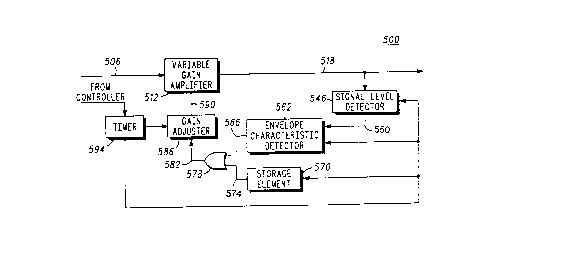
Turning now to the functional block diagram of FIG. 7, the
gain control circuit, referred to generally by ~efel~,-ce numeral 500, of a
first ~ lled embodiment of the present invention is shown in
fi~nc~;on~1 block form. Gain control circuit 500 co~y~es~the signal level
Of a pre-determined data sequence portion of a first slot of a modulated
6ign~1, once amplified by a variable gain ~mplifier~ and co-.-y~- es the
signal level of such pre-determined data sequence portion of a slot
- 15~101328
Pmplifie(l at a desired ~mplification level. Because the pre-determined
data sequence is of a known value -- i.e., signal levels of the w~vefol~ of
the modulated signal portion of the slot cont~ining the pre-determined
data sequence portion ~ct~ y generated can be co...l-A~ ed with signal
5 levels of a correspon~ine portion of a pre-dete.~.ed tata sequence
portion of a slot ~mplifie~ to be of a desired level. As a result of such
co~ ;son, the gain characteristics of the variable gain ~mplifier can
- be altered during tr~ncmi~iQn of the first slot.
Accordingly, a modulated signal (formed of slots generated
in discrete bursts) generated on line 506 is applied to variable gain
amplifier 512. Variable gain amplifier 512 ~mrlifies the mo~ ted
signal applied thereto, and generates an ~mplifie~l modulated signal on
line 518.
Signal level ~l~tector 546 is coupled to lece.ve the ~mplifie~l,
mn-lnl~te-l signal generated on line 518, and is ol,elslive to generate a
signal on line 550 reSp~n~ive to fletecte~l. power-related levels of the
~mplifiP~ modulated signal generated on line 518. The signal
generated on line 550 is applied to envelope characteristic ~ietectQr 562.
Detector 562 is operative to detect a power-related characteristic
responsive to the signal level of the signal applied thereto on line 550. In
a l,.efe,,~d emho~imant~ ~3Ptectclr 562 is ol,elalive to detect the peak
power level of a pre-determined data sequence portion of a first slot of the
modulated si~n~l Envelope characteristic ~letectQr 562 generates a
~ignal on line 566 indicative of such detected value.
Storage element 570 stores a value of a desired power-
related characteristic of a slot amplified at a desired ~mplific~tion level.
The characteristic corresponds with the characteristic detected by
rlPtnctor 562. A signal representative of such value generated on line 574
i8 applied to comp~rator 578. The signal generated by envelope
charactenstic detector 562 on line 566 is also applied to cc.. p~ ator 578.
Comparator 578 compares the values of the siEn~lc applied
thereto on lines 566 and 574 and generates a compQrison signal on line
2101328
- 16 -
582 le~o,lsive to the comparison therebetween. Line 582 is coupled to
gain adjuster 586 which is operative to generate a signal on line 590
which, in turn, is applied to variable gain ~mT)lifier 512. The signal
Arrlie~l to variable gain ~mrlifier 512 on line 590 alters the gain
5 characteristics thereof. The signal generated by gain adjuster 586 on
line 590 is opela~ive to increase or decrease, or to cause to remain
conQtStnt~ the gain characteristics of ~mplifier 512.
Timer element 594 is further illustrated in the functional
block diagram of FIG. 7, and is shown to be coupled to signal level
l o tletect~r 546, envelope characteristic detector 662, storage element 570,and gain adjuster 586. Timer 594 is o~e~ative to generate a signal to
cause o~elalion of detectors 546 and 562, and to cause storage element
570 to generate a signal on line 574, during times in which the pre-
determined data sequence portion of a modulated signal portion is
generated on line 506, and, hence, thereafter on line 518 to cause
o~l~Lon of ~l~tectors 546 and 562, storage element 570, and gain
adjuster 586 during times in which the pre-determined data sequence is
generated on line 506.
Turning now to the block diagram of FIG. 8, the gain
control circuit, referred to generally by reference numeral 600, of a
,lerelled emhoAiment of the present invention is shown. Again, a
mo-lnl~ 3 signal generated by mod~ tiQn circuitry of a radio
transmitter, and formed of slots generated in discrete bursts, is applied
to variable gain amplifier circuitry. Here, the modulated signal is
generated on line 606, and applied to variable gain ~mplifier 612.
Variable gain ~mplifier 612 generates an ~mplifie~l,
modulated signal on line 618 which, here, is applied to mixer circuit 622.
While not shown, an oscillating signal of a desired up-mi~ing~
08~ t;ne frequency is additionally applied to mixer circuit 622. Mixer
circuit 622 generates an up-mixed signal on line 626 which is applied to
power ~mrlifier 630. Power ~mrlifier 630 is operative to amplify further
2101328
,. "~,
- 17-
the signal applied thereto. Power ~mplifier 630 generates a signal on
line 634 which is applied to directional coupler 638.
Line 642 is coupled at a first side thereof to a first line of
dire.~ coupler 638, and, at a secon-l side thereof, to a signal level
~l~tsctor, here diode power (lPte-ct~r 646. Diode 646 is operative to detect
the power levels of the signal generated on line 634 and to generate a
signal in~lir~tive of such ~letected power level on line 650.
- Line 650 is coupled to ~n~log-to-digital conve~ ler 654 which
generates a digitized signal on line 658 which i~ applied to processor 662.
0 Processor 662 contains algorithms operative to ~el~l~u the fil~ct;~ns of
envelope characteristic detector 562, comp~rator 578, and gain adjuster
586 of gain control circuit 500 of FIG. 7.
~çmory element 670 stores values representative of a
desired power-related characteristic, again, ~lefelably, a peak power
level as noted hereinabove, and is coupled to ~loc~ssor 662 by way of line
674. ~ocessor 662 is operative to determine a level of an ~t~
mea~.lred power-related characteristic me~llred by diode 646 with a
value stored by m.omory element 670. Processor 662 further correlates
the two values, and generates a gain adjll.etment signal l~s~o~ ,e to
such correlation on line 690. The gain adjustment signal generated on
line 690 is applied to digital-to-analog collve~ Ler 694, and an ~n~log
signal is generated on line 698. Line 698 is coupled to variable gain
~mrlifier 612 to alter the gain characteristic of the ~mplifier ~s~Gl~i~,e
to the signal level of the signal applied thereto on line 698.
Timer 704 is further illustrated in the block diagra_ of
FIG. 8, and is coupled to processor 662 to cause ~l elc.~ion of the
neceSS~ry algorithms embodied within the processor during times in
which the slots forming the modulated signal generated on line 606
(and, thereafter, the signal generated on line 634) coml,l.ses a pre-
determined data sequence. Because the gain control circuit 600 needs
only to detect a peak power level of a pre-determined data sequence to
determine the desired gain characteristics of variable gain ~mplifier
- 18 - ~ 3 ~ 8 ~s
612, gain control circuit 600 is able to determine quite quickly the desired
gain characteristics of the ~m~lifier 612.
Tu~ing now to the block diagram of FIG. 9, a
radiot~leph-lne, referred to generally by reference nl~meral 780, of a
5 ~lefe~ed embodiment of the present invention is shown.
Radiotelephone 780 is a radio tr~ncceiver having a rece*er portion and a
tr~n~mitter portion wherein the transmitter portion includes the gain
-- control ~c~iL shown in FIGs. 7-8.
The top-half portion of the block diagram of radiotelephone
780 represents the receiver portion of the radiotelerh.~ne, and the bottom-
half portion of the block diagram represents the tra~smitter portion of
the radiotelephone.
The radio receiver portion of radiot~Dlephone 780 is operative
to Lec~ve a modulated signal transmitted thereto. AntDnn~ 784 is
~5 operative to receive the modulated signal trangmitted thereto. ~ntDvnn~
784 c~ve~ ~s the received signal into elechic~l form and generates an
electrical signal indicative of the received signal on line 788. ~ ine 788 is
coupled to filter 790 which generates a filtered signal on line 794. I~ne
794 is coupled to a first input of down-mi2~er 798 to supply an osr~ *n~
signal generated by local oscillator 806 to down-mi~cer 798.
Down-mixer 798 generates a down-milced signal on line 810
which is applied to filter 812. Filter 812 generates a filtered si n~l on
line 814 which is applied to a first input of second down-mi2cer 818 to
supply an oscillating signal generated by local oscillator 826 to down-
mi~er 818.
Down-mixer 818 generates a second down-mixed signal on
line 828 which is applied to filter 830. Filter 830 generates a filtered
sig~al on line 832 which is applied to amplifier 834. ~m~lifier 834
generates an ~rnplified signal on line 836 which is applied to
demodulator 838.
2101328
- 19-
Demodulator 838 generates a demodulated signal on line
840 ~,vhich is applied to ~3ecoAer 842. Decoder 842 generates a tleco~lod
signal on line 846 wbich is applied to a transducer, here spee-ker 848.
The oscillating frequency of the osr~ t;ng signal generated
by os~ t~rs 806 and 826 are m~int~ine~l in a _nown frequency
relot;onchip with reference oscillator 850 by their respective connect
to oSc~ tQr 850 by way of line 852.
The transmitter portion of radioteleF~ n~ 780 is shown at
the bottom-half portion of the figure. An i~fo~ o-1;nr- sign~l~ for
0 in~tonce a voice sign~l, is converted by a tr~nC~llr~r~ here microphone
866, into electrical form, and an electncal signal indicative of such
il~fu~ t;Qn signal is generated on line 860. Line 860 is coupled to
enCo~er 864 which encodes the information signal applied thereto
accoldiL,g to an encoding scheme, such as a 7~/4, QPSK encoding
s~-he-~-e. ~.nco~ler 864 generates an enco~led signal which is applied to
an input of sllmming element 865.
Data sequence generator 866 generates a signal which is
also applied to an input to s~mmer 865. Sllmmer 865 is ~l,e~live to
comhine the .~iEn~ls applied thereto in desired seq~lPnces to form the
fo~nat of a slot, such as those illustrated in FIGs. 2 and 3A-3B.
Sl~.. ;.~E element 865 generates a signal on line 868 which is applied to
filter 872, here a square root raised cosine (SRRC) filter.
Filter 872 generates a filtered signal on line 876 w_ich is
applied to modulator 880. Modulator 880 also ~cceives an os~ g
signal on line 884 generated by oscill~tor 888. Modulator 880 generates a
mo~ tetl signal on line 892 which is applied to filter 896. Filter 896
generates a filtered signal on line 898 which is applied to gain control
circuit 900, represented by the block shown in hatch. Gain control
circuit 900 is simil~r to gain control circuit 600 of FIG. 8.
.C imil~r to gain control circuit 600, gain control circuit 900 is
co~l,L;sed of variable gain amplifier 912, which generates a signal on
line 918 which is coupled to mixer 922. Line 924 is also coupled to _ixer
-20- 2~328 ~
922 to supply an oscil~ n~ signal generated by oscillator 925 to the
miser. Mi~er 922 generates sn up-mi~ed signal on line 926 which is
appIied to power ~mplifier g30. Power ~mplifier 930 generates a signsl
on line 934 which is applied to directional coupler 938.
Line 942 is coupled at a first side thereof to a line of coupler
938, and is coupled at a secon~ side thereof to diode peak ll~tect~r 946.
Diode peak detector 946 generates a signal on line 950 which
- - i8 applied to analog-to-digital converter 954. (~onverter 952 generates a
~igi~e~ signal on line 958 which is applied to processor 962. Memory
elemp~lt 970 is coupled to processor 962 by way of line 974.
Timer 976 further forms a portion of gain control circuit
900, and is coupled to processor 962 and to data sequence generator 866 to
cause operation of the necess~ry algo~ithms e_bodied with~ the
processor during times in which the slots forming the modulated signal
generated on line 898 comprises a pre-determined data sequence.
Processor 962 generates a signal on line 990 which is
applied to digital-to-analog con~/e~ Ler 994. Converter 994 generates an
analog signal orL line 998 which, in turn, is coupled to variable g~un
~mplifier 912 to control the gain characteristics thereof.
Operation of gain control circuit 900 is similp~r with that of
gain control circuit 600 of FIG. 8, and operation thereof will therefore not
be described again in detail.
Radiotelephone 780 of FIG. 9 is further shown to in~ude
line 1002 having a first side thereof coupled to directional coupler 938,
and 8 second side thereof coupled to isolator 1006. Isolator 1006
generates a signal on line 1010 which is applied to filter 1016, and filter
1016 generates a filtered signal on line 1020. Line 1020 is coupled to
antenna 784 permitting tr~nsmission by the antenna of the signsl
applied thereto.
Turning finally now to the logical flow diagram of FIG. 10,
the method steps of a preferred embodiment of the method, referred to
2101328
- 21 -
generally by reference numeral 1100, of a preferred embo~im~nt of the
present invention are listed.
First, and as indicated by block 1106, method 1100 of the
.cd embo~liment of the present invention comprises the steps of
messuring values of the magnitude of the Amrlified signal generated by
a variable gain ~mplifier circuit.
Next, and as indicated by block 1112, a signal l~lescnts~ive
of .... ....r,fi~-~. ed values of the magnitude of the ~mrlifie~ signal measured g the step of measuring is generated.
0 Next, and as indicated by block 1118, times when the
~mplifie~l signal generated by the variable gain ~mplifier circuit
co~yl;ses the predetermined sequence of data are ~letecte~l.
Next, and as indicated by block 1124, envélope
characteristics of the amplified signal are determin~ 3
Finally, and as in~lic~te~ by block 1130, the gain
characteristics of the variable gain ~mplifier are altered le,,~u-~ive to
values of the envelope characteristics of the ~mplified signal determined
during the step of determining.
While the present invention has been de~cribed in
connection with the preferred embo~iments shown in the various
figures, it is to be understood that other Qimil~r emho~ s may be
used and modific~tions and additions may be made to the described
çmhol3imçnts for performing the same function of the present illvellLon
without deviating theleficl.l. Therefore, the yresent ill~,elllion should
not be limited to any single embodiment, but rather construed in breadth
and scope in accordance with the recitation of the sppentle~ cl~imc.