Note: Descriptions are shown in the official language in which they were submitted.
TurrA~z~E op~zcA~ ~zzT~R
Field of the Invention
The invention relates to an optical filter
device, and more particularly to a tunable optical filter
device in which a predetermined wavelength or wavelengths
of an optical signal are selected from wavelength
division multiplexed optical signals.
Baokaround of the Invention
Densely packed incoherent wavelength division
multiplex (WDM) lightwave communication systems are
attractive over coherent (heterodyne) communication
systems because the incoherent system uses the large
wavelength (frequency) domain available in an optical
fiber by assigning different wavelengths to different
channels in the communication system. A key component in
an incoherent WDM lightwave communisation system is the
lightwave receiver which provides filtering,
amplification, and detection of the lightwave signals.
If direct detection is used instead of coherent
detection, tunable optical filters will be needed to
separate the different multiplexed wavelengths (channels)
both for routing and final detection purposes. A WDM
receiver using direct optical detection must optically
filter the multi-frequency WDM signal to pass only the
desired channel or channels to the direct optical
detector. A tunable optical filter therefore has the
function of selecting a predetermined wavelength light
signal from the plurality of multiplexed lightwave
signals. Thus, the goal of a tunable optical filter is
to select one channel (or several channels) in a given
incoming wavelength multiplexed optical signal and block
the other channels from passing through the filter.
2~~.~~.~~.~.
- 2 -
Several different optical filters have been
developed. Fabry-Perot filters with mechanical tuning,
i.e., a piezo-electric element, have been developed.
However, the use of mechanically operated filters has
several disadvantages. First, optical filters with
moving components are typically bulky and are expensive
to produce. In addition, optical filters with moving
components have poor reliability and lower switching
speeds than electronically controlled optical filters.
Optical filters based on acousto-optic TE/TM
mode conversion and waveguides have also been developed.
However, these filters require a relatively complex drive
circuit to generate the required acoustic waves. In
addition, the filters are relatively large with a length
on the order of one to two centimeters. Optical filters
based on semiconductor distributed feedback (DFB) laser
diodes and multi-section Fabry-Perot laser diodes have
also been developed. Such distributed feedback
semiconductor laser structures are operated with a bias
current set below a threshold current for lasing. While
these devices have the advantage of having gain, they
also have several disadvantages. First, the tuning range
of these distributed feedback semiconductor laser devices
is small at less than two nanometers at a wavelength of
1.5 micrometers for a InGaAsP/InP device. Furthermore,
they have a very narraw bandwidth because of the gain and
they are susceptible to saturation effects if the
incoming signal power is too high.
Optical filters based upon a distributed-Bragg
reflection (DBR) laser structure have also been
developed. The distributed-Bragg reflection laser
structure is employed as an integrated receiver within a
lightwave communication system. The DBR laser structure
is biased electrically below the lasing threshold to
operate as a multifunctional element by performing the
integrated operation of resonant amplification and
filtering of the received lightwave signals. By
CA 02101411 2003-03-06
3
electrically biasing the Bragg section of the DBR laser
structure, it is possible to tune the filter so as to
select the desired wavelength. The DBR laser structure has
a larger tuning range, up to 15 manometers, than the DFB
laser diodes, and it can be made insensitive to the power
of the input signal by removing the gain section from the
filter. However, the DBR laser structure operates using
reflection wherein the output signal is reflected back in
the input waveguide, through the input signal, which
l0 results in loss penalties when the signals are separated.
Summary Of The Invention
The present invention discloses a tunable optical
filter for use in a wavelength division multiplexing
system. The optical filter contains a plurality of tunable
reflection gratings which block all of the channels in the
incoming lightwave. The gratings can be tuned so that
their reflection bands do not coincide with a desired
channel or channels thereby allowing the desired channel or
channels to pass through the filter.
In one embodiment of the present invention, the
tunable optical filter has a first semiconductor substrate
which has an electrode on one surface. A waveguide is
formed in and laterally defined within the surface of the
substrate, for carrying lightwaves. A plurality of tunable
reflection gratings are provided on a second surface of the
semiconductor on top of the waveguide. An insulating
substrate is provided on both sides of the waveguide. A
plurality of electrodes control the tunable reflection
gratings so as to vary the effective index of refraction of
a section of the waveguide below each grating.
In another embodiment, the tunable optical filter
comprises: a substrate; a dielectric cladding layer
provided on top of the substrate; a waveguide formed in
CA 02101411 2003-03-06
3a
and laterally defined within the surface of the cladding
layer; and a plurality of tunable reflection gratings
provided on top of the waveguide, each of the tunable
reflection gratings having a heating element for varying an
effective index of refraction of a section of the waveguide
below the grating.
In another embodiment, there is provided a
tunable optical filter for a communication system with a
plurality of channels which comprises: a first
semiconductor substrate having a first electrode provided
on a first surface thereof; a waveguide formed in and
laterally defined within the surface of the substrate, for
carrying light waves; a plurality of tunable reflection
gratings provided on a second surface of the semiconductor
substrate on top of the waveguide, each of the tunable
reflection gratings blocking a particular channel of the
communication system. An insulating substrate is provided
on both sides of the waveguides, and a plurality of
electrodes vary the effective index of refraction of a
section of the waveguide below the grating.
Brief Description Of The Drawings
These and other features and advantages of the
present invention will be readily apparent to one of
ordinary skill in the art from the following written
- 4
description read in conjunction with the drawings, in
which:
Fig. 1 is a cross-sectional view of an optical
filter of one embodiment of the present invention;
Fig. 2 is a transverse cross-sectional view of
the optical filter illustrated in Fig. 1;
Fig. 3 is an explanatory diagram showing the
transmission spectrum of the light that passes through
the filter when no current is applied to the device;
Fig. 4 is an explanatory diagram showing a
wavelength shift to allow a channel through the filter;
Fig. 5 is an explanatory diagram showing a
wavelength shift to allow several channels through the
filter:
Fig. 6 is a cross-sectional view of an optical
filter of another embodiment of the present invention;
and
Fig. 7 is a transverse cross-sectional view of
the optical filter illustrated in Fig. 6.
Detailed Description of the Preferr~d Embodiments
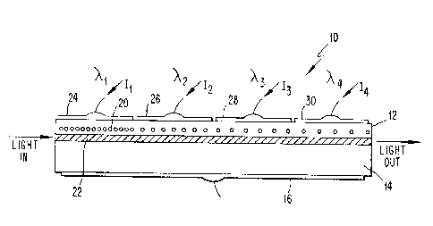
In Fig. 1, there is shown a tunable optical
filter 10 of one embodiment of the present invention.
Fig. 1 illustrates an example of the optical filter for a
four-channel system. The figure is only for illustration
and one of ordinary skill in the art would understand
that the invention is not limited thereto. In this
embodiment, the tunable optical filter is constructed out
of InGaAsP/InP semiconductor material. The layer
structure of the tunable optical filter comprises a
substrate 14 of n-InP material and a layer 12 of p-InP
material. A waveguide 22 is formed between layer 12 and
the substrate 14 and is formed out of an intrinsic
material. A diffraction grating layer 20 is formed in
between the waveguide 22 and the layer 12. In this
embodiment, the waveguide is divided into four sections
since this is a four-channel system. In each section,
the period of the reflection grating is different.
- 5
Electrical insulation, which is not shown in Fig. 1, is
needed in between the different grating sections. The
electrical insulation can be formed by ion implantation
or by replacing the n-InP layer 12 with a semi-insulating
(Fe doped) InP material between the grating sections. In
order to control the refractive index in the four
sections of the waveguide, four electrodes 24, 26, 28 and
30 are formed on top of layer 12. In addition, another
electrode 16 is formed on the bottom of substrate 14.
Finally, as illustrated in Fig. 2, a semi-insulating InP
layer is formed on either side of the waveguide 22 in
order to separate layer 12 from substrate 14. The
optical waveguide 22 is constructed out of a InGaAsP care
which has a bandgap with a shorter wavelength than the
light passing through in order to avoid absorption. The
waveguide 22 is surrounded by InP material so that it
forms a buried hetero structure. The Bragg diffraction
gratings are formed in the layer 20, using InGaAsP and
InP material. This can be done by one of the well-known
methods used in DFB lasers, such as direct electron-beam
writing, etching, and regrowth.
Since the waveguide 22 is constructed out of an
intrinsic core material and the two substrates 12 and 14
are constructed out of p-InP material and n-InP material
respectively, the resulting structure forms a P-I-N diode
structure which allows injection of electrons and holes
into the intrinsic waveguide 22. The semi-insulating InP
layer 18 is used on the sides of the waveguide 20 in
order to confine the current to the intrinsic waveguide.
The injected carriers will change the refractive index of
the waveguide and thereby allow the tuning of the
wavelength of the reflection band of the corresponding
grating. To allow independent tuning of the four grating .
sections, there are four electrical contacts on top of
the p-InP layer.
Typical dimensions for the device described
above would be as follows. The waveguide 22 would have a
thickness between 0.2 and 0.6 micrometers with a width of
approximately 1 micrometer. The layer 12 would have a
thickness between 1 and 3 micrometers with a length for
each grating section between 200 and 500 micrometers.
The electrical insulation between the grating sections
would be between 10 and 50 micrometers. Therefore, the
total length for a four channel example would be between
1 and 2 millimeters.
In accordance with the above-described
l0 structure of the tunable wavelength filter, the principle
in which a transmission wavelength is controlled will be
explained as follows.
In Fig. 3, the transmission of light through
the filter is illustrated as a function of the wavelength
of the light. Bragg diffraction gratings with different
periods block light of different wavelengths from passing
through that portion of the filter. As a result, by
selecting four different periods for the diffraction
gratings, four different wavelength bands of the light
entering into a filter will not be allowed to pass
through the filter as illustrated in Fig. 3. By
selecting the channels of a communication system, i.e.,
~,~, 112, 7~3, J14, to coincide with the wavelengths which are
not allowed to be transmitted through the filter, the
optical filter can control the wavelength signals which
pass through the filter. In the present embodiment, the
gratings are designed so as to block the channels when no
current is applied to electrodes 24, 26, 28 and 30. As
. illustrated in Fig. 4, when a current is supplied, for
example, to electrode 28, the effective index of
refraction of the waveguide section below the section
which had been blocking the third channel is changed so
that the wavelength corresponding to the third channel is
no longer blocked and is allowed to pass through the
filter. As a result, any channel can be selected by
supplying the appropriate voltage to the appropriate
electrode which changes the index of refraction inside
the waveguide.
The grating tuning is based upon a change of
the effective index of refraction. This change can be
achieved in several ways. First, free carrier injection
in the waveguide can be used. The free carrier injection
method uses forward bias in a P-I-N diode structure to
inject carriers into the waveguide. This method is used
in tunable DBR lasers as disclosed in "Semiconductor
Lasers for Coherent Optical Fiber Communications", T.
Koch and U. Koren, Journal of Lightwave Technology, Vol.
8 (3), March 1990, pp. 274-293. Free carrier depletion
in a waveguide can also be used to change the effective
index of refraction. In that case, the InGaAsP material
used for the waveguide 22 should be doped. The free
carrier depletion method uses a reverse bias to sweep the
carriers out of the waveguide thereby changing the
effective index of refraction. The effective index of
refraction can also be changed using electro-optic
tuning. In electro-optic tuning, an electric field
applied through a reverse biased P-I-N structure changes
the refractive index of the waVeguide. This can be done
with bulk material, but quantum wells should probably be
used in order to get a sufficient index change. The
above-listed methods of creating tuning are not meant to
be exclusive since other methods are also possible. For
example, if the filter were made out of dielectric
material, such as Si02 on a Si substrate as described
below, the whole P-I-N diode structure could be replaced
by a simple heating resistance in contact with the
waveguide to change the effective index of refraction by
thermo-optic effect.
In the present embodiment a reflection grating
is provided for each channel in the communication system.
The gratings are designed to block each channel when no
current is applied through electrodes 24, 26, 28 and 30.
Since precise fabricatian of each grating can be
_$_
difficult, i.e., small errors in the wavelength
positioning of the gratings may occur so that a grating
does not block a channel which it is supposed to block,
the filter can be compensated by tuning the grating
through one of the methods disclosed above. Furthermore,
if channel spacing is large enough so that when one
channel is opened the shifted reflection band does not
block a neighboring channel, the filter may allow several
channels to pass through instead of just one. This is
illustrated in Fig. 5, which shows that the gratings
corresponding to channels 2 and 3 have been tuned to let
theses channels through the filter while channels 1 and 4
remain blocked. This can be advantageous when the filter
device is used in a system to perform wavelength
dependent routing.
Another embodiment of the present invention is
illustrated in Figs. 6 and 7. The figures are for
illustration only and illustrate a four-channel filter 60
which is constructed out of dielectric material. In this
embodiment, a silica-based waveguide with a SiOz-Ge02 core
66 is buried in a Si02 cladding 62 on a Si substrate 64.
Tunable reflection gratings 70 are formed on the top
surface of the core 66 by etching the top surface of the
core 66 before regrowing the Si02 cladding 62 on top of
the core 66. In this embodiment, the waveguide is
divided into four sections since this is a four channel
system. In each section, the period of the reflection
grating is different. The reflection gratings 70 are
tuned by thermo-optic effect, wherein the effective index
of refraction of the waveguide section below the gratings
is changed by a temperature change. A heating resistance
is deposited on top of the waveguide section below each
reflection grating so that the effective index of
refraction for each reflection grating can be
independently controlled. It will be understood by one
of ordinary skill in the art that other dielectric
materials, such as Si3N4, can also be used. Due to the
c~ ;1 a
g _
thermal tuning, this embodiment will probably have a
longer switching time and a larger size than the
InGaAsP/InP implementation. However, a dielectric filter
with thermo-optic tuning may still be used in some
applications due to lower fabrication costs.
In another embodiment of the present invention,
a large number of gratings with partially overlapping
reflection bands and a corresponding number of electrodes
are used in the optical filter instead of having one
grating for each channel. The gratings are designed so
as to completely block a wavelength band larger than the
input wavelength band. By designing the gratings to
completely block a wavelength band larger than the band
used, the filter has some tolerance to imperfections in
the fabrication of the filter. The electrodes can then
be used to change the effective refractive index of the
waveguide sections to allow one or several channels to
pass through the filter. This configuration has several
advantages. First, the gratings block the spontaneous
emission noise outside the channels that are caused by
the amplifiers in the system. As a result, a quieter
signal is outputted from the filter. In addition, the
filter can be reconfigured electrically if the channel
configuration of the system changes.
Material and composition of the filter of the
present invention, may be replaced by other semiconductor
materials such as, for instance, AIGaAs/GaAs system
material or dielectric material such as for instance,
TiOz, A120~, etc. Furthermore, the optical waveguide
structure is not limited to planar structure or buried
structure.
It will be appreciated by those of ordinary
skill in the art that the present invention can be
embodied in other specific forms without departing from
the spirit or essential character thereof. The presently
disclosed embodiments are therefore considered in all
respects to be illustrative and not restrictive. The
2~~~~~.~
- to -
scope of the invention is indicated by the appended
claims, rather than the foregoing description and all
changes which come within the meaning and range of
equivalents thereof are intended to be embraced therein.