Note: Descriptions are shown in the official language in which they were submitted.
COMPLEMENTARY LOGIC INPUT PARALLEL (CLIP)
LOGIC CIRCUIT FAMILY
Field of the Invention
This invention relates to integrated circuit
field effect transistor (FET) logic circuits, and more
particularly to high speed, high density complementary
all-parallel FET logic circuits.
Background of the Invention
Complementary Field Effect Transistor (FET)
logic circuits, and in particular Complementary Metal
Oxide Semiconductor (CMOS) logic circuits have become
increasingly popular for integrated circuit logic,
among other reasons because of their high circuit
density and low power dissipation. A typical CMOS
logic gate is illustrated in Figure 1 of U.S. Patent
No. 3,911,29 to Takemoto entitled MOS Type
Semiconductor IC Device. A CMOS logic gate typically
includes a driving stage having a plurality of FETs of
a first conductivity type connected in parallel and a
load stage comprising alike plurality of serially
connected FETs of opposite conductivity type. Each
logic signal input is applied simultaneously to a pair
of transistors, one driver and one load.
Unfortunately, the serial connection of the
load transistors in conventional CMOS logic gates
reduces the toggle rate or switching speed of the gate
CA 02101559 2000-02-16
-2-
and also reduces the number of inputs which may be
applied to the gate (referred to as "fan-in"). To
overcome these problems an "all parallel" CMOS gate
design has heretofore been proposed. One all parallel
CMOS logic gate is described in Figure 3A of the
aforementioned U.S. Patent No. 3,911,289, in which the
serial load transistors are'replaced by a first load
which may be an MOS transistor or a resistor, and a
second load comprising an MOS transistor having
opposite conductivity type from the driver stage
transistors.
A particularly high performance all-parallel
logic family is described in Application Serial No.
07/338,280 filed on April 14, 1989, by the present
inventor, Albert W. Vinal, and entitled High Speed
Complementary Field Effect Transistor Logic Circuits,
now U.S. Patent No. 5,001,367, which is assigned to the
assignee of the present invention.
A
high speed, high density low power dissipation
complementary FET logic circuit is disclosed, in which
the voltage transfer function of the logic gate's
complementary FET inverter output stage is deliberately
skewed to dramatically decrease the lift-off interval
for the logic gate and thereby dramatically increase
the speed of the gate. A switching speed of 500
megahertz or greater may be obtained, which is a factor
of five or more greater than prior art all-parallel
logic designs, for example the design disclosed in the
aforementioned U.S. Patent 3,911,289.
Notwithstanding the above described
improvement, there is a continued need for higher
performance all-parallel logic designs. In particular.,
there is a continued need for a high speed logic
circuit family in which the rise and delay times of the
gate are minimized. In other words, the internal delay
of the date in providing a logic output signal which
CA 02101559 2000-02-16
-3-
accurately reflects the state of the logic input
signals must be minimized.
Another major limitation on the speed of
complementary FET logic inputs is the inherent
difference between the saturation current of P-channel
devices compared to those of N-channel devices. In
particular, silicon P-channel FET devices deliver about
half the saturation current as comparable N-channel FET
devices. The lower saturation current and
corresponding lower carrier mobility of P-channel
device limits the overall speed of the logic gate.
Finally, the internal capacitance of the
logic gate also is a major roadblock in increasing its
speed. The internal capacitance of the gate also
typically limits the number of logic inputs which can
be handled by a single gate (fan-in). Applications
that require large numbers of logical inputs, such as
decoding operations, therefore typically require
"trees" of cascaded logic gates, which dramatically
increase the overall delay time.
Summary of the Invention
It is therefore an object of an aspect of the present invention __
invention to provide a high speed complementary all-
parallel FET logic circuit family.
2 5 It is another object of an aspect of the present invention
to provide a high speed complementary all-parallel FET
logic family which exhibits minimum delay.
It is yet another object of an aspect of the present invention
provide a high speed complementary all-parallel FET
logic family, the performance of which is not limited
by the inherently lower saturation current and carrier
mobility of P-channel FET devices.
It is still another object of an aspect of the present invention
invention to provide a high speed complementary all
parallel FET logic family which exhibits low internal
CA 02101559 2000-02-16
-a-
capacitance so that large numbers of logic inputs may
be handled by a single gate.
These and other objects of aspects are Provided
according to the present invention by a Complementary
Logic Input Parallel ("CLIP") logic circuit family,
which includes a driving stage having at least one FET
of a first conductivity type, with each FET having at
least one control electrode for receiving logical input
signals. The driving stage FETs are connected between
a common output and a first potential level. A
complementary FET inverter, comprising a pair of
complementary FETs, is serially connected between the
first potential level and a second potential level,
with the input of the complementary inverter being
connected to the common output.
According to the invention, at least one
gating FET of second conductivity type is provided,
with the gating FET being connected between the second
potential level and the common input. The control
electrode of the gating FET is connected to the control
electrode of one of the driving stage FETs. The
dimensions of the gating FETs are controlled relative
to the dimensions of the driving stage FETs to provide
a high speed logic circuit. In particular, the ratio
of the channel width of the gating FETs to the channel
width of the driving stage FETs is substantially equal
to the ratio of the square channel saturation current
of the driving stage FETs to the square channel
saturation current of the gating FETs times the ratio
of the channel length of the gating FETs to the channel
length of the driving stage FETs times the number of
gating FETs, divided by 2. Stated mathematically:
Isa td
Zd I' Ld ~ 2
satg
_5_ ~:~~~~'"
where Z' is the channel width of the gating transistors,
Zd is the channel width of the driving stage
transistors, I""~d is the saturation current for a
square channel driving transistor, I'"r~ is the
saturation current for a square channel gating
transistor, Ls is the channel length of the gating
transistors, Ld is the channel length of the driving '
stage transistors, and S' is the number of gating
transistors. It has been found, according to the
invention that when the geometry of the gating FETs are '
arranging as described above, the internal delay time
of the logic gate is dramatically decreased thereby
improving the speed of the gate while still insuring
reliable logic switching.
In a CLIP AND gate, the driving stage
transistors are P-channel FETs and the gating
transistors are N-channel FETs. In a preferred
embodiment of the present invention where the channel
lengths of the driving stage and gating FETs are equal
the above formula reduces to Z" = ZP/2r~ where Z" is the
channel width of the N-channel gating FETs, Zp is the
channel width of the P-channel driving stage FETs and r~
is the ratio of the saturation, currents of an N-channel
FET to a P-channel FET, which is also equal to the
ratio of carrier mobilities and typically about 2.4 for
pure silicon. In a CLIP OR gate according to the
present invention the relationship between the N and P-
channel FETs is reversed.
According to one aspect of the present
invention, a clocked CLIP logic circuit may be provided
by adding a clock FET of the first conductivit~r type,
the control electrode of which receives the clock input
signal, with the clock FET being connected between the
common input and the first potential level. The clock
FET provides high speed switching in synchronization
with a clock input, and eliminates standby circuit
power.
-6-
According to another aspect of the present
invention, a latching clockea CLIP logic circuit may be
provided by adding a latching FET of the second
conductivity type, the control electrode of which is
connected to the output of the logic gate's
complementary inverter, with the latching FET connected
in parallel with the gating FETs. In the latching
clocked logic circuit the logic gate output is latched
so that it does not change during the clock period
regardless of changes in the logic inputs to the
circuit.
A clocked CLIP OR circuit according to the
present invention includes a driving stage of N-channel
FETs, an N-channel clocking FET which is connected
between the second potential level and the driving
stage FETs, and a P-channel gating FET, the control
input of which is connected to the control electrode of
the clocking FET and which is connected between the
first potential level and the common input. A latching
clocked CLIP OR gate may also be provided by adding an
N-channel latching FET, the control electrode of which
is connected to the inverter output, with the latching
FET being connected in parallel with the driving stage.
According to another aspect of the present
invention, the speed of the CLIP logic circuits
described above is further increased by including
germanium in the channels of the P-channel FETs, to
thereby increase the carrier mobility in the P-channel
FETs. The N-channel FETs are free of germanium so that
the carrier mobility of only the P-channel devices is
increased. In a preferred embodiment up to 38 atomic
percent of the silicon P-channel is germanium, to
thereby substantially equalize the carrier mobility of
the N-channel FETs and the P-channel FETs.
Accordingly, the saturation current limitation of P-
channel FETs is reduced and may even be eliminated. It
will be understood by those having skill in the art
CA 02101559 2000-02-16
germanium may be included in P-channel FETs of all
complementary FET logic circuits to thereby equalize the
carrier mobilities in the P and N-channel devices and
thereby increase the logic circuit speed.
According to yet another aspect of the present
invention, the internal capacitance of the CLIP logic
circuits is decreased by using common diffusion regions
in the integrated circuit, for pairs of driving stage
transistors. The use of the common diffusion region
l0 between pairs of FET driving transistors reduces the
capacitive loading of the common output by a factor of
two thereby further increasing the switching speed of the
CLIP logic circuits. In particular, the sources of a pair
of FET driving transistors may be formed in a first
common diffusion region, and/or the drains of a pair of
FET driving transistors may be formed in a second common
diffusion region. It will also be understood by those
having skill in the art that the common diffusion regions
may be applied to the driving stage of other all parallel
logic circuits to thereby reduce the load capacitance
thereof and increase the switching speed.
According to yet another aspect of the present
invention, a complementary logic input parallel (CLIP)
field effect transistor (FET) logic circuit comprises:
a driving stage including at least one FET of a
first conductivity type, having at least one control
electrode for receiving logic input signals, the at least
one driving stage FET being connected between a common
output and a first potential level;
at least one gating FET of second conductivity
type, connected between a second potential level and the
common input, the at least one gating FET having at
CA 02101559 2000-02-16
-7a-
least one control electrode which is connected to a
control electrode of the at least one driving stage FET,
the ratio of the channel width of the at least one gating
FET to the channel width of the at least one driving
stage FET being the ratio of the square channel
saturation current of the at least one driving stage FET
to the square channel saturation current of the at least
one gating FET times the ratio of the channel length of
the at least one gating FET to the channel length of the
at least one driving stage FET, times the number of the
at least one gating FET divided by two; and
a complementary FET inverter comprising an FET
of the first conductivity type and an FET of the second
conductivity type, serially connected between the first
and second potential levels, and having an inverter
input, the inverter input being connected to the common
output.
According to yet another aspect of the present
invention, a clocked complementary logic input parallel
(CLIP) field effect transistor (FET) OR logic circuit
comprises:
a driving stage, including at least one N-
channel FET, having at least one control electrode for
receiving logic input signals, the at least one driving
stage FET being connected between a first common output
and a second common output;
a complementary FET inverter comprising an N-
channel FET and a P-channel FET serially connected
between the first potential level and a second potential
level, and having an inverter input and an inverter
output, the inverter input being connected to the first
CA 02101559 2000-02-16
_'7b_
common output;
an N-channel clocking FET, having a control
electrode for receiving a clock input signal, the
clocking FET being connected between the second potential
level and second common output; and
a P-channel gating FET, the control input of
which is connected to the control electrode of the
clocking FET, the gating FET being connected between the
first potential level and the first common output.
According to yet another aspect of the present
invention, an integrated circuit field effect transistor
(FET) logic circuit comprises:
a driving stage in the integrated circuit,
including at least two FETs of a first conductivity type,
each having a gate for receiving a logic input signal,
and a source and a drain, the sources of the at least one
pair of FETs being connected to a first common output and
the drains of the at least one pair of FETs being
connected to a second common output, at least one of the
sources and the drains of two of the FETs being formed in
a first doped region in the integrated circuit; and
a gate output in the integrated circuit,
connected to at least one of the first and second common
outputs, to produce a logic circuit output.
According to yet another aspect of the present
invention, a latching complementary logic input parallel
(CLIP) field effect transistor (FET) output logic cell
comprises:
first and second FETs of a first conductivity
type, serially connected between a first potential level
and a common output;
third and fourth FETs of a second conductivity
CA 02101559 2000-02-16
-7c-
type, serially connected between a second potential level
and the common output, the control electrodes of the
second and fourth FETs being connected together for
receiving a logic input signal
a complementary FET inverter having an inverter
input and an inverter output, the inverter input being
connected to the common output;
a fifth FET of the first conductivity type,
connected between the first potential level and the common
output, the control electrodes of the third and fifth FETs
being connected together for receiving a clock input
signal; and
a sixth FET of the second conductivity type,
connected in parallel with the fourth FET, the control
electrodes of the first and the sixth FETs being
connected to the inverter output.
According to yet another aspect of the present
invention, A complementary logic input parallel (CLIP)
field effect transistor (FET) logic circuit comprising:
a driving stage including at least one FET of a
first conductivity type, having at least one control
electrode for receiving logic input signals, the at least
one driving stage FET being connected between a common
output and a first potential level;
at least one gating FET of second conductivity
type, connected between a second potential level and the
common input, the at least one gating FET having at least
one control electrode which is connected to a control
electrode of the at least one driving stage FET, at least
one of the dimensions of the at least one gating FET and
the at least one driving stage FET being selected such
that the saturation current of the at
CA 02101559 2000-02-16
-7d-
least one gating transistor is less than the saturation
current of any of the at least one driving stage FET; and
a complementary FET inverter comprising an FET
of the first conductivity type and an FET of the second
conductivity type, serially connected between the first
and second potential levels, and having an inverter
input, the inverter input being connected to aid common
output.
Brief Description of the Drawings
Figure 1 graphically illustrates carrier
transit time versus the number of serial transistors for
a conventional CMOS logic gate.
Figures 2A and 2B illustrate rise time delay
versus gate delay for a CMOS NAND gate and a CMOS NAND-
NOR tree.
Figure 3 is a schematic circuit diagram of a
CLIP AND logic circuit according to the present
invention.
- 20 Figure 4 is a schematic circuit diagram of a
CLIP OR circuit according to the present invention.
Figure 5 graphically illustrates drain current
versus drain voltage for the gating stage
~~.~'~~~~3
_a_
transistors and the driving stage transistors of the
present invention.
Figure 6 graphically illustrates rise delay ,
time versus number of inputs for the CLIP AND gate of
Figure 3.
Figure 7 graphically illustrates rise delay
time versus number of inputs for the CLIP OR gate of
Figure 4.
. Figure 8 is a schematic circuit diagram of a
cloaked CLIP AND gate according to the present
invention.
Figure 9 is a schematic circuit diagram of a
clocked CLIP OR gate according to the present
invention.
Figure 10 is a schematic circuit diagram of a
latching clocked CLIP AND gate according to the present
invention.
Figure 11 is a schematic circuit diagram of a
latching clocked CLIP OR gate of the present invention.
2o Figure 12A is a schematic circuit diagram of
a latching CLIP output logic cell according to the
present invention.
Figure 12B is a timing diagram for the
circuit of Figure 12A.
Figures 13A and l3H graphically illustrate
intrinsic carrier concentration versus temperature ,for
pure silicon transistor and 38 atomic percent germanium
in silicon transistors according to the present
invention.
Figures 14A and 14B illustrate common
diffusions for driving stage transistors according to
the present invention.
-g-
Description of a Preferred Embodiment
The present invention now will be described
more fully hereinafter with reference to the
accompanying drawings, in which a preferred embodiment
of the invention is shown. This invention may,
however, be embodied in many different forms and should
not be construed as limited to the embodiment set forth
herein; rather, this embodiment is provided so that
' this disclosure will be thorough and complete, and will
fully convey the scope of the invention to those
skilled in the art. Like numbers refer to like
elements throughout.
Prior to describing the Complementary Logic
Input Parallel (CLIP) family of Field Effect Transistor
(FET) logic circuits, a general discussion of speed
considerations in FET logic circuits will be presented.
Then, the basic CLIP logic gates of the present
invention will be described, followed by a description
of clocked CLIP logic gates, latching clocked CLIP
logic gates and a latching CLIP output logic cell. A
description of germanium containing P-channel FETs will
then be presented, followed by a description of the
common diffusions for the driving stage FETs.
Speed Considerations For FE'T Loaic Circuits
~ As already described, complementary FET logic
circuits, and in particular complementary Metal Oxide
Semiconductor (CMOS) logic circuits, have become
increasingly popular for high density integrated
circuit logic. A primary advantage of CMOS logic
circuits is that they dissipate power only during the
switching interval and dissipate virtually no power in
either digital rest state. Unfortunately, CMOS
technology requires that P- and N-channel FETs be
placed in series to achieve a desired logic function.
Serializing FETs slows down the switching speed (toggle
rate) of the logic gate, among other reasons because of
~~~.~ r-w;~
-lo-
reduced drive current, increased transit time and
increased diffusion capacity. These reasons will now
be described.
'fhe series connection of transistors reduces
the effective drive current in direct proportion to the
number of transistors connected in series. The reduced ,.
drive current can be overcome by increasing the channel
width of the series connected transistors by the same
factor as the number connected in series.
Unfortunately, this solution compromises the "fan in"
capability of the logic gate because the gate input and
drain diffusion capacitance of each serial transistor
increases directly with the channel width.
Serializing transistors also increases the
carrier transit time in the string of serial
transistors, thereby decreasing the switching speed.
Transit time is not linear with the number of devices
connected in series. The expression for carrier
transit time for the number of transistors connected in
series is defined by:
~,C~ ~Net'o~2~1+ VddN~o ~ ~l~
~ovda [\ NsLovsat
Wheret
T~ is the transit time,
N, is the number of transistors connected in
series,
25. Lo is the channel length,
is the carrier mobility at low level
electric fields,
Vde is the power supply voltage, and
V"~ is thermal saturation velocity.
Referring to Figure 1, the transit time T~ for 0.8~ N-
and P-channel silicon technology is plotted as a
function of the number of serial transistors N,. In
register decoding and other circuits it is not uncommon
-11-
to require twenty input functions. The need for twenty
inputs dramatically increases the transit time of the
logic gate. Accordingly, in CMOS technology "tree"
logic, comprising a number of cascaded stages of logic
gates, is often necessary to handle a large number of
logic inputs. Unfortunately, the large number of
cascaded connected gates also dramatically increases
the rise or fall time between the input signals and the
' cascaded output signal.
Finally, diffusion capacity is introduced at
each drain-source junction point when FETs are
connected in series. This diffusion capacity must be
charged when current is caused to flow, resulting in a
delay of input drain current, thereby inhibiting the
maximum switching speed of the.logic circuits..
Figure 2A graphically illustrates 0.8~t CMOS
NAND gate rise delay as a function of the number of
fixed width transistors connected in series. The
channel width for the series transistors correspond to
that required for symmetric inverter voltage transfer
function, i.e. the N-channel width is Z" and the P-
channel width is nZ~. Figure 28 is the plot of O.B~t
CMS NAND gates driving NOR gates in which the width of
the series transistors is increased in proportion to
the number connected in the series. The rise delay of
CMOS logic tree technology where each stage has N
transistors in series is obtained by multiplying the
rise delay per stage by the number of stages. A rise
delay of 2 nanoseconds is quite typical and thereby
inhibits the ultimate switching speed of logic
circuits.
Basic CLIP Logic Gates
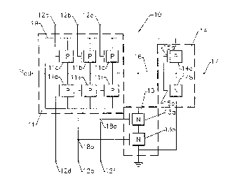
Referring now to Figure 3 a CLIP AND logic
circuit l0 according to the present invention will now
be described. The circuit of Figure 3 includes a
~driving stage iilwhich comprises a plurality of P-
~~.~i~_~~f~
-12-
channel FETs lia-11f. In Figure 3 six driving stage
FETs 11 are shown, however it will be understood by
those having skill in the art that any number of
driving stage FETs may be used. In fact, the CLIP
logic circuit 10 permits larger numbers of logical
inputs to be handled than conventional CMOS logic
gates.
Each of the driving stage FETs 11 includes a
control electrode 12a-12f for receiving logic input
signals. The driving stage FETs 11 are connected in
parallel between a first reference potential (power
supply potential Vdd) and a common output 16. As will
be described below, pairs of drains of driving stage
FETs ii may be connected to line 19 via a common
diffusion, and pairs of sources of driving stage FETs
11 may be connected to common output 16 via a common
diffusion. The driving stage FETs are preferably
enhancement type FETs having a conductive channel
region between the drain and source when the potential
at the control electrodes is near ground potential.
Still referring to Figure 3 a complementary
FET inverter 14 is serially connected between Vdd and a
second reference potential (ground), with the output 17
of the complementary inverter 14 being the output of
the logic gate l0. The input of the complementary
inverter (i.e. gates 15a and 15b) are also connected to
the common output 16. According to the preferred
embodiment of the invention, the design parameters of
the complementary inverter transistors 14a and 14b are
chosen so that a symmetric voltage transfer function is
produced.
Still referring to Figure 3 logic gate 10
also includes a gating stage 13 including a pair of
gating transistors 13a, 13b serially connected between
the common output 16 and the second reference potential
(ground). As illustrated in Figure 3, two gating
transistors are used, however any number of gating
-13-
transistors may be used. Control electrodes 18a and
18b are connected to the con.rol electrodes 12f and 12e
of transistors ilf and lie respectively. Accordingly,
gating transistors 13 are turned an when transistors
ile and ilf are turned off. It will be understood by
those having skill in the art that control electrodes
18 may be connected to any of control electrodes 12.
According to the invention, the ratio of the
channel width of the gating stage FETs 13 to the
channel width of the driving stage FETs il bears a
particular relationship for proper operation, as will
be described in detail below.
Referring now to Figure 4, a CLTP OR circuit
according to the present invention is shown. It
15 will be seen that the circuit of Figure 4 is identical
with the circuit of Figure 3 except the N and P devices
have been interchanged and ground becomes Vaa and Vaa
becomes ground. As shown in Figure 4, a single P-
channel gating stage transistor 13a is used. As is
20 well known to those having skill in the art, an N-
channel transistor is turned on with an up logic level
and off with a down logic level while a P-channel .
transistor is turned off with an up logic level and on
with a down logic level. Accordingly, the circuit of
Figure 3 provides an AND logic function and the circuit
of Figure 4 provides an OR logic function.
The design of gating transistors 13 (Figures
3 and 4) according to the invention will now be '
described. Figure 5 illustrates the drain current (Ia)
30, versus drain voltage (va) property of the gating stage
transistors 13 which is necessary for the logic
circuits of Figures 3 and 4 to function properly. As
shown in Figure 5, the drain current versus dxain
voltage of the N-channel driving stage FETs 13 and the
P-channel driving stage FETs 11 of Figure 3 is shown.
Four plots corresponding to four driving stage inputs
12 being at logic low level ("down") are shown. In
s r ~! ,i:v " )
~e
-la-
other words, the lowest current plot shown for the
driving stage corresponds to all but one driving stage
control electrode 12 at supply potential Vdd.
The saturation drain current flowing in the
gating transistor 13 must be below the saturation
current corresponding to any individual driving stage
transistor. Preferably the saturation current of any
driving stage transistor should be twice the saturation
current of the gating transistor 13. Figure 5 shows
the intersection point A where drain current in the P-
and N-channel devices are identical. The worst case
condition (i,e. all but one control electrode 12a-12t
up) must occur at a drain potential below that value
required to start switching the stage of the
complementary inverter 1~ to insure that unwanted
positive logic output does not occur when any and only
one of the gates of the driving transistors is not up.
The saturation current for P-channel devices
with the same channel dimensions as an N-channel device
is less by a factor of r~, where r~ is the ratio of
carrier mobility in an N-channel device compared to a
P-channel device. For identical saturation currents,
the channel width of the P-channel device must be r~
times the N-channel device, assuming identical channel
length. Thus, the general design criteria for the
series connected channel width Zn of the gating FETs 13
is:
Z = Isa tp Z Ln _'Sn ( 2 )
~L ~ 2
n Isa tn D
where
Z" is the channel width of the N-channel
gating FETs 13,
I""tP is the saturation current for a square
channel P-channel FET,
-15-
I'"r~ is the saturation current for a square
channel N-channel FET,
ZP is the channel width of the P-channel
driving FETs 11,
L" is the channel length of the N-channel
gating FETs 13,
L,~ is the channel length of the P-channel
driving FETs 13, and
S" is the number of N-channel gating FETs 13.
The ratio of saturation currents is defined
according to the following equation:
tl = Zee tn . ( 3 )
19a cp
This ratio is typically 2.4 for pure silicon short '
channel devices. Accordingly, if the P-channel devices
and N-channel devices of Figure 3 have the same channel
length and two N-channel devices are used as shown in
Figure 3, then Equation (2) reduces to:
Zp (4)
Thus Equation (4) is a simplified critical design
equation for proper operation of the clip AHD circuit
of Figure 3, where Sn is 2.
For the clip OR circuit of Figure 4, Equation
(2) applies, with the role o~ the N and P transistors
being reversed. Accordingly:
Z = rsatn2 ~ 'Sp (5)
"~ L ) 2
p Isatp n
which, for the simplified case reduces to:
Zv~ Znt! . (6)
2
_1~_
Figures 3 and 4 illustrate that one or more
serially connected gating transistors may be used in
the gating stage 13. The number of transistors used
depends upon the application and the logic function
required. For example, a number greater than one can
be used to control the power dissipation of the
circuits when multiple circuits are attached to a
common register. Accordingly, in Figure 4 only one
' transistor is shown and in Figure 3 two transistors are
shown.
Applying Equation (2) to a particular design
example of the clip AHD circuit of Figure 3, where all
of the devices have the same channel length and all of
the devices are fabricated in silicon integrated
circuit silicon having ~ of_about 2.4; if the driving
stage transistors 11 have a channel width of 5~ then
the gating stage FETs 13 are designed to have a width
of about 2~ according to the present invention. P-
channel FET 14a has a width of about llu and N-channel
FET 14b has a width of about 5~. Similarly, in Figure
4, the driving stage FETs il have width 5~ and the
single gating stage transistor 13a has width 6.25,
with transistor 14a having width llu and 14b having
width 5~.
Referring now to Figure 6, the results of a
computer simulation of a multiple input CLIP AND gate
of Figure 3 is illustrated. Figure 6 illustrates the
rise delay time of the gate of Figure 3 as a function
of the number of driving stage gates N,. An output
pulse only occurs at the output terminal of the
complementary inverter when and only when all gates of
the driving stage transistors ii axe up at the supply
voltage Vdd. The CLIP AND circuit is of fundamental
importance in static random access memory (SRAM) system
design where it is required to decode address registers
with a minimum delay time and minimum capacitive
loading of the register output. Decode time is
_l~_
typically 0.9 nanosecond for this circuit, as opposed
to CMOS tree logic that takes typically two nanoseconds
to decode a nine input logic function. Channel lengths
of 0. e~c are assumed.
The CLIP AND circuit of Figure 3 can be used
to efficiently decade large numbers of digital signal
inputs with far less components than conventional CMOS
technology, with a great reduction in decode time and
. with minimum capacitive loading of the driving register
output. The expression for rise delay time for the
CLIP AND logic gate of Figure 3 (graphically
illustrated in Figure 6) is given below. .
2L°Vdd CaL~ ~N9 +11 +C9 Z~ L° ( 1 +~ ) ~ ~~ )
rd I, ~ 2 Zn
nsat
Where;
Cd" - diffusion capacity F/cmz '
C,' = gate capacity F/cm2
N, = number of driving stage gates li
Z1 = Channel width of N-channel device 14b in
output inverter 14.
~
T nrat/T past
Lo = channel length
Ld = length of drain and/or source diffusion
Z" = width of N-channel device in the "AND"
gate
Figure 6 compares the effects of variations in n, with
~5 r~ of 2.5 for pure N- and P-channel silicon and also r~
of 1 when the P.-channel silicon device is nominally
doped with germanium as described below.
The rise delay time for the CLTP OR circuit
of Figure 4 is given by Equation (8)
T. = LoVdd C~L .Ng+~ +C'* Zi L (1+n) (S7
ad , a 2 2, ~ Zn °
Insa t
°
18°
The rise delay .is plotted in Figure 7 as a function of
the number of driving stage gates N,. Rise delay of
this circuit is less than the transit time through N,
CMOS devices connected in series. Accordingly, it has
been shown that CLIP logic circuits of the present
invention have very low rise delay properties even for
as many as 32 input signals.
Clocked CLlP Logic Gates
The clocked CLIP logic circuits of the
present invention will now be described. The clocked
CLIP AND logic circuit 30 of Figure 8 is identical to
the unclocked AND circuit of Figure 3 except one of the
inputs 12 is a "clock" input, for receiving a clock .
signal instead of a logic input signal. Comparing
Figures 3 to Figure 8 it may be seen that logic input
12f has been replaced by a clock input. However, it
will be understood that any other input 12 may be
replaced with the clock input, or an additional driving
stage transistor 11 may be added to accommodate the
clock input. In the clocked AND gate, the output 17 is
high when all of the gates 12a-12e are high and the
clock is high. The design considerations described
above for the gating stage 13 also apply to Figure 8.
Minimal power, typically one milliwatt, is dissipated
only during the clock time interval.
Referring now to Figure 9, a clocked CLIP OR
circuit 40 is shown. This circuit differs from the
CLIP OR circuit of Figure 4 in two respects. First,
the input control gate 18a of gating stage FET 13a is
driven by a clock input. Also, clocking FET 21 is
placed in series between second common output line 19
and ground, and the control electrode 22 is also
connected to the clock input. When a clock pulse is
applied, clocking FET 21 is turned on and gating FET 13
is turned off. If any one or more of the logic control
gates 12a-12f are up then the output of inverter 14
~~ ~~.~~3a~
-19-
rapidly rises to supply potential V~d. When the clock
pulse drops to ground potential, clocking FET 21 is
turned off and gating FET 13 is turned on. When this
occurs, the potential of the common output 16 rises
rapidly to supply potential Vdd and the output 17 of the
inverter 14 rapidly drops to ground potential.
The clocked CLIP OR circuit of Figure 9 does
not have a restriction on the channel width of the
gating FET channel. In other words, Equations (5) and
(6) do not apply to the clocked CLIP OR circuit of
Figure 9. No DC power is dissipated by this circuit.
Rise delay for this circuit is essentially the same as
that illustrated by Figure 7.
Latching Clocf~ed CLIP Logic Gates
Referring now to Figure 10, a latching
clocked CLIP AND gate 50 according to the present
invention will now be described. Latching clocked CLIP
AND gate 50 is identical to clocked AND gate 30 of
Figure 8, except that a latching stage 23 comprising a
latching FET 23a is added. The control electrode 24a
of latching FET 23a is connected to the output 17 of
the complementary inverter 14. The latching FET 23a is
connected between ground and the serially connected
gating FETs 13a and 13b respectively. In the design
example described for Figure 3, the channel dimensions
of latching FET 23 are the same as 13a or 13b. When a
single gating FET is used in gating stage l3, clocking
FET 23a is connected between ground and the common
signal line l6. Latching FAT 23 ensures that the
output 17 of complementary inverter 14 remains
unchanged during the clock period, regardless of any
change in voltage at the inputs 12a-12e.
Referring now to Figure 11, a latching
clocked CLIP OR circuit will be described. As shown in
Figure ll, the latching clock clip OR circuit differs
~from the clocked~clip.OR circuit of Figure 9 by adding
-20-
latching FET stage 23 comprising N-channel FET 23a,
which is connected between line 19 and the common
output 16. The output 17 of complementary inverter 14
is fed back to the gate 24a of the latching FET 23a.
In the design example used above, the channel width of
the clocking FET 21 is 20~ and the width of the
latching FET 23 is 5~.
In operation, a clock pulse up level connects
the gating point to ground potential via clocking stage
21, while simultaneously disconnecting the common
output 16 from the supply voltage Vdd by turning off the
gating FET 13a. During the clock pulse interval, if
any one of the driving stage transistors ila-ile is
turned on by virtue of its control 12a-12f being at
supply potential, the output 17 of the complementary
inverter 14 is switched up to supply voltage Vdd. When
this condition occurs, FETs 21 and 23 conduct, thereby
latching the complementary inverter output 17 up at the
supply potential until the end of the clock pulse.
' 20 When the clock pulse potential drops to ground
potential, gating FET 13 turns on and clocking FET 21
turns off, forcing the output of the complementary
inverter 14 to rapidly drop to. ground potential while
simultaneously turning off latching transistor 23. If
all of the driving stage resistors lia-ile are not
conditioned for conduction by virtue of their control
gates being at ground potential, the output of
complementary inverter 14 remains at ground potential
during the clock pulse.
3 o Latching CLIP Output Lo4ic Cell
Referring now to Figure 12, a latching CLIP
logic cell is shown. Any positive signal applied to
the input of this circuit is latched at the output
during the clock pulse interval regardless of whether
the input signal. drops during or after the clock pulse
interval. As shown in Figure 12A, the circuit includes
-21-
F- and N-channel driving stage FETs lia and lib
respectively, the control electrodes 12a and 12b of
which respectively are connected to the logic input. A
pair of clocking FETs 21a and 21b are connected to a
clock input. A pair of latching FETs 23a and 23b have
their control electrodes 24a and 24b connected to the
gate output 17. A complementary inverter 14 comprising
a pair of FETs 14n and 14b have their control inputs
connected to the common node 15.
As shown in Figure 12B, any positive signal
applied to the input of this circuit is latched at the
output during the clock pulse interval regardless of
whether the input signal drops during or after the
clock pulse interval.
Germanium P-Channel FETs
As heretofore described, the N- and P-channel
devices of the CLIP logic gates were conventionally
doped silicon logic gates. For a given gate area and
gate to source voltage, it is well known that silicon
P-channel devices deliver about half the saturation
current as a corresponding N-channel FET device.
According to the present invention, P-channel silicon
FETs can be improved to closely resemble N-channel FET
properties by implanting or otherwise placing germanium
ions in the channel regions of P-channel silicon
devices, with the N-channel silicon devices being free
of germanium. The germanium enhances the high field
mobility of holes within the P-channels and increases
the intrinsic carrier concentration.
Germanium also effectively reduces gate and
diffusion capacity for the P-channel devices, since
gate and diffusion capacity decrease with channel
width. Notwithstanding the decreases in gate and
diffusion capacity, the same current may be supported
as a silicon N-channel device. The Fermi potential of
the germanium compensated P-channel region is less than
CA 02101559 2000-02-16
-22-
the N-channel silicon region due to thev.~.ncrease in the
intrinsic carrier concentration for a gi'en
temperature. However, the threshold voltage for P-
channel compensated devices can be made to be equal to
5 the N-channel silicon device, particularly if Fermi
Threshold FET transistors are used. The design and
operation of the Fenai Threshold FET transistor are
described in U.S. Patent Application Serial No.
07/318,153 now U.S. Patent 4,990,974 (February 5,
10 1991); Application Serial No. 07/370,398 now U.S.
Patent No. 4,984,043 (January 8, 1991); and Application
Serial No. 07/646,829 filed January 25, 1991, all filed
by the present inventor, Albert W. Vinal, and assigned
to the assignee of the present invention.
In a preferred embodiment of the present
invention, P-channel mobility can be increased to
closely match N-channel mobility in silicon when about
20 36 atomic percent of the P-channel region is genaanium
atoms. Germanium may be introduced into a silicon
substrate in the N-channel regions using ion
implantation techniques such as those described in U.S.
Patent 4,928,156 to Alvis et al. Other well known
25 techniques may be used. As will be understood by those
having skill in the art, in order to dope the P-channel
FETs with germanium, the N-channel FETs may be covered
by an appropriate mask so that the germanium ions are
implanted only in the channel regions of the P-channel
30 FET devices, and the N-channel FET devices are free of
germanium doping.
It will also be understood by those having
skill in the art that germanium may be introduced into
P-channel FET devices of conventional MOSFET circuits
35 and in the Fermi Threshold FET of the above identified
patent application and patent. When used with the
Fermi Threshold FET, the depth of the germanium implant
-23-
should be slightly in excess of the Fermi depth Yo (as
defined in the above cited patent and patent
application) . It will also be understood by those
having skill in art that the germanium implant may
extend beyond the P-channel region to include the FET
source and drain regions of the P-channel FETs in order
to enhance the attainment of shallow or abrupt
junctions in these regions.
There are two primary effects of implanting
germanium ions in the channel region of P-channel FETs.
First, mobility a of holes within the germanium doped
silicon P-channel region increases in proportion to the
annealed percentage concentration Z of germanium in
silicon according to the following relationship:
~P = 550 + 13002. Accordingly, adding germanium to P-
channel FET devices allows for a better match between N
and P-channel device current drive capabilities for a
given gate and drain voltage.
Second, it is well known to those having
skill in the art that boron is typically present in
germanium. The presence of boron tends to make the
boron depth profile more consistent with theoretical
predictions. In other words, the boron depth profile
is more abrupt than without germanium. This allows
well controlled shallow P-type Fermi channel depths to
be achieved.
A typical dose for germanium in the P-channel
region of silicon FETs is 1E14/cm2 or greater at an
energy above 100kev. Actual implant energy must be
30~ consistent with the desired Fermi depth. This is a
moderate dose factor since the lattice constant for
silicon is 5.43A and 5.65A for germanium, and a dose of
1E14/cm2.leads to a doping spacing of about 10A.
The intrinsic carrier concentration for a
given temperature within the germanium doped silicon
channel region is greater than pure silicon and less
~than pure germanium. Intrinsic carrier concentration NL
-24-
for a given material depends on the energy gap of the
material and controls its Fermi potential. The
intrinsic carrier concentration NL for silicon and 38%
germanium doped silicon are plotted in Figures 13A and
13B as a function of centigrade temperature, where:
s (Tl 2~r~~~
N ( T) =N ~ T ~ 2 K T,rr T Trer ( 9
1 9 tlb9 CIA C
Tzer
where
T is the actual temperature in degrees
Kelvin,
T~ef is room temperature (27'C, 300K),
~~ is the substrate Fermi potential,
Ess,g is the energy gap between valence and
conduction bands at room temperature,
E~(T) is the energy gap at new temperature,
Nsubservt~ is the dopant concentration of the
substrate per cm',
K is Boltzman's Constant, and
q is the electron change.
The energy gap is defined in electron volts and for
silicon has the following temperature dependence:
E9(T) =E9(Tzee) '-~ T+1108 T0, (10)
Intrinsic carrier concentration is an
important factor in high temperature environments and
may limit the percent of germanium channel doping.
However, the advantages of doping silicon P-channel
devices with germanium outweigh the thermal penalties
when it is desired to operate complementary logic
circuits at their maximum speed while consuming the
least chip area and circuit pawer.
-25-
_Co_mmon Diffusions For Driving Stage FETs
As already described, the CLIP logic circuits
include a driving stage 11 having a plurality of
driving stage FETs which are connected between a common
output 16 and a power supply voltage (ground or Vda)~
The diffusion capacity loading of the common signal
output bus 16 is a speed limiting factor for these
circuits. Therefore, according to the invention, the
CLIP circuits illustrated by Figures 3, 4 and 8-11
l0 share diffusions that are connected to the common
signal bus. The shared diffusion reduces diffusion
capacity loading by a factor of two. The capacitive
loading effect on rise and fall delay times is thereby
minimized.
Referring now to Figures 14A and 14B, two
techniques for connecting the driving stage transistors
11 of the CLIP logic circuits between a first and
second potential and the common signal bus so as to
share diffusions connected to the output signal bus are
shown. Referring to Figure 3 and Figure 14A in
combination, the driving transistors lla-ilf are
illustrated in a portion of an integrated circuit
substrate 28. As shown, the drains 27a-2?! are
connected via line 19 to power supply voltage level Vda~
Three vertical shared source regions are found in three
common diffusion regions. The first diffusion shares
sources 26a and 26d, the second diffusion shares
sources 26b and 26e, and the third diffusion shares
. sources 26o and 26f. All of the shared sources 26a-26t ,
are connected to the common output 16. By sharing
sources 26a-26l, capacitance at the common output 16 is
reduced in half.
Figure 14B illustrates shared source
diffusion regions which are shared horizontally rather ,
than vertically. As also shown in Figure 148, drains
27 are connected to power supply Vdd via common
diffusions. It will be understood by those having
~r~~~a
y. %. t~ 4.~
-26-
skill in the art that the shared diffusion technique
may be used for any all-parallel logic circuit to
reduce diffusion capacitance by a factor of two.
In the drawings and specification, there have
been disclosed typical preferred embodiments of the
invention and, although specific terms are employed,
they are used in a generic and descriptive sense only
and not for purposes of limitation, the scope of the
invention being set forth in the following claims.