Note: Descriptions are shown in the official language in which they were submitted.
7 l3
WAVELENGTH SWITCHING LIGHT SOURCE
BACKGROUND OF THE INVENTION
The present invention relates to a wavelength switching
light source for use in optical communication systems and
the like, and more particularly to a wavelength switching
light source capable of high-speed switching of the wave-
length of output light.
Xnown examples of optical communication system re~uir-
ing high-speed switching of the wavelength of output light
include, for instance, the optical packet transfer network
described in ~Wavelength-addressed optical network using an
ATM cell-based access scheme" (by N. Shimosaka et al.),
Conference on Optical Fiber Communication/International
Conference on Integrated Optics and Optical Fiber Communica-
tion, Technical Digest Series, Volume 4 (1993), pp. 49-50.
In this system, the wavelength of the light source
should be switched and the altered wavelength should be
stabilized within the guard time left between consecutive
, .
~ packets. To meet this need, the arrangement described in
,:,
this literature uses a variable-wavelength light source
: ':' :.: '.
consisting of two semiconductor lasers and an optical switch ;~
for selectively supplying the output light of one or the
other of the twa semiconductor lasers.
Incidentally, whereas the oscillation wavelength of a
semiconductor laser varies with temperature fluctuations and
: :,: '~: .
2 ~ ~
accordingly these temperature fluctuations should be compen-
sated for, the variable-wavelength light source described in
this literature requires either a temperature compensation
circuit for each semiconductor laser or a constant tempera-
ture device accommodating a plurality of semiconductor la-
sers, and entails the problem that the dimensions of the
variable-wavelength light source would increase with the
number of wavelengths used.
SUMMARY OF THE INVENTION
The object of the present invention is to provide a
variable-wavelength light source whose dimensions will hard-
ly enlarge even if a wavelength range used increases.
According to the invention, there is provided a wave-
length switching light source for varying the wavelength of
the output light in accordance with a wavelength designating
signal and a wavelength switching signal, both supplied from
outside, comprising~
a variable-wavelength light source whose oscillating
wavelength varies in accordance with a wavelength control
signal;
a light brancher for branching the output light of said
variable-length light source into two beams, of which one is
supplied externally as an output light and the other is
brought to incidence on an optical resonator; :~
said optical resonator ha~ing a periodic wavelength
,, ~ .
2 ~ ~
2 7 ~
transmitting characteristic;
an optical detector for detecting the power of the
output light of said optical resonator and outputting a
value corresponding to this power;
Means for outputting a first wavelength
control signal which is proportional to the balance of the ~'
subtraction of said optical detector output value from a
fixed value;
wavelength control means for outputting a second wave-
length control signal re~uired for oscillating said optical-
wavelength light source at a designated wavelength in accor-
dance with said wavelength designation signal and said wave- ~
length switching signal; and ~;
adder means for adding said first wavelength control
signal and said second wavelength control signal to output
: : :
said wavelength control signal.
BRIEF DESCRIPTION OF THE DRAWINGS :
FIG. 1 is a block diagram illustrating a preferred
embodiment of the present invention;
FIG. 2 is a diagram illustrating the wavelength trans-
mitting characteristic of the optical resonator of FIG. 1; :
FIG. 3 is a block diagram illustrating the configura-
tion of the wavelength control circuit 108 of FIG. 1;
FIG. 4 is a circuit diagram illustrating the configura~
tion of the constant current circuit of FIG. 2; and
3 ;~
7 0
FIG. 5 iS a block diagram illustrating another possible
configuration of the waveleng-th control circuit 108.
DETAILED DESCRIPTION OF THE PREFERRED EMBODIMENT
A preferred embodiment of the present invention will be
described below with reference to FIG. 1. As shown in FIG.
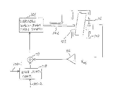
1, the preferred embodiment of the invention consists of a
variable-wavelength light source 101; a light brancher 102
for branching the output light of the variable-wavelength
light source into two beams, of which one is supplied exter-
nally as an output light; an optical resonator 103, to which
the other of the outputs of the light brancher 102 is 9up-
plied, for supplying transmitted light; a temperature con-
trol device 104 for accommodating the optical resonator 103; ~:~
an optical detector 105 for outputting a voltage 1ndicating
the power of the transmitted light; an operational ampli~ier 106 ~or
outputting, as a first wavelength control current, a current
which is proportional to the balance of the subtraction of
. . ..
: the output of the optical detector from a fixed reference
voltage; a wavelength control circuit 108 for outputting a
second wavelength control current in accordance with a wave-
:,
length switching signal 100-1 and a wavelength designation
~ signal 100-2, both supplied from outside; and an adder 107 ;~
: for adding the first wavelength control cuxrent signal and
the second wavelength control signal to supply the result of
addition to the variable-wavelength light source 101 as a
CA 02102270 1998-12-02
wavelength control current.
The variable-wavelength light source 101 outputs
oscillating light of a wavelength corresponding to the
wavelength control current supplied from the adder 107. As
this variable-wavelength light source can be used, for
example, a DFB semiconductor laser. As is well known to those
skilled in the art, a DFB semiconductor laser has such a
property that its oscillating wavelength lengthens with an
increase in injection current.
The oscillating light from the variable-wavelength
light source 101 is branched by the light brancher 102 into
two beams, of which one is emitted outside as output light and
the other is brought to incidence on the optical resonator
103.
As the optical resonator 103 can be used a Fabri-
Perot etalon, for instance, which shows a periodic wavelength
transmission characteristic as shown in FIG. 2. In FIG. 2,
the horizontal axis represents the wavelength of the input
light and the vertical axis, the relative volume of the
detection voltage at the time of detecting the transmitted
light power with an optical detector. As this optical
resonator 103 can also be used a Machzender type optical
resonator. This optical resonator 103 is housed in the
temperature control device 104 and kept at a constant
temperature. As is evident from FIG. 122, when the wavelength
of
66446-569
2~0227a
the input light varies, the output voltage of the optical
detector substantially varies in the rising and falling
parts of the transmission characteristic. The intensity of
this transmitted light is converted into a voltage by the
optical detector 105.
The output voltage of the optical detector 105 is
supplied to the negative side input terminal of the oper-
ational amplifier 106. On the other hand, the positive side
input terminal of the operational amplifier is supplied with
a fixed reference voltage. This reference voltage is set at
a level corresponding to the mid-point between the peak
level and the bottom level of the input wavelength-optical
detector output voltage characteristic shown in FIG. 2. As ~;
shown in FIG. 2, wavelengths Al, ~2~ ~3~ ~4,---, correspond~
ing to the intersection points between this reference volt~
age and the rising parts of the wavelength-output voltage
characteristic are the oscillating wavelengths at which the
variable-wavelength light source 101 is to be set. The
operational amplifier 106 supplies, as the first wavelength
control current, a current of a value proportional to the
balance of the subtraction of the optical detector output
voltage from the reference voltage. This first wavelength
control current is supplied to one of the input terminals of
the adder 107.
Here is considered a case in which the oscillating
~22 70
wavelength of the variable~wavelength light source 101 is
set at the wavelength ~2 in FIG. 2, when a current value
i(~2) to cause the variable wavelength light source 101 to
oscillate at the wavelength ~2 is supplied, as the second
wavelength control current, from the wavelength control
circuit 108 to a second input terminal of -the adder 107.
Thu~ the wavelength control circuit 108 outputs, as the
s cond wavelength control current, a current of the value at -~
which the variable-wavelength light source 1 oscillates at
the wavelength ~2 when the first wavelength control current
is made zero.
If, in this case, the oscillating wavelength of the
variable-wavelength light source 101 is lengthened by a tempe-
rature variation, the output voltage of the optlcal detector
will increase as is obvious from FIG. 2, and a negative
current is supplied from the operational amplifier 106. As
a result, the wavelength control current, which is the
output of the adder 107, will decrease, and the oscillating
wavelength of the variable-wavelength light source 101 will
~ , ~.. -: -; :
shorten. Conversely, iE the oscillating wavelength of the ~ ~ ~
variable-wavelength light source 101 shortens, the output ~ii i~'
voltage of the optical detector 105 will decrease, the
wavelength control current will increase, and the oscillat-
: ::
ing wavelength of the variable-wavelength light source 101
willlengthen~In this manner, th~ oscillating w-velength of
: :::
~ '
i- x ~ : .: : :
~22~
the variablei-light source 101 is stabilized at ~2'
The wavelength control circuit 108 will be described
with reference to FIG. 3 as well. As shown in FIG. 3, the
wavelength control circuit 108 consists of two current
sources 202 and 203, of which one supplies the second wave-
length control current when the other is in a hot stand-by
state, and a control circuit 201. The control circuit 201,
in accordance with the wavelength switching signal 100-1
supplied from outside, switches via signal lines 206 and 207
the current source in the hot stand-by state to an active
state and the other current source, which is in the active
state, to the hot stand-by state. The control circuit 201,
in accordance with the wavelength designation signal 100-2
supplied from outside, further supplies the current source
in the hot stand-by state with a bias voltage required for
oscillating the variable wavelength light source 101 at the ~ ~ ;
designated wavelength. -
It is now supposed that the current source 202 is in an ~ -
active state and the current source 203, in a hot stand-by
state. Then the current source 202 supplies the adder 107
with an already set constant current, for instance i(~2)
mentioned above. And when a wavelength designation signal
indicating the wavelength ~2 is supplied via a signal line
100-2, the control circuit 201 supplies the current source
203 in the hot stand-by state via a signal line 205 with a
52 ril ~
bias voltage to cause the current i(A2), which is required
for having the variable-wavelength light source 101 oscil-
late at the wavelength ~2' corresponding to this wavelength
designation signal, to be outputted. After that, when the
wavelength switching signal 100-1 is supplied to the control
circuit 201, the current source 202 shifts to the hot stand-
by state, and the current source 203 takes on the active ~:
state to supply the current i(~2) to the adder 107.
Next will be described the configuration and operations
of the constant current sources 202 and 203 with reference
.
to FIG. 4. Since the two current sources are of the same ::~
configuration, only the current source 202 will be described. :
When the current source 202 of FIG. 4 is switched fromthe hot stand-by state to the active state, a signal line
204 supplies a signal which shifts from a low to a high
level, and this signal is supplied via a terminal A and a
resistor R1 to the base terminal of a switching transistor ~;
Q1. On the other hand, the base terminal of another switch-
ing transistor Q2 is supplied via an inverter 401 and a
resistor R2 with a signal which shifts from a high to a low
level. As a result, the transistor Ql is turned on, and the
transistor Q2, turned off. By that time, at the base termi-
nal of still another Q3 will have been set a bias voltage Vc
corresponding to the desired oscillating wavelength, this
bias voltage having been supplied when the constant current
: :
9 : .
:
~1~227~
source 202 was in the hot stand-by state. To a signal line
208-1 is outputted a current corresponding to the desired
oscillating wavelength via the transistors Ql and Q3, and
this current is supplied to the adder 107 of FIG. 1.
Next, when the signal from the signal line 204 shi.fts
from a high to a low level and the current source 202 takes ~ :
on the hot stand-by state, the transistor Q1 is turned off
and the transistor Q2, turned on. Then, as the current
flows via the transistors Q2 and Q3 between power sources
~VDD and +Vss, the output current of the current source 202
is not supplied to the adder 107 of FIG. 1 and, as stated
already, a bias voltage corresponding to the wavelength to
be used when this current source 202 takes on an active
state next time is set at the base terminal of the transis~
tor Q3 via the signal line 206.
In this way, this preferred embodiment of the present
invention requires no more than one optical resonator and
one comparator for its temperature dependence stabilizing
mechanism even if a Iarge wavelength range is used,
resulting in the advantage that the hardware dimensions will
not enlarge.
FIG. 5 illustrates a second conceivable configuration
of the wavelength control circuit 108. What di~ferentiate
the configuration of FIG. 5 from that of FIG. 3 are, first,
that a constant current source 204, which outputs a fixed
' .
":,~ ",;~"~ ""~" ,,~, ~'"~ ," ',"' ~ "~
~ ~2~7~
current value all the time, is newly provided here and,
second, that the output curren-t values of curren-t sources
202a and 203a of FIG. 5 are smaller than those of the cur-
rent sources 202 and 203 of FIG. 3 by the output current
value of the constant curren-t source 204. When wavelengths
2~ ~3~ Of FIG. 2 are to be used as the oscil-
lating wavelengths of the variable-wavelength light source,
the wavelength control circuit of FIG. 3 requires not only
the current source in the active state but also that in the
hot stand-by state to supply at least a current correspond-
ing to the wavelength ~1 By contra~t, in the wavelength
control circuit o~ FIG. 5, the current value corresponding
to the wavelength ~1 is supplied by the constant current
source 204, and the current sources 202a and 203a need to
supply nothing more than the current value corresponding to
the dif~erence between the desired wavelength and the wave~
length ~1~ so that this circuit consumes less power than
that of FIG. 3.
::
, "~.:: , : ' . . ~ . ~ ,. : .