Note: Descriptions are shown in the official language in which they were submitted.
2102~2~
The present invention relates to an accumulator
for use in updating coefficients, and more
particularly to a two stage accumulator for updating
the coefficients of an adaptive equalizer or the
like.
Digital data, for example digitized video for
~.0 use in broadcasting high definition television
(HDTV) signals, can be transmitted over terrestrial
very high frequency (VHF) or ultra high frequency
(UHF) analog channels for communication to end
users. Analog channels deliver corrupted and
transformed versions of their input waveforms.
Corruption of the waveform, usually statistical, may
be additive and/or multiplicative, because of
possible background thermal noise, impulse noise,
and fades. Transformations performed by the channel
are frequency translation, nonlinear or harmonic
distortion, and time dispersion.
In order to communicate digital data via an
analog channel, the data is modulated using, for
example, a form of pulse amplitude modulation (PAM).
Typically, quadrature amplitude modulation (QAM) is
~1~2328
used to increase the amount of data that can be
transmitted within an available channel bandwidth.
QAM is a form of PAM in which a plurality, such as
sixteen or thirty-two, bits of information are
transmitted together in a pattern referred to as a
"constellation".
In pulse amplitude modulation, each signal is a
pulse whose amplitude level is determined by a
transmitted symbol. In 16-QAM, symbol amplitudes of
-3, -1, 1 and 3 in each quadrature channel are
typically used. In bandwidth efficient digital
communication systems, the effect of each symbol
transmitted over a time-dispersive channel extends
beyond the time interval used to represent that
symbol. The distortion caused by the resulting
overlap of received symbols is called intersymbol
interference (ISI). This distortion has been one of
the major obstacles to reliable high speed data
transmission over low background noise channels of
limited bandwidth. A device known as an "equalizer"
is used to deal with the ISI problem.
In order to reduce the intersymbol interference
introduced by a communication channel, rather
precise equalization is required. Furthermore, the
channel characteristics are typically not known
beforehand. Thus, it is common to design and use a
compromise (or a statistical) equalizer that
compensates for the average of the range of expected
channel amplitude and delay characteristics. A
CA 02102328 2002-04-19
3
1
least mean square (LMS) error adaptive filtering
scheme has been in common use as an adaptive
equalization algorithm for many years. This
algorithm is described ire B. Widrow and M. E. Hoff,
Jr., "Adaptive Switching Circuits" in IRE Wescon
Conv. Rec., Part 4, pp..96-104, Aug. 1960. The use '
of the hMS algorithm in an adaptive equalizer to
reduce intersymbol interference is discussed in S. ,
U. H. Qureshi, "Adaptive Equalization", Proc..IEEE,
Vol. 73, No. 9, pp. 1349-1387, Septemper 16.87.._
Commonly assigned U.S. Patent No. 5,243,624
discloses a method and apparatus for updating
coefficients in a complex adaptive equalizer.
Specifically, convergence of a complex adaptive
equalizer used.in digital communications is
substantially improved by updating all coefficients
of the equalizer during each filter clock cycle. A
plurality of successive delay stages are coupled to
provide a plurality of sets of delayed signal data
from an input signal. Each set of delayed data is
multiplied by an error signal to provide a plurality
of products. Each product is concurrently updated
with previous product data to provide a plurality of
sets of updated coefficients. The updated
coefficient sets are selectively input to an
equalizer filter stage.
In a specific embodiment illustrated in the
aforementioned copending patent application, a
4
plurality of parallel processing paths are used,
each to update one of the products. Each of the
parallel processing paths includes an adder having a
first input for receiving one of the plurality of
products, a second input and an output. A delay
circuit is coupled to receive product data from the
adder output and to feed delayed product data back
to the second adder input. The parallel processing
paths can further include means for truncating
and/or adjusting the gain of the updated.
coefficients output from the adder. Sets of updated
coefficients from the various parallel paths are
multiplexed to provide a clocked stream of
coefficient sets for input to the equalizer filter
stage.
A disadvantage to using adders as accumulators
in the implementation disclosed in the
aforementioned copending patent application is that
such devices require an inordinate amount of space
in a very large scale integration (VLSI) integrated
circuit. Thus, the use of a conventional adder and
delay stage as an accumulator increases the cast and
may decrease the performance of an adaptive
equalizer implementation.
Tt would be advantageous to provide an improved
implementation for an accumulator that can be used
in connection with an adaptive equalizer or the
like. Such an implementation should avoid the need
for a long bit adder which requires substantial
~1Q2~;~
hardware and may slow down the equalizer processing
speed. It would be further advantageous to provide
such an accumulator implementation which will
improve the convergence of the coefficients by
5 dynamically maintaining limits on the coefficient
magnitudes.
The present invention provides a two stage
accumulator enjoying the aforementioned advantages.
6 ~~~23~8
In accordance with the present invention, a two
stage accumulator is provided for use in updating
coefficients. A first stage is coupled to receive
an error word. The first stage outputs sign and
carry bits resulting from the addition of the error
word and an N-bit least significant bit (LSB)
portion of a larger M-bit coefficient. A second
stage is responsive to the sign and carry bits from
the first stage for updating the (M-N) most
significant bits ('MSB's) of the M-bit coefficient.
Means are provided for cyclically providing new
error words to the first stage during successive
coefficient update cycles.
In an illustrated embodiment, the new error
words are derived from at least a portion of an M-
bit coefficient that was updated during a previous
coefficient update cycle. The first stage adds the
new error word received during a coefficient update
cycle to the N least significant bits of the M-bit
coefficient from the previous coefficient update
cycle to provide the sign and carry bits. The
second stage is responsive to the sign and carry
bits output from the first stage during each cycle
to update the (M-N) most significant bits of the M-
bit coefficient from the previous coefficient update
cycle.
210328
Tn the illustrated embodiment, the error word
is an N-bit word. The first stage comprises an N-
bit twos complement adder for adding th'e error word
and the N-bit LSB portion to produce a sign bit, a
carry bit, and an N-bit sum. The sign and carry bit
are delayed for input to the second stage during a
subsequent coefficient update cycle. The N-bit sum
is also delayed for input to the adder as the N-bit
LSB portion during the subsequent coefficient update
cycle.
The second stage can comprise an up/down
counter for selectively incrementing or decrementing
the (M-N) most significant bits depending on the
state of the sign and carry bits during a current
coefficient update cycle. In a preferred
embodiment, means are provided for inhibiting the
incrementing of the (M-N) most significant bits if
such incrementing wauld cause the {M-N) MSB's to
exceed an upper boundary. Likewise, means are
2o provided fox inhibiting the decrementing of the
(M-N) most significant bits if the decrementing
would cause the (M-N) MSB's to drop below a lower
boundary. Leakage function means are provided to
cause the up/down counter to periodically skip
incrementing and decrementing cycles. In an
illustrated embodiment, first leakage function means
are responsive to the number of incrementing cycles
of the up/down counter over time. Second leakage
~~~~:zs
function means are responsive to the number of
decrementing cycles aver time.
Means are also provided for preloading the
up/down counter and the incrementing and
decrementing inhibiting means with initialization
data for at least a portion of the (M-N) most
significant bits of the M-bit coefficient during an
accumulator initialization cycle. Preloading of the
incrementing and decrementing inhibiting means
provides stability for an adaptive equalizer which
uses the accumulator of the present invention.
Preloading of the up/down counter is provided to
deal with the echo problem in communication system
implementations.
In a more specific embodiment, the present
invention provides a two stage accumulator for use
in updating coefficients in which the first stage
includes an N-bit twos complement adder and the
second stage includes an up/down counter. The N-bit
twos complement adder has a first input coupled to
receive an N-bit error word and a second input
coupled to receive a previous N-bit sum from the
adder. The adder also has a first output for
outputting a new N-bit sum resulting from the
addition of the error ward and the previous sum, and
a second output for outputting sign and carry bits
resulting from the addition. The sums represent the
N-bit least significant bit portions of an M-bit
coefficient being cyclically updated. The up/down
2~Q2~~~
9
counter means in the second stage are responsive to
the sign and carry bits from the second output of
the adder. The up/down counter means update the
(M-N) most significant bits of the M-bit
coefficient. New error words are cyclically
provided to the first stage adder for updating the
M-bit coefficient.
The up/down counter means of the second stage
selectively increment or decrement the (M-N) most
significant bits, depending on the state of the sign
and carry bits during a current coefficient update
cycle. Means can be provided for inhibiting the
incrementing and decrementing of the (M-N) most
significant bits to prevent them from exceeding
predetermined boundaries.
First delay means are coupled to the first
output of the adder for delaying the new N-bit sum
for input to the second input of the adder during a
subsequent cycle. Second delay means are coupled to
the second output of the adder for delaying the sign
and carry bits for use in controlling the up/down
counter during the subsequent cycle.
4
1~
In the drawings,
Figure 1 is a block diagram of a typical
transmission system illustrating the location of an
adaptive equalizer;
Figure 2 is a block diagram of a multi-tap
complex adaptive equalizer using cascaded
components;
Figure 3 is a block diagram of a coefficient
update computation circuit that uses a Long bit
adder as an accumulator in each of a plurality of
parallel processing paths;
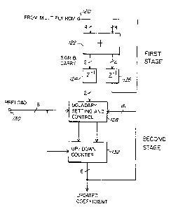
Figure 4 is a block diagram of a two stage
accumulator in accordance with the present invention
that can replace the accumulators illustrated in
Figure 3; and
Figure 5 is a flow chart illustrating the
operation of the two stage accumulator of Figure 4.
11
In the transmission system illustrated in
Figure 1, a signal to be transmitted is input to a
transmitter 12 via an input terminal 10. The signal
contains digital data, modulated on an analog
carrier using, for example, well known QAM
techniques. The QAM modulated data is a complex
signal that includes real components I and imaginary
components Q. Transmitter 12 is a conventional
device, such as a well known VHF or UHF transmitter.
The transmitted signal is communicated via a
channel 14, such as a terrestrial VHF or UHF
communications channel, to a receiver that contains
a quadrature demodulator 16 for the QAM data.
Quadrature demodulator 16 is a conventional
component that extracts the I and Q components of
the received data for input to a complex adaptive
equalizer 18. Adaptive equalizers, per se, are well
known in the art. The present invention provides an
accumulator that can be used, for example, in an
adaptive equalizer.
As illustrated in Figure 1, the received
channel data input to complex adaptive equalizer 18
is unequalized, and suffers from the intersymbol
interference caused by the amplitude and/or delay
distortion introduced by communication channel 14.
Adaptive equalizer l8 compensates for this
distortion, and outputs equalized channel data Iequ
12
and Q~~~. The equalized channel data is input to a
conventional decoder 20 to retrieve the transmitted
information data, which can comprise, for example,
HDTV video information.
Figure 2 illustrates an embodiment of complex
adaptive equalizer 18 in greater detail.
Unequalized channel data from the quadrature
demodulator is input at terminals 30, 32
respectively. Terminal 30 receives the real (I)
demodulated channel data and terminal 32 receives
the imaginary (Q) demodulated channel data. Each of
the demodulated I and Q signals comprise m-bit bytes
that are input both to a first stage 34 of N-tap
finite impulse response (FIR) filters and a q-bit
quantizer 38. Quantizer 38 quantizes each m-bit
byte into a smaller byte for input to an N-
coefficients update computation circuit 36.
As shown in Figure 2, equalizer 18 comprises M
sets or stages, each containing an N-tap FIR filter
circuit and an N-coefficients update computation
circuit. After the last (Mth) stage, the outputs
from the last N-tap FIR filter circuit are combined
in adders 40, 42 to provide the real equalized
channel data I and the imaginary equalized channel
data Q. The equalized I and Q data is also input to
an error signal generator 44, which outputs an error
signal that is fed back to each of the update
computation circuits 36 to 36M. In a preferred
embodiment, error signal generator 44 comprises~a
iV
13
programmable read only memory (PROM) that outputs a
precalculated stored error value in response to the
Q and I data that is used to address the PROM. The
stored error values have been previously computed
using the well known LMS algorithm.
Figure 3 illustrates a 64 tap complex
coefficient update computation circuit 36 in which
the accumulator of the present invention can be
utilized. Two-bit quantized unequalized complex
data (real and imaginary) is input at terminals 90
(real) and 92 (imaginary). Similarly, the two-bit
quantized real and imaginary components of a complex
error signal are input at terminals 96, 98
respectively. Sixty-four cascaded delay stages 94
receive the real and imaginary data for input, alang
with the error signals, as addresses to a multiply
read-only memory (ROM) that obtains the product of
each data component with each error component for
input to an accumulator and gain adjust circuit
associated with the particular delay stage from
which the data was output. Circuit 102a is an
example of one of the accumulator and gain adjust
circuits.
As can be seen in Figure 3, each accumulator
and gain adjust circuit 102a to 102n includes a 20-
bit accumulator 104 that sums the respective product
from multiply ROM 100 with a delayed product output
from delay circuit 106. Delay circuit 106 outputs
20-bit delayed coefficients. The 20-bit accumulator
2102328
14
is used to update the coefficients. After
accumulation, the coefficients are truncated and
gain adjusted in a conventional truncation and gain
adjust circuit 108. The gain adjustment adjusts the
magnitude of the coefficients. A multiplexer 110
receives all of the coefficients from each stage,
multiplexes them together, and selects one set for
output each clock cycle. A clock input 112 is
provided to input the clock signal to multiplexer
l0 110.
As noted above, a 20-bit accumulator such as
accumulator 104 illustrated in Figure 3 is costly to
implement in an integrated circuit due to the amount
of space the accumulator takes up. The present
invention overcomes this problem by providing a two
stage accumulator as illustrated in Figure 4.
The embodiment illustrated in Figure 4 is used
to update coefficients having a length of 20 bits.
It should be appreciated that the specific
embodiment illustrated is only an example, and the
present invention can be used to implement a two
stage accumulator for coefficients of any length.
In the illustrated embodiment, a first stage
comprising adder 222 and delay circuits 124, 126
comprise the first stage of the accumulator. The
first stage processes the least significant four
bits of each 20-bit coefficient. The second stage
of the accumulator includes a boundary setting and
control circuit 128 and up/down counter 132. The
15~~~~~~
second stage processes the remaining 16 bits of each
coefficient.
First stage adder 122 receives the current
error and delayed data product from multiply ROM 100
(Figure 3) via terminal 120. This 4-bit error word
is added to the prior 4-bit sum from adder 122,
which is delayed by delay circuit 126. The addition
produces six bits. Four of the bits comprise the
sum resulting from the addition of the error word
and the previous sum, and are output from a first
output of adder 122 to delay stage 126. The other
two bits are a sign and carry bit that are output
from a second output of adder 122, to a delay stage
124. delay stages 124 and 126 are conventional
circuits that each provide a delay equal to one
coefficient update cycle of the accumulator.
In the illustrated embodiment, adder 122 is a
conventional twos complement adder. The four bits
comprising the sum output from the adder correspond
to the four least significant bits of the 20-bit
coefficient. The 4-bit error word input to terminal
120 comprises, as its most significant bit, a sign
bit. The remaining 3 bits represent the error
magnitude. Ultimately, the sign bit is extended to
the most significant bit of the full 20-bit
coefficient.
The sign and carry bits output from delay stage
124 are input to the second stage of the accumulator
via boundary setting and control circuit 128. This
2~p2328
16
circuit comprises a comparator that determines
whether the current magnitude of the sixteen most
significant bits of the coefficient is within a
predetermined range. If so, the sign and carry bits
will determine whether the up/down counter 132
should be incremented, decremented, or maintained at
its current value according to the following table:
Sian Carry Up/Down Counter
0 0 ..... no change
0 1 ..... count up 1
1 0 ..... count down 1
1 1 ..... no change
As can be seen, if the sign bit is a 0 and the carry
bit is a 1, boundary setting and control circuit 128
will cause up/down counter 132 to count up by 1. If
the sign bit is a 1 and the carry bit is.a 0, the
up/down counter 132 will be actuated to count down
by 1. If the sign and carry bits are the same,
up/down counter 132 will remain at its current
value,
The action of up/down counter 132 will update
the sixteen most significant bits of the 20-bit
coefficient. The current updated coefficient is fed
back from the output of up/down counter 132 to the
input of boundary setting and control circuit 128
for a determination, during the next coefficient
update cycle, as to whether the coefficient has
exceeded its upper permitted bound or dropped below
its lower permitted bound. If this occurs, circuit
1~ 2~ 02328
128 will not actuate up/down counter 132 to
increment above or decrement below the boundary. By
limiting the range of the coefficient in this
manner, the coefficient will not grow unbounded.
Another function of boundary setting and
control circuit 128 is to provide a "leakage
function." During the operation of an adaptive
equalizer, the coefficient update routine will
eventually reach a steady state. However, if the
steady state is reached too quickly, the
equalization may not be stable. Therefore, it is
advantageous to introduce "leakage" to effectively
slow down the update of the coefficient, thereby
stabilizing the adaptive equalizer.
The present invention enables a leakage
function to be implemented in a very straightforward
manner. Specifically, boundary setting and control
circuit 128 can include a first counter to keep
track of the number of increments provided by
up/down counter 132 and a second counter to keep
track of the number of decrements provided by the
counter. After the first counter counts X
increments, the next increment that would otherwise
be effected by up/down counter 132 will be skipped.
Similarly, after the second.counter counts Y
decrements, the next decrement that would otherwise
be effected by the up/down counter will be skipped.
After an increment or decrement is skipped, the
respective first or second counter is reset. Thus,
18 ~1~2~~~
an increment will be skipped every X times and a
' decrement will be skipped every Y times. X and Y
can each be any number, depending on the specific
implementation, and can be the same or different.
By periodically skipping increments and
decrements as indicated above, the updating of the
coefficient will be slowed dawn, since certain
update cycles will be wasted. As noted above, this
procedure will prevent the coefficient from reaching
a steady state value too quickly, thereby
stabilizing the equalizer.
As indicated in Figure 4, boundary setting and
control circuit 128 anti up/down counter 132 are
preloaded via terminal 130 with initialization data
for at least a portion of the sixteen most
significant bits of the 20-bit coefficient.
Preloading of the boundary setting and control
circuit provides stability for the coefficient
update process. Preloading of the up/down counter
facilitates proper echo cancellation when the
accumulator is used in an adaptive equalizer. The
problem of echo cancellation in an adaptive
equalizer is discussed in the article to S. U. H.
Qureshi referred to above.
When the two stage accumulator of the present
invention is used in the adaptive equalizer
illustrated .in Figure 3, the updated coefficient
output from up/down counter 132 during each
coefficient update cycle is input to truncation and
~~~~328
19
gain adjust circuit 108. Since the updated
coefficient is truncated anyway, only the sixteen
MSB's of the 20-bit coefficient need to be passed on
to the truncation stage. However, in an embodiment
where the full 20-bit coefficient is necessary for
further processing, the four bits output from delay
stage 126 of the first accumulator stage can be
appended as LSB's to the 16 bits output from up/down
counter 132 to form the full 20-bit coefficient.
Figure 5 is a flow chart illustrating the
operation of the two stage accumulator of the
present invention. As indicated at box 140,
processing commences with the input of an N-bit
error product to the adder. With reference to
Figure 4, this corresponds to the input of the error
word at terminal 120. At box 142, the N-bit error
product is added to the accumulated value of the
four LSB's output from delay stage 126.
The sign and carry bits output from the first
stage of the accumulator are tested at box 144 to
determine if the sign is a 0 and the carry is a 1.
Tf so, the up/down counter will be incremented if
two additional tests are met. First, a
determination is made at box 148 as to whether~the M
25, (e. g., 16) most significant bits of the coefficient
are below their upper boundary limit. If so, a
determination is made at box 149 as to whether the
current coefficient update cycle is a leakage cycle,
i.e., a cycle during which the next increment o.f the
20
up/down counter is to be skipped. If this is not
the case, the up/down counter is incremented at box
152. If either of the tests at boxes 148 or 149 are
not met, the counter is not incremented.
If the test performed by box 144 is not met,
box 146 will make a determination as to whether the
sign bit is a 1 and the carry bit is a 0. If so,
box 150 tests the M most significant bits to
determine if they are greater than the lower
boundary limit. If so, box 151 determines whether
the current coefficient update cycle is one where
the decrementing of the up/down counter is to be
skipped. If not, the up/down counter is decremented
at box 154. Otherwise, the up/down counter will not
be decremented.
After the appropriate action, if any, has been
taken by the up/down counter, the updated
coefficient will be output as indicated at box 156.
The procedure then returns to box 140, where the
next coefficient update cycle is commenced with the
input of a new N-bit error product to the adder.
It should now be appreciated that the present
invention separates an M-bit coefficient update
circuit into a two-level function. The first level
is an N-bit adder'which implements the update of the'
total dynamic range of an error signal. The error
signal is derived from at least a portion of the
coefficient updated during a previous coefficient
update cycle. The remaining (M-N) most significant
21
bits of the M-bit coefficient are updated using only
the sign and carry bits from the first level. The
sign and carry bits provide information as to
whether the remaining bits should be incremented,
decremented, or left at their current value. They
can also be used for leakage control. In an
illustrated embodiment, leakage control is provided
using separate counters that keep track of how many
times the coefficient has been incremented and how
many times it has been decremented. Based on these
counts, the incrementing and decrementing functions
will periodically be skipped. After the skipping of
a cycle, the respective increment or decrement
counter is reset.
Although the invention has been described in
connection with a specific embodiment thereof, those
skilled in the art will appreciate that numerous
adaptations and modifications may be made thereto
without departing from the spirit and scope of the
invention as set forth in the claims.