Note: Descriptions are shown in the official language in which they were submitted.
2 1 02661
DIFFERENTIAL AMPLIFIER CIRCUIT USING QUADRITAIL CIRCUIT
BACKGROUND OF THE INVENTION
1. Field of the Invention
The present invention relates to a differential amplifier
circuit using a quadritail circuit, and more particularly to a
differential amplifier circuit to be formed on Complementary
Metal Oxide Semiconductor (CMOS) integrated circuits, which has
an improved transconductance linearity.
2. Description of the Prior Art
In general, with a differential amplifier circuit formed on
CMOS integrated circuits, its input voltage range is determined
by the transconductance of the differential circuit formed at
the input end of the differential amplifier circuit.
Therefore, the differential circuit is required to have a
transconductance with good linearity.
Fig. 1 shows a conventional differential amplifier circuit
whose transconductance is good in linearity, which is disclosed
by A. Nedungadi and T. R. Viswanathan in "IEEE TRANSACTIONS ON
CIRCUITS AND SYSTEMS", Vol. CAS-31, No.10, pp. 891-894, October
1984, entitled "Design of Linear CMOS transconductance
Elements". Fig. 2 shows the squaring circuit used in the
21026~1
differential amplifier circuit. It seems that there are some
mistakes about the operation analysis in the document, so that
the corrected operation analysis of the circuit is described
below.
In Figs. 1 and 2, N-channel MOS transistors M21 and M22
compose a first pair and N-channel MOS transistors M23 and M24
compose a second pair. The first pair is driven by a constant
current source 21 which is connected to the common-connected
sources of the transistors M21 and M22 and generates a constant
current (n+l)I. The second pair is driven by a constant current
source 22 which is connected to the common-connected sources of
the transistors M23 and M24 and generates a constant current
(n+l)I.
The transconductance parameters of the transistors M21 and
M22 are k and those of the transistors M23 and M24 are n times
as much as k, or nk. The MOS transistor with the
transconductance parameter nk is generally realized by n in
number of the unit transistors with the transconductance
parameter k which are connected in parallel.
N-channel MOS transistors M26 and M27 whose sources are
connected in common at a point D compose a differential pair,
which is driven by a constant current source 23. The current
21026~
source 23 is connected to the differential pair at the point D
and generates a constant current aI. The transconductance
parameters of the transistors M26 and M27 are k.
The drains of the transistors M21 and M22 are connected in
common at a point C, and between the drains thus common-
connected and a voltage source (voltage: V), there is provided
with a constant current source 24 which generates a constant
current aI. An N-channel MOS transistor 25 whose drain and gate
is connected to each other is provided between the points C and
D. The transistor M25 serves as a current level shifter for
shifting the current level at the point C to that at the point
The gates of the transistors M26, M21 and M23 are connected
in common to be applied with a first input voltage Vl. The
gates of the transistors M27, M22 and M24 are connected in
common to be applied with a second input voltage V2.
P-channel MOS transistors M28 and M29 compose a current
mirror circuit serving as an active load of the differential
amplifier circuit. An output current i of the differential
amplifier circuit is derived from the drain of the transistor
M29.
Next, the operation of the conventional differential
210~6~
amplifier circuit will be explained below.
The transconductance parameter k is expressed as
k = (1/2)(W/L)~Co%, where ~ is the effective surface carrier
mobility, COx is a gate-oxide capacity per unit area, W is a gate
width and L is a gate length of each of the transistors.
Assuming that all the MOS transistors are operating in their
saturation regions, the drain current ID f each transistor is
expressed by the following equation (1), where VGS is the gate-
to-source voltage and V~ is the threshold voltage of each
transistor.
ID = k(VGS TH) ( 1 )
Consider now a source-coupled N-channel differential pair
biased by a current sink 2I, the differential input voltage (V1
- V2) is expressed as v and the drain current ID is expressed as
I + i, where I is a direct current component and i is a signal
component varying in accordance with the differential input
voltage v. Assuming that the transistors is matched in
characteristic to each other, the large signal v-i
characteristic (input-output characteristic) is expressed as
the following equations (2-1) and (2-2).
21026~1
i 2i1 = (2kI)l/2-v-[l-{kv2/(4I)}]l/2 (2-1)
¦ V¦ S(2I/k)l/2
i = 2I-sgn(v) ¦v¦>(2I/k)1/2 (2-2)
Here, to normalize the equations (2-1) and (2-2), Vb, x and
y are expressed as Vb = (I/k)1/2, x = (v/Vb) and y = (i/I),
respectively. As a result, the following equations (3-1) and
(3-2) are obtained.
y = 2x-{1- (X2/4 ) }1/2 IXIS21/2 (3-1)
y = 2-sgn(x) Ixl>21/2 l3-2)
Next, the term {1-(x2/4)}1/2 in the equation (3-1) is made
constant. As shown in Fig. 2, which shows the squring circuit
modified by the inventor, the drain currents ID21 and ID22 of the
transistors M21 and M22 are expressed as
ID21 = I + i1
and
ID22 = I ~ j2~
so that (ID21/I) and (ID22/I) are given as the following equations
(4-1) and (4-2), respectively.
2102661
(ID21/I) = 1 + Y1 = 1 + (il/I) = 1 + yX2 + (ax/2)(1-~x2)l/2
(4-1)
(ID22/I) = 1 ~ Y2 = 1 - (j2/I) = 1 + yX2 - (ax/2)(1-~x2)l/2
(4-2)
Y = (i/I) = (il - j2)/I, so that the following equations (5-
1),(5-2) and (5-3) can be obtained.
y = 2(1 + ~x2) IxlS{(n + 1)/n}l/2 (5-1)
y = -2n + yX2 + (a/2)lxl(1 - ~xZ)l/2
{(n + 1)/n}1/2<lxlS(n + 1)1/2 (5-2)
Y = O Ixl>(n + 1)1/2 (5-3)
Using the equation (5-1), the sum of the drain currents ID1
and ID2 is given as
ID1 + ID2 = 2I(i + ~x2) = 2I + 2k{n(n + 1)/(n + 1)2}v2
¦v¦S{(n + l)I/(kn)}1/2 (6)
If the transistor M25 is ignored and the differential pair
of the transistors M26 and M27 are driven by the current 2I8,
the output current i can expressed as the following equation (7)
2102651
by using the equation (3-1).
i = v {k(4I8 - kv2)}1/2 (7)
If the driving current 2I8 is defined as
2I8 = 2I + k'v2, (8)
the output current i is expressed as the following equation (9)
by using the equation (7).
i = v [k {(4I - (k - 2k')v2}]1/2 (9)
In order to make the output current i constant, independent
of the differential input voltage v, the constants k and k' are
required to satisfy the following equation (10).
k' = {2n(n - 1)/(n + 1)2}k (10)
For example, if k' = (k/2) in the equation (10), n = 1 +
(2/31/2) 2.1547 2.155. As a result, when the differential
input voltage is in the range of Ivl S Vb{(n+1)/n}1/2, the
transconductance of the differential pair of the transistors M26
2102661
and M27 can be made linear.
Concretely, the normalized voltage x is in the range of ¦x¦
S (1/n)1/2 . 0.68, the linearity of transconductance of the
differential pair can be ensured.
In the case, the coefficient a of the constant current
sources 23 and 24 is given as
a = (n + 1)/4n - 2.32.
As described above, with the conventional differential
amplifier circuit shown in Fig. 1, the non-linearity of the
input-output characteristic of the differential amplifier
circuit is compensated by using the squaring circuit shown in
Fig. 2. However, the input voltage range of the squaring
circuit, in which the exact square-law characteristic can be
obtained, is narrow, so that the input voltage range of th~e
differential amplifier circuit, in which linearity of the
transconductance can be ensured, is limited to Ixl ~ 0.68. As
a result, such the input range has been demanded to be expanded.
In addition, in the squaring circuit in Fig. 2, the
transconductances of the transistors M23 and M24 are n times in
value as much as those of the transistors M21 and M22.
Therefore, when n = 2.155, for example, it is required that 200
in numbers of unit transistors are formed as the transistor M21
2102661
and 431 in numbers of the unit transistors are formed as the
transistor M24 on a semiconductor substrate. Similarly, with
the transistors M22 and M23 and the current sources 21 and 22,
the same numbers of the unit transistors are required. This is
not realistic.
SUMMARY OF THE INVENTION
Accordingly, an object of the present invention is to
provide a differential amplifier circuit which has a linear
transconductance in a wider range than the conventional one.
Another object of the present invention is to provide a
differential amplifier circuit which can be formed on a CMOS
integrated circuits.
A differential amplifier circuit according to a first aspect
of the present invention includes a quadritail circuit and a
differential pair of transistors.
The quadritail circuit comprises a first transistor pair of
first and second MOS transistors, a second transistor pair of
third and fourth MOS transistors, and a constant current source
for driving the first and second pairs.
The differential pair is composed of fifth and sixth MOS
transistors and is driven by a current twice in value as much as
21026~1
the output current of the quadritail circuit.
An input voltage is differentially applied between the gates
of the first and second transistors and between the gates of the
fifth and sixth transistors. A direct curent (DC) voltage, for
example, the middle point voltage of the input voltage, is
applied to the common-connected gates of the third and fourth
transistors of thé second pair. An output current is derived
from an output end of the differential pair.
With the differential amplifier circuit of the first aspect,
the quadritail circuit includes the first and second pairs and
the constant current source for driving the both pairs. The
quadritail circuit has a good square-law characteristic in a
wider input voltage range than that of the prior art squaring
circuit shown in Fig. 2, so that the linearity of the
transconductance of the differential circuit can be improved.
Additionally, since the first and second pairs and the
differential pair is each composed of the MOS transistors, the
differential amplifier circuit can be realized on CMOS
integrated circuits easily.
A differential amplifier circuit of a second aspect of the
present invention includes a quadritail circuit and a
differential pair of MOS transistors, similar to that of the
~1~2661
first aspect. However, it is different from that of the first
aspect in that the differential pair is driven by a current
equal in value to the sum of the current of the constant current
source and the output current of the quadritail circuit.
The same advantages or effects as those of the first aspect
can be obtained.
A differential amplifier circuit according to a third aspect
of the present invention includes a quadritail circuit and a
differential pair of MOS transistors, similar to that of the
first aspect. However, it further includes a second constant
current source connected to the common-connected drains of the
first and second transistors, a third constant current source
for driving the differential pair and a current level shifter
for shifting a current level between the common-connected drains
of the first and second transistors and those of the fifth and
sixth transistors.
There is an advantage that the input voltage range in which
the linearity of the transconductance is good can be changed by
adjusting the current values of the current sources.
A differential amplifier circuit of a fourth aspect of the
present invention also includes a quadritail circuit and a
differential pair of MOS transistors. However, it is different
21026~1
from that of the first aspect in the following: First, the
differential pair is driven by a current equal in value to the
output current of the quadritail circuit. Second, an input
voltage is applied between the gates of the first and second
transistors and a voltage obtained by changing the voltage level
of the input voltage is applied between the gates of the fifth
and sixth transistors, and vice versa.
Since the differential circuit is driven by the current
equal in value to the output current of the quadritail circuit,
there is an advantage that current consumption can be reduced
compared with those of the first to third aspects.
In the differential amplifier circuits of the first to
fourth aspects, as the driving current for the differential
circuit, one of the output currents derived from the two output
ends of the quadritail circuit or the differential output
current thereof may be used.
Preferably, the transconductance parameters of the first and
second transistor, and the third and fourth transistors are
equal to each other, respectively. However, they may be
different from each other, respectively.
BRIEF DESCRIPTION OF THE DRAWINGS
2102661
Fig. 1 is a circuit diagram of a conventional differential
amplifier circuit.
Fig. 2 is a circuit diagram of the squaring circuit
contained in the conventional differential amplifier circuit
shown in Fig. 1, which is modified by the inventor.
Fig. 3 is a circuit diagram of a differential circuit
(quadritail circuit) used in a differential amplifier circuit
according to a first embodiment of the present invention.
Fig. 4 shows an input-output characteristics of the
differential circuit (quadritail circuit) shown in Fig. 3.
Fig. 5 is a circuit diagram of a differential amplifier
circuit according to the first embodiment.
Fig. 6 shows an input-output characteristics of the
differential amplifier circuit shown in Fig. 5.
Fig. 7 is a circuit diagram of a differential amplifier
circuit according to a second embodiment.
Fig. 8 is a circuit diagram of a differential amplifier
circuit according to a third embodiment.
Fig. 9 is a circuit diagram of a differential amplifier
circuit according to a fourth embodiment.
Fig. 10 is a circuit diagram of a differential amplifier
circuit according to a fifth embodiment.
2102661
DETAILED DESCRIPTION OF THE PREFERRED EMBODIMENTS
Preferred embodiments of the present invention will be
described below referring to Figs. 3 to 10.
[First embodiment]
Figs. 3 to 6 shows a differential amplifier circuit of a
first embodiment.
In a differential circuit or quadritail circuit shown in
Fig. 3, a first transistor pair is composed of N-channel MOS
transistors M1' and M2' whose drains are connected in common,
and a second transistor pair is composed of N-channel MOS
transistors M3' and M4' whose drains are connected in common.
The sources of the transistors Ml', M2', M3' and M4' are
connected in common to a constant current source 1' (current:
I~) for driving the first and second transistor pairs. The
gates of the third and fourth transistors are connected in
common. The transconductance parameters of the transistors Ml',
M2', M3' and M4' are k.
With the common-connected gates of the transistors M3' and
M4' being as the standard, a first input voltage +(1/2)v is
applied to the gate of the transistor Ml' and a second input
voltage -(1/2)v, which is equal in absolute value and opposite
in phase to the first input voltage, is applied to the gate of
2102661
the transistor M2'.
In other words, the common-connected gates of the
transistors M3' and M4' is biased by the middle point voltage
of the voltage applied between the gates of the transistors M1'
and M2', or v. The voltage v is applied between the gates of
the transistors M1' and M2'.
Next, the operation of the quadritail circuit will be shown
below.
The gate-to-source voltages of the transistors M1', M2', M3'
and M4' are expressed as VGS1~ VGS2~ VGS3 and VGS4 respectively, the
threshold voltages of the transistors are V~, the drain
currents ID1~ ID2~ ID3 and ID4 Of the transistors M1', M2', M3' and
M4' can be expressed as the following equations (11-1), (11-2)
and (11-3).
ID1 = k(VGs1 + v/2 - V~) (ll-l)
ID2 = k(VGS2 v/2 V~) (11-2)
ID3 = ID4 = k(VGS3 VTEI) (11--3)
Here, the following equation (11-4) is established, and a
current IL flowing through the common-connected drains of the
transistors M1' and M2' and a current IR flowing through the
21026~1
common-connected drains of the transistors M3' and M4' are
expressed as the following equations (11-5) and (11-6),
respectively.
ID1 + ID2 + ID3 + ID4 = IO ( 11--4 )
IL = ID1 + ID2 ( 11-5)
IR = ID3 + ID4 ( 11-6)
From the equations (11-4), (11-5) and (11-6), it is seen
that the currents IL and IR change in the following ranges,
respectively.
( IO/2 ) S IL S IO ( 12--1)
O SIR S (Io/2) (12-2)
If the equations (11-1), (11-2), (11-3), (11-4), (11-5) and
(11-6) are solved, the currents IL and IR are expressed as the
following equations (13-1) and (13-2).
IL = (Io/2) + (kv2/4) ¦ vl S (2Io/3k)l/2 (13-1)
IR = (Io/2) ~ (kv2/4) ¦ vl S (2Io/3k)l/2 (13-2)
From the equations (13-1) and (13-2), it is seen that both
16
21026~1
of the currents IL and IR have the square-law characteristics in
the range of ¦v¦ S (2Io/3k)l/2.
Therefore, the differential output current ~IQc of the
quadritail circuit is expressed as the following equation (14).
~ I~ = IL ~ IR = kv2/4 ¦v¦ S (2Io/3k)l/2 (14)
The input-output characteristics of the quadritail circuit
is shown in Fig. 4. The abscissa of the graph in Fig. 4 shows
the normalized input voltage {v/ ( Io/k) 1/2} .
It is seen that from Fig. 4 the differential output current
~I~ has a good square-law characteristic in the range of
¦v/(k/Io)l/2l s (2/3)l/2 0.816. This means that the input
voltage range showing the good square-law characteristic is
expanded compared with that (approximately 0.68) of the
conventional squaring circuit shown in Fig. 2.
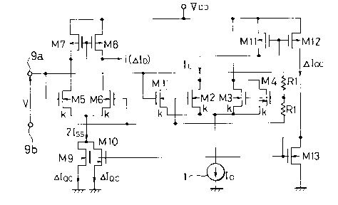
Fig. 5 shows the differential amplifier circuit according
to the first embodiment using a quadritail circuit, which
includes a quadritail circuit and a differential pair of MOS
transistors.
In the quadritail circuit, a first transistor pair is
2102661
composed of N-channel MOS transistors M1 and M2 whose drains are
connected in common, and a second transistor pair is composed
of N-channel MOS transistors M3 and M4 whose drains are
connected in common. The sources of the transistors M1, M2, M3
and M4 are connected in common and between the sources thus
common-connected and the ground, there is provided with a
constant current source 1 (current: Io) for driving the first
and second transistor pairs.
The transconductances parameters of the transistors M1, M2,
M3 and M4 are equal to be k.
The gate of the transistor M1 is connected to one terminal
9a of an input terminal pair and the gate of the transistor M2
is connected to the other terminal 9b of the input terminal
pair. The gates of the transistors M3 and M4 are connected in
common to be connected to the gate of the transistor M1 through
a first resistor. The common-connected gates of the transistors
M3 and M4 are connected to the gate of the transistor M2 through
a second resistor. The resistance of the first and second
resistors are equal to be R1.
An input voltage v is applied between the gates of the
transistors M1 and M2 with the gate of the transistor M2 being
as the st~n~rd. The common-connected gates of the transistors
2102661
M3 and M4 are biased by the middle point voltage (1/2)v of the
input voltage V.
The drains of the transistors M1 and M2 are connected in
common and between the drains thus common-connected and a
voltage source (voltage VDD) a current mirror circuit is
provided. The current mirror circuit is composed of P-channel
MOS transistors M11 and M12 acting as an active load of the
quadritail circuit. The common-connected drains of the
transistors M1 and M2 are connected to the drain and gate of the
transistor M11. The drains of the transistors M3 and M4 are
connected in common to the voltage source.
The differential output current ~IQc of the quadritail
circuit is derived from the drain of the transistor M12 of the
current mirror circuit.
The differential pair is composed of N-channel MOS
transistors M5 and M6 whose transconductance parameters are
equal to be k. The sources of the transistors M5 and M6 are
connected in common to each other, and between the sources thus
common-connected and the ground there are provided with N-
channel MOS transistors M9 and M10, which act as a current
source for driving the differential pair. The gates of the
transistors M5 and M6 are connected to the terminals 9a and 9b,
2102661
respectively, so that the differential input voltage v is
applied between the gates of the transistors M5 and M6.
The drains and gates of the transistors M9 and M10 are
connected to each other, respectively, and the sources thereof
are grounded. The drains of the transistor M9 and M10 are
connected to the common-connected sources of the transistors M5
and M6 and the common-connected sources of the transistors M9
and M10 are connected to the gate of an N-channel MOS transistor
M13. The gate and drain of the transistor M13 are connected to
each other and the source thereof is grounded. The drain of the
transistor M13 iS further connected to the drain of the
transistor M12.
The transistors M13, M9 and M10 form a current mirror
circuit. The transistors M9 and M10 is driven by the drain
current of the transistor M13, that is the differential output
current ~I~ of the quadritail circuit, thereby supplying a
driving current twice in value as much as the current ~I~ to the
differential pair of the transistors M5 and M6.
In the embodiment, ~I~ = IL is established, so that the
differential pair is driven by a current of 2IL (= 2ISS).
There are provided with P-channel MOS transistors M7 and M8
between the voltage source and the differential pair. The
21~2661
transistors M7 and M8 form a current mirror circuit acting as
an active load of the differential pair. The drains of the
transistors M7 and M8 are connected to the drains of the
transistors MS and M6, respectively, the sources thereof are
connected to the voltage source, and the gates thereof are
connected in common to the drain of the transistor M7. A
differential output current of the differential amplifier
circuit i(~ID) is derived from the drain of the transistor M8.
With the differential amplifier circuit of the first
embodiment, the differential pair of the transistors M5 and M6
is driven by the current 2ISs, so that the current ~ID is
expressed as the following equations
i = V {k(4ISS ~ kV2)}1/2 (15)
Here~ ISS = ~IQC = IL is established, so that the following
equation (16) is obtained by using the equation (13-2).
i = V (2kIO)1/2 ¦V¦ S (2IO/3k)1/2 (16)
AS a result, from the equation (16), the transconductance
gm is expressed as the following equation ( 17).
2:102~ l
gm = di/dv = (2kIo)l/2 Ivl S (2Io/3k)1/2 (17)
Fig. 6 shows the input-output characteristic of the
differential amplifier circuit, in which the abscissa indicates
the normalized input voltage, similar to Fig. 4.
From Fig. 6, it is seen that the transconductance gm has a
good linearity in the range of Ivl < (2Io/3k)l/2. This means that
the input voltage range showing the exactly linear
transconductance gm is expanded compared with that of the
conventional differential amplifier circuit shown in Fig. 1.
As described above, with the differential amplifier circuit
of the first embodiment, the differential output current of the
quadritail circuit drives the differential pair of the
transistors M5 and M6, so that linearity of the transconductance
can be ensured in the input voltage range of the quadritail
circuit.
Additionally, the differential amplifier circuit may be
composed of N- and P-channel MOS transistors having the same
transconductances, it can be realized on CMOS integrated
circuits easily.
[Second Embodiment]
2102661
Fig. 7 shows a differential amplifier circuit of a second
embodiment. Similar to the first embodiment, the circuit
includes a quadritail circuit and a differential pair of MOS
transistors. However, it is different from that of the first
embodiment in that the differential pair composed of the
transistors M5 and M6 is driven by a constant current source 2
(current: Io) and an N-channel MOS transistor M14 connected in
parallel and that a current mirror circuit composed of P-channel
MOS transistors M 15 and M16 is provided as an active load of
the quadritail circuit.
The differential output current ~IQC Of the quadritail
circuit is derived from the current mirror circuit of the
transistors M11 and M12 through the current mirror circuit
of the transistors M15 and M16. The current ~IQC drives the
transistor M14 through the transistor M13 to generate a current
equal in value to the current ~IQC. Therefore, the driving
current 2ISs for the differential pair satisfies the equation as
2ISS = IO + ~IQC- This means that the differential pair of the
transistors M5 and M6 is driven by a current equal in value to
the sum of the current Io of the constant current source 1 and
the output current ~IQC Of the quadritail circuit.
With the differential amplifier circuit of the second
23
21026~
embodiment, the same equation as the equation ( 16j can be
obtained, so that the circuit has the same input-output
characteristics as shown in Fig. 6.
[Third Embodiment]
Fig. 8 shows a differential amplifier circuit of a third
embodiment. The circuit is similar in configuration to the
first embodiment with respect to the transistors M1 to M4, the
first and second resistors and the first constant current source
1, which forms the quadritail circuit, and the current mirror
circuit composed of the transistors M7 and M8, which acts an
active load of the differential pair of the transistors M5 and
M6. However, it has the following differences:
First, there is provided with a current mirror circuit
composed of P-channel MOS transistors M15 and M16 between the
quadritail circuit and the voltage source acting as an active
load of the quadritail circuit, instead of the transistors Mll
and M12.
Second, between the common-connected drains of the
transistors Ml and M2 and the common-connected sources of the
transistors M5 and M6, there is provided with an N-channel MOS
transistor M14 whose drain and gate are connected to each other.
24
21026~1
The transistor M14 iS, similar to the transistor M25 of the
conventional differential amplifier circuit shown in Fig. 1, a
current level shifter for shifting a current level between the
common-connected drains (or at a point A) of the transistors M
1 and M2 and the common-connected sources (or at a point B) of
the transistors M5 and M6.
Third, there is a constant current source 3 generating a
current bIo, where b is a constant, between the point A and the
voltage source. In addition, between the point B and the
ground, there is a constant current source 4 generating a
current cIo, where c is a constant, instead of the transistors
M9 and M10 shown in Fig. 5. The differential pair composed of
the transistors M5 and M6 iS driven by the constant current
source 4.
The transistor M14 iS supplied with a current equal in value
to the sum (bIo ~ ~IQC) Of the differential output current -~IQC
of the quadritail circuit and the constant current bIo. Then,
the following equations (183 and (19~ are obtained due to
Kirchhoff's law.
ID1 + ID2 + bIO ~ ~IQC = CIo (18)
IDS + IDS = (C - b)IO + ~IQC (19)
210266 1
Accordingly, the differential output current i(~ID) of the
differential amplifier circuit, which is derived through the
active load of the transistors M7 and M8, is expressed as the
following equation (20) similar to the equation (15).
i = V tk {4(ID5 + ID~) - kv2}]1/2 (20)
With the differential amplifier circuit of the third
embodiment, the same equation as the equation (16) can be
obtained, so that the circuit has the same input-output
characteristics as shown in Fig. 6.
The constants b and c are required to satisfy the
relationships of b 2 1 and c - b 2 0. Preferably, the constants
b and c are set as b = 1 and c = 2 since the input voltage range
in which the transconductance is linear becomes the widest.
There is an advantage that the input voltage range in which
the linearity of the transconductance is good can be changed by
adjusting the current values of the current sources.
The circuit of the third embodiment is similar in
configuration to the conventional one shown in Fig. 1, however,
it has an improved linearity of the transconductance and can be
realized on CMOS integrated circuits easily.
26
21 ~2~61
[Fourth Embodiment]
Fig. 9 shows a differential amplifier circuit of a fourth
embodiment, in which the active load for the differential pair,
which is composed of the transistors M7 and M8, a differential
pair composed of transistors M5" and M6", the transistors M1,
M2, M3 and M4 forming the quadritail circuit, and the constant
current source (current: Io) are stacked in this order between
the voltage source and the ground.
The quadritail circuit is similar in configuration to the
first embodiment in Fig. 5 except for the following:
The gate of the transistor M1 is connected to the terminal
9a of the input terminal pair through a DC voltage source 11
(voltage: Vc) acting as a voltage level adjuster. Thus, the
common-connected gates of the transistors M3 and M4 are also
connected to the terminal 9a through the DC voltage source 11
and the first resistor.
Similarly, the gate of the transistor M2 iS connected to the
terminal 9b of the input terminal pair through a DC voltage
source (voltage: Vc) 12 acting as a voltage level adjuster. The
common-connected gates of the transistors M3 and M4 are also
connected to the terminal 9a through the DC voltage source 12
and the second resistor.
27
2102661
The voltage sources 11 and 12 are provided so that their
positive ends are connected to the terminals 9a and 9b
respectively, as shown in Fig. 9.
With the differential pair, it is different from the first
embodiment in that the transistors M5" and M6" have the
transconductance parameters (k/2) as well as it is driven by the
output current IL Of the quadritail circuit.
The differential input voltage v is applied between the
gates of the transistors M5" and M6" and the voltage obtained
by changing the voltage level of the input voltage v is applied
to the gates of the transistors M1, M2, M3 and M4. The amount
of voltage change is set in accordance with the difference of
their transconductance parameters.
With the differential amplifier circuit of the fourth
embodiment, the same input-output characteristics as shown in
Fig. 6 can be obtained. In addition, there is an disadvantage
that the voltage VDD Of the voltage source is required to be a
little higher than those of the first to third embodiments,
however, the differential circuit is driven by the output
current Io of the quadritail circuit, so that there is an
additional advantage that current consumption can be reduced
compared with the first to third embodiments.
28
2102661
[Fifth Embodiment]
Fig. 10 shows a differential amplifier circuit of a fifth
embodiment, which is similar in configuration to the fourth
embodiment excepting that the DC voltage sources 11 and 12
acting as voltage level adjusters are provided on the sides of
the transistors M5" and M6".
The differential input voltage v is applied between the
gates of the transistors M1 and M2 and the voltage obtained by
changing the voltage level of the input voltage v is applied to
the gates of the transistors M5" and M6".
The voltage sources 11 and 12 are provided so that their
negative ends are connected to the term1nals 9a and 9b
respectively, as shown in Fig. 10.
As described above, the MOS quadritail circuit has the wider
input voltage range generating the exact square-law
characteristic than the prior art although it is simple in
configuration. Therefore, with the differential amplifier
circuits of the first to fifth embodiments, there are an
advantages that linearity of their transconductances can be
improved.
29
2102~1
In addition, since the transistor pair is composed of MOS
transistors having the same transconductance parameter, the
problems of the prior art do not occur and therefore, the
differential amplifier circuits of these embodiments can be
realized on CMOS integrated circuits easily.
Further in addition, in the quadritail circuit, the
transistors M3 and M4 have sources, drains and gates connected
in common, respectively. Therefore, one MOS transistor which
is twice in capacity or transconductance parameter as much as
the transistor M3 or M4 may be used in place of the pair of the
transistors M3 and M4.