Note: Descriptions are shown in the official language in which they were submitted.
2la4~
PAT~NT
2228-33-00
CHENICAL VAPOR DEPO~ITION-PRODUCED SILICON CARBIDE
HAVINa IMpRov~n PROP~T~S
The pre6Qn~ invQntion ~ dlroct~d to eilicon carbiae produced
by chemical vapor deposi~ion proce~se6 havin~ improve~ opt~cal
properties, including improved optica~ transmission, purity, and
electrical resistivity, and to a d~position pro~es~ for produc~ng
suqh silicon carbid~.
~o ~çkoround o~ ~he ~nventton
While single cry tal ~-SiC exhibits some degree o~ optical
transmiss~on, polycry~talline ~ is sub6~antially opaque. It
would be dQsirabl~ to prov~de B-SiC which opt~cally transmits,
p~rt~cularly ~n the vi~i~le and in~rared range. Opt~cal~y
tranemitting SiC would hav~ applications for lonses and domss,
l~ght d~tection and ranging ~T.I~AR) mirrorg, solar collectore and
concentrator8, cathod~ cov~rs (in the reactive ion etching
sy~tems), and astronomical mirror6. Slngle crystal a-SlC ~
unsuitab~e for such bulk applications duo ~o it~ ~izo limitation;
t~u~, it would bQ d~sirable to produce optically tran~mittin~ B-S$C
which can be produced ln bulk.
Known bulk ~ilicon car~ide is almost invariably opaque,
absorbing and scattering li~ht in the visi~lQ and infrar~d ~egions
of the ~p~ctrum. Method~ o~ producing bUlk SiC includ~ sint~ring
and hot p~e~ing, slip castinc~ and reac~ion bonding~ The~ m~thods
are unlikely c~nd~dat~s for produc~ng opt~cally transmitting SlC ag
th~y suff~r from one or more of the following drawbac~ hey
produco a multi-pha~e mater1al, e.g., in~lude a Si p~e, 2) the
~ater~al iQ not theoretically dense, andlor 3) the material is not
cf high purity and may contaln metall~c impuriti~6 that d~grad~
optical transmiB~ ion.
A better candidate ~or producing op~lcally transm~tting SiC,
e~the~ free-standing bulk SiC or thin films on a subs~rat~ sur~ac~,
CA 02104411 1998-10-02
PATENT
2228-33-00
is SiC produced by chemical vapor deposition (CVD). However,
most of the SiC previously produced by CVD is opaque,
exhibiting considerable scattering and absorption in the
visible and infrared. Applicants are aware of efforts by the
U.S. Air Force and General Electric to improve the infrared
transmission of SiC by improving process parameters, such as
substrate temperature, flow rates, furnace pressure etc.
These efforts met with limited success. Although SiC
transmitted in the 2-5~m (infrared spectrum range), the
material exhibited considerable scattering which made it
unsuitable for use in imaging applications.
It is a general object of the present invention to
produce B-SiC in bulk or thin film form having improved
optical transmission. Other objects include providing CVD-SiC
having heretofore unachieved purity, and electrical
resistivity.
Summary of the Invention
Bulk, free-standing, silicon carbide, fabricated by
chemical vapor deposition (CVD), is optically transmitting in
the visible and infrared range. Specific deposition
parameters are required to produce the optically transmitting
silicon carbide. This silicon carbide is highly pure,
theoretically dense and has electrical resistivity in excess
of SiC's previously known.
Brief Description of the Drawings
Fig. l is a schematic of CVD apparatus used to fabricate
optically transmitting B-SiC.
Fig. 2 is a graph comparing the transmission of CVD-B-SiC
with the transmission of ~-SiC.
Figs 3a, 3b and 3c illustrate different baffle/mandrel
arrangements used within the deposition chamber of a furnace
for the fabrication of CVD-~-SiC.
21Q 14~1
PATENT
2228-33-00
Fig. 4 is a transmission spectrum of a highly optically
transmitting CVD-B-SiC.
Detailed DescriPtion of Certain Preferred Embodiments
S Herein, unless otherwise noted, optical properties of silicon
carbide produced in accordance with the present invention are
defined in terms of Attenuation Coefficients (cml) at 0.6328 ~m
(visible-laser measured) and 3 ~m (infrared-spectrophotometer
measured). Attenuation coefficient is intended herein to include
all optical losses, including both scattering and absorption.
Attenuation coefficient is calculated as follows. If T, R, x are
the transmittance, reflectance and material thickness, then the
attenuation coefficient, B is calculated from the following
equation
(1-R~2 exp(-Bx)
T
1-R exp(-2~x)
The reflectance is calculated from the refractive index (n).
(n-1)
R = 2
(n+1)
The refractive index (n) is assumed to be 2.635 at 0.6328 ~m and
2.555 at 3 ~m.
Unless otherwise stated, properties of SiC produced in
accordance with the invention are room temperature values, i.e.,
measured at 20-28~C (293-301~K). Although it is believed that
thermal conductivity measurements are generally independent of the
measuring technique, thermal conductivity values reported herein
are those measured by flash-lamp techniques. Deposition chamber
temperatures are measured by thermal probes within the deposition
chamber placed closely adjacent the deposition site, e.g., a
mandrel on which bulk free-standing SiC is to be deposited or a
surface on which a film of SiC is to be deposited. Although the
deposition site temperature may not be exactly that of the probe-
~ 1~4~ ~
PATENT
2228-33-00
measured location, experience has found that probes closely
adjacent, but differently located relative to a deposition site are
almost always within 10~C of each other and generally within 5~C of
each other. Thus, the deposition site is presumed to be within 5-
10~C of the probed deposition chamber temperature.
The SiC to which the invention pertains is bulk or free-
standing, i.e., capable of being self-supported. This is to be
distinguished from thin SiC films which are deposited upon a
surface with the intent that the SiC remain permanently bonded
thereto. To be free-standing, the SiC must generally be deposited
to a thickness of upward of about 0.1 mm.
Silicon carbide produced in accordance with the present
invention has an attenuation coefficient at .6328 ~m of about 20
cm1 or less, preferably about 10 or less, and more preferably
about 8 or less. The silicon carbide has an attenuation
coefficient at 3 ~m of about 20 cm1 or less, preferably about 10
or less, more preferably about 8 or less and most preferably about
5 or less. It is believed that silicon carbide produced in
accordance with the present invention is more optically
transmitting at .6328 and 3 ~m than any polycrystalline silicon
carbide of the prior art. The silicon carbide in accordance with
the invention is stoichiometric (1:1 Si:C ratio), 100% theoretical
dense, and highly pure, i.e., about 5 ppm metallic impurities or
less and preferably about 3.5 ppm metallic impurities or less. It
is found that the higher is the purity, the greater is the optical
transmittance of the SiC produced. Also high purity is very
important for semiconductor furniture manufactured of CVD-SiC.
High purity is achieved using high purity reaction materials,
particularly 02-free H2 and contamination free graphite
deposition set up. It has been demonstrated that distilling
methyltrichlorosilane (MTS) from its as-purchased condition
results in more optically transmitting CVD-deposited SiC.
Another feature of the SiC of the present invention is its
F~
i
PATENT
2228-33-00
very high bulk resistivity. Resistivity is an important attribute
of material for electronic pac~aging. The upper limit of most non-
doped SiC to date is about 100 ohm-cm, and CVD-SiC is not believed
to have been consistently produced having resistivity of more than
100 ohm-cm. The resistivity of CVD-SiC according to the present
invention has reached 4.53xlO ohm-cm. When SiC of such high
electrical resistance is achievable, values lower than this value,
yet still above that known in the prior art, is achievable, by
introduction of impurities, e.g., through doping. Accordingly,
novel CVD SiC is produced in accordance with the present invention
having resistivity of 500 ohm-cm or greater, preferably 1000 ohm-cm
or greater, and more preferably 10,000 ohm-cm or greater.
Furthermore, the SiC produced in accordance with the invention is
of the n-type, whereas most CVD-SiC is of the p-type. n-type is
preferred as its resistivity tends to be constant over a broader
temperature range.
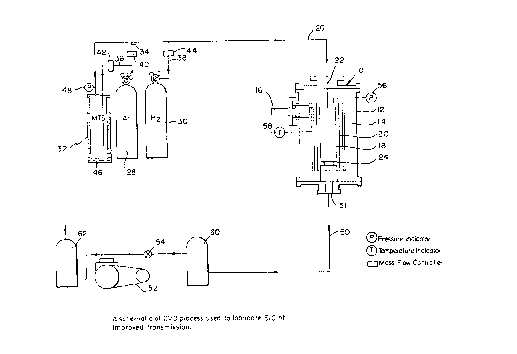
Illustrated in Fig. 1 is an apparatus useful for fabricating
CVD-~-SiC. Deposition is carried out within a furnace 10. A
stainless steel wall provides a cylindrical deposition chamber 12.
Heating is provided by a graphite heating element 14 which is
connected to an external power supply by an electrode 16. Graphite
deposition mandrels 18 are arranged within a graphite isolation tube
20 and gas is introduced by means of an injector 22 through the
upper end of the isolation tube so that the reaction gases sweep
along the mandrels 18. One or more baffle(s) 24 is used to control
the aerodynamics of gas flow through the furnace.
The line 26 which supplies the injector is fed by an argon
cylinder 28, a hydrogen cylinder 30, and a methyltrichloro-silane
(MTS) bubbler 32. The argon is fed by lines 34 and 36 both
directly to inlet line 26 and through the bubbler 32. The
hydrogen cylinder is connected by a line 38 to the inlet line 26.
Argon flow through lines 32 and 36 and hydrogen flow through line
38 are controlled by mass flow controllers 40, 42 and 44. The
methyltrichlorosilane (MTS) cylinder 32 is maintained at a
s
A ~
PATENT
2228-33-00
constant temperature by a constant temperature bath 46. A pressure
gauge 48 is connected to a feed back loop which controls the gas
pressure of the bubbler 32.
An outlet line 50 is connected to a bottom outlet port 51.
Pressure within the deposition chamber 12 is controlled by a vacuum
pump 52 which pulls gases through the chamber and a furnace
pressure control valve 54 operably connected to the vacuum pump.
The temperature and pressure within the deposition chamber 12 are
measured by a thermal probe 58 and a pressure indicator 56.
Exhaust gases are passed through a filter 60 to remove particulate
material upstream of the pressure control valve and through a
scrubber 62 downstream of the vacuum pump to remove HCl.
As discussed below in the examples, particularly with respect
to Figs. 3a, 3b and 3c, the arrangement of baffles may be varied to
produce desired results. The results discussed below with respect
to Figs 3a, 3b and 3c are particular to the furnace in which the
SiC was deposited and may vary from furnace to furnace and also the
configuration of the mandrel or substrate on which SiC of desired
configuration is to be deposited.
To obtain optically transmitting CVD-deposited ~-SiC, a
deposition chamber temperature of between about 1400 and about
1500~C, preferably between about 1400 and about 1450~C is employed.
The deposition chamber pressure is about 50 torr or lower,
preferably about 10 torr or lower and most preferably about 5 torr
or lower. The H2/MTS ratio is from about 4 to about 30, preferably
from about 10 to about 20. The deposition rate is about 1 micron
per minute or less; it is believed that this very low deposition
rate is critical to obtain ~-SiC with good optical transmittance.
The rate at which the deposition surface is swept by the reactant
gases also appearS to affect the optical transmittance of the
deposited SiC. Although optically transmitting SiC has been
produced with average flow velocities of about 10 cm/sec, it is
preferred that flow velocities be at least about 300 cm/sec, and
, ~ ~.
A~
PATENT
2228-33-oO
more preferably at least about 1000 cm/sec. Sweep velocity, which
is the gas velocity at the deposition surface, is a function not
only of the ~low rate of gases into the furnace, but of the furnace
design and orientation of the deposition surface(s) within the
deposition chamber of the furnace.
HCl is a reaction product of the deposition of SiC using MTS
and H2 as the reaction gases. It is found that adding gaseous HCl
to the gas stream that is introduced into the reaction chamber
further improves the optical transmission of the CVD-B-SiC which is
produced. To have a significant effect on transmission of the SiC,
the HCl/MTS molar ratio is generally at least about 0.2.
The invention will now be described in greater detail by way
of specific examples in the experiments described below.
ExamPle 1
Several depositions of SiC were performed in a CVD reactor to
fabricate CVD-SiC with improved transmission. In these
depositions, the CVD process conditions and the deposition set-up
were varied to optimize the vis-IR transmission of CVD-SiC. The
process conditions used were: substrate temperature: 1400-1470~C,
furnace pressure: 3-200 torr, flow rates - MTS: 0.1-2.8 slpm
(standard liters per minute), H2: 0.5-5.8 slpm. H2/MTS molar
ratio: 4-30, and average flow velocity = 14-1260 cm/sec.
The CVD-SiC was characterized for vis-IR transmission. The
SiC transmission was determined to be dependent upon methyltri-
chlorosilane (MTS) purity, CVD process conditions and CVD
deposition geometry. The commercially available MTS of 99% purity
contains metallic impurities which end up in the CVD-SiC and
degrade its near-IR transmission. Distillation of methyltri-
chlorosilane (MTS) in a narrow temperature range around its
boiling point has resulted in fabricating SiC which exhibits good
transmission in the infrared region.
Table 1 below ~hows the attenuation coefficient values for
CVD- SiC at 0.6328 ~m and 3 ~m as a function of furnace pres~ure.
,.
A ~
21~4~ i
PATENT
2228-33-00
It is seen that as the pressure decreases from 200 torr to 10 torr,
both visible and infrared attenuation coefficients decrease, i.e.,
transmittanGe in both visible and infrared regions increase.
Although Run #11 (furnace pressure = 3 torr), material showed an
increase in attenuation coefficient in comparison to Run #7
(furnace pressure = 10 torr), this increase may be due to the
deposition set-up which was changed.
The effects of varying other CVD process parameters on
transmission were less clear. Optimum results were obtained for
the following process conditions. Substrate temperature: 1425~C,
Furnace pressure: 10 torr, Flow rate: MTS = 0.19 slpm, H2 = 2.8
slpm, Ar = 1.0 slpm, H2/MTS molar ratio = 15 and average flow
velocity = 365 cm/sec.
Three deposition set-ups were tried in an effort to maximize
the transmission of CVD-SiC. These set-ups are shown in Figure 3a,
3b and 3c. All these set-ups yielded CVD-~-SiC with improved
transmission at different parts of the deposition region. Two set-
ups (Figs. 3a,b) used four rectangular mandrel plates, 3.5 in.-wide
x 12 in.-long, arranged in the form of an open square box.
The deposition set-up of Figure 3a consisted of a mandrel box
100 at the end of which was placed a graphite baffle 102. In this
case, porous material was deposited on the mandrel while dense and
good quality ~-SiC was obtained on the baffle. It is believed that
the porous material was deposited because (i) the reagents were
"cold," i.e., there was considerable temperature difference between
the mandrel and the gaseous reagents and (ii) the reagent sweep
speed on the mandrel walls was small. This explanation is
consistent with the observation that the material on the upper half
of the mandrel was more porous than on the lower half.
In Figure 3b two baffles were used, one 104 before and the
other 106 after the mandrel box. The function of the first baffle
104 is to preheat the reagents and direct the gas close to the
mandrel walls to increase reagents sweep speed along the mandrel
21~411
PATENT
2228-33-00
box 108. This deposition set-up produced CVD ~-SiC with good vis-
IR transmission. The "best" material was produced on the upper
half of the the mandrel box. The deposited material on other areas
had better transmission than that produced at other CVD conditions.
In the deposition set-up of Figure 3c, the two walls of the
mandrel box 110 were tapered. The cross-section of the mandrel box
was a square 3.5 in. x 3.5 in. on the top end and a rectangle 3.5
in. x 1.05 in. at the bottom end. The aim of using this tapered
box was to continuously reduce the cross-section and thus increase
the flow velocity to study its effect on the quality of the
material. This set-up also employed a baffle 112 before and a
baffle 114 after the mandrel box. Although this configuration also
produced good optical quality CVD-SiC, considerable stress in the
material was observed and the deposited material exhibited
substantial bowing.
Table 1
Attenuation Coefficient of CVD-~SiC as
Function of Furnace Pressure
Attenuation Avg
Run Furnace Furnace Pressure Coefficient (cm') Veloci
No. Set-Up(Torr) ~ 0.6328 ~ma 3~.1n ty
cm/sec
2 3a 200 30 40 49
3 3b 200 66 24 21
4 3b 40 19 21 197
3c Z0 16 14 272-
761
7 3b 10 7.3 3.5 365
3 0 11 3b 3 - 7.6 1260
PATENT
2228-33-00
ExamPle 2
Addition of HCl to the reaction mixture is found to suppress
formation of Si-rich SiC. The CVD process conditions were:
substrate temperature = 1413-1423~C, Furnace pressure: 3-7 torr,
flow rates - H2: 2.8 slpm, MTS: 0.19 slpm, Ar: 1.0 slpm, HCl:
0.15-6.0 slpm, H2/MTS molar ratio: 15, HCl/H2 molar ratio = 0.054
- 0.21 and an average flow velocity: 540-1260 cms . The
deposition set-up used was the two-baffle configuration of Figure
3b. Table 2 below lists the attenuation coefficient values that
were obtained when HCl was added to the reagent mixture. A
comparison of attenuation coefficient for Run #10 and #11 (Table 1)
clearly shows improved optical transmission values when HCl is
added. Further, similar to Example 1, the vis-IR transmittance of
CVD-SiC increased as the furnace pressure decreased.
Table 2
Attenuation Coefficient of CVD-~SiC when HCl
is Added to the Reaction Mixture
Average
Run Furnace Furnace Attenuation Velocity
No. Setup Pressure Coefficient (cm) cm/sec
(Torr)
Q 0.6328 ~m @ 3~m
9 3b 7 7.4 2.8 540
10 3b 3 6.9 2.1 1260
Figure 2 shows a comparison of transmission of ~-SiC with that of a
commercially available ~-SiC single crystal sample. Both samples
are 0.012-inch thick. It is seen that CVD-~ SiC performs
considerably better than single crystal ~-SiC in the near-IR region
while the latter material performs better in the visible region.
A
PATENT
2228-33-00
Figure 4 shows infrared transmission of CVD-SiC when HCl is
added to the reaction mixture (Run #lO). The thickness of the
sample was about 0.022-inch. 60% transmission is seen in the near
IR region which corresponds to an attenuation coefficient of
2.1 cml at 3 ~m. This is believed to be the lowest value of
specular attenuation coefficient that has ever been achieved for a
polycrystalline CVD-~SiC free-standing sample. This material was
also characterized for hardness and fracture toughness and yielded
values of Vickers hardness (Kg mm 2~ = 2700 +58.8 with 1 Kg load
and fracture toughness (MN m /) = 2.23 +0.043. These values are
typical of CVD-SiC. Thus, an improvement in optical properties has
been obtained without degrading other properties such as hardness
and fracture toughness.
While the invention has been described in terms of certain
preferred embodiments, modifications obvious to one with ordinary
skill in the art may be made without departing from the scope of
the invention.
Various features of the invention are set forth in the
following claims.