Note: Descriptions are shown in the official language in which they were submitted.
` 210~3~
INVERTER DEVICE
BACKGROUND OF THE INVENTION
This invention relates to an inverter device in
which part of a high frequency output of an inverter
circuit is caused to feedback to a rectifier, and a
high-frequency current supply to the rectifier is made
possible substantially over the entire range of an AC
source voltage, so as to improve the input power-factor.
DESCRIPTION OF RELATED ART
For known inverter devices suggested for
improving the input power-factor and the efficiency, there
has been shown in, for example, Japanese Patent Laid-Open
Publication No. 4-193067 by M. Maehara an inverter device
which has been used as a discharge lamp lighting device.
More specifically, this discharge lamp lighting device
comprises a diode bridge acting as a rectifier for an AC
source voltage, a smoothing capacitor for smoothing an
output of the diode bridge, an inverter circuit including
a vibration system and converting a voltage across the
smoothing capacitor into a high frequency voltage as an
output, and an input power-factor improving circuit which
causes part of the high frequency output of the inverter
circuit to feedback through at least a further capacitor
as an impedance element to a DC output end of the diode
bridge and carries out a high-frequency current supply to
the diode bridge substantially over the entire range of
the AC source voltage.
In the inverter circuit of this inverter device,
2104737
.,
a pair of switching elements are connected in series to
both ends of the smoothing capacitor, a discharge lamp is
connected across one of the pair of switching elements
with a DC-component cutting capacitor and an inductor
interposed, and a preheating capacitor for filaments of
the discharge lamp is connected across non-source side
ends of the filaments. In this case, the preheating
capacitor constitutes along with the inductor the
oscillatory system contained in the inverter circuit.
In the above inverter circuit, the voltage
across the smoothing capacitor is converted into the high
frequency voltage by means of alternate high-frequency
turning ON and OFF of the pair of switching elements, for
the purpose of a high-frequency lighting of the discharge
lamp. That is, the discharge lamp is subjected to such
high-frequency lighting that, when first one of the pair
of switching elements is turned ON, the high frequency
voltage is supplied to the discharge lamp through the
smoothing capacitor, the first switching element, the
inductor and the DC-component cutting capacitor, and, when
second one of the switching elements is turned ON with a
charge accumulated as a power source in the DC-component
cutting capacitor during the above voltage supply, the
power is supplied to the discharge lamp in reverse
direction to that upon the turning ON of the first
switching element through the DC-component cutting
capacitor, the inductor and the second switching element.
In the input power-factor improving circuit of
210~737
the foregoing discharge lamp lighting device, the circuit
comprises the capacitor as the impedance element connected
between a juncture of the DC-component cutting capacitor
to the discharge lamp and a positive pole side output end
of the diode bridge, and a diode connected between the
positive pole side output end of the diode bridge and the
smoothing capacitor. In the discharge lamp device
including this input power-factor improving circuit, at
the time of the turning ON of the second one of the pair
of the switching elements, a current is caused to flow
through a path of the diode bridge, capacitor as the
impedance element, DC-component cutting capacitor,
inductor and second switching element, and further an
inverted current is caused to flow, due to an action of
the oscillatory system comprising the capacitor as the
impedance element and inductor during ON state of the
first one of the pair of the switching elements, mainly
through a path of the capacitor as the impedance element,
power-factor improving diode, first one of the pair of
switching elements, inductor and DC-component cutting
capacitor.
Thus the input power-factor can be improved by
means of the high-frequency supply of current through the
impedance-use capacitor to the diode bridge over the
entire range of the AC source voltage, and, accordingly,
the input power-factor improvement can be executed by such
simple measure of adding the impedance-use capacitor and
diode.
210g737
In the foregoing known inverter device employed
as the discharge lamp lighting device, however, there
arises such problem that a ripple component is caused to
become remarkable upon oscillation in the switching
frequency of the pair of switching elements, giving an ill
influence on the operation of such load as the discharge
lamp, in which event a flicker or the like is likely to
occur in light output of the discharge lamp.
SUMMARY OF THE INVENTION
Accordingly, an object of the present invention
is to provide an inverter device which is capable of
overcoming the foregoing problem in the known art and, in
particular, remarkably reducing the ripple component which
exerts ill influence upon the load of the device the input
power-factor of which is attempted to be improved by
causing part of high frequency output to feedback to the
rectifier for an AC source voltage and attaining the
high-frequency current supply to the rectifier
substantially over the entire range of the AC source
voltage.
According to the present invention, the above
object can be realized by an inverter device in which an
AC source voltage is rectified by a rectifier, a rectified
output of which is smoothed through a smoothing capacitor,
a voltage across the smoothing capacitor is converted into
a high frequency voltage by an inverter circuit including
a first oscillatory system, an input power-factor
improving circuit causes part of a high frequency output
2104737
"". . ,
of the inverter circuit to feedback through an impedance
element to a rectified output end of the rectifier and a
high-frequency current supply to the rectifier to be
effected substantially over the entire range of the AC
source voltage, and the impedance element in the inverter
circuit and connected to the rectified output end of the
rectifier constitutes at least part of the first
oscillatory system as well as a second oscillatory system,
wherein the inverter circuit is operated by a control
means in the first and second oscillatory systems with a
fixed frequency which renders supplied output to a load
substantially constantly equal.
Other objects and advantages of the present
invention shall be made apparent in following description
of the invention detailed with reference to preferred
embodiments shown in accompanying drawings.
BRIEF DESCRIPTION OF THE DRAWINGS
FIGURE 1 shows in a circuit diagram an
embodiment of the inverter device according to the present
invention;
FIG. 2 shows in waveform diagrams the operation
of the circuit in FIG. l;
FIGS. 3 and 4 are explanatory circuit diagrams
for mutually different operational modes of the embodiment
in FIG. l;
FIG. 5 is a characteristic diagram in respect of
two oscillatory systems occurring in the circuit of FIG. 1
upon the different operational modes;
~ 2104737
FIGS. 6 and 7 are circuit diagrams for
explaining the two oscillatory systems occurring in the
circuit of FIG. l;
FIG. 8 is an output diagram of an inverter
circuit included in the device of FIG. 1 with respect to a
source voltage;
FIG. 9 is an explanatory waveform diagram for
obtaining the output diagram of FIG. 8;
FIG. 10 shows in a circuit diagram another
embodiment of the inverter device according to the present
invention;
FIGS. 11 and 12 are different output
characteristic diagram with respect to a rectified output
in the circuit of FIG. 10; and
FIGS. 13 through 36 are circuit diagrams showing
other embodiments of the inverter device according to the
present invention.
It should be appreciated here that, while the
invention should be described with reference to the
embodiments shown in the accompanying drawings, the
intention is not to limit the invention only to these
embodiments but is to rather include all alterations,
modification and equivalent arrangements possible within
the scope of appended claims.
DETAILED DESCRIPTION OF THE PREFERRED EMBODIMENTS
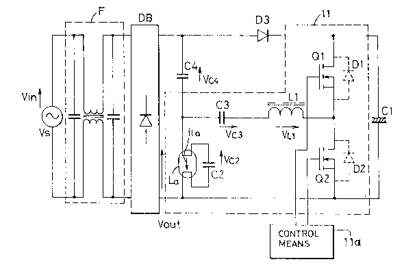
Referring here to FIG. 1, there is shown in a
circuit diagram an embodiment of the inverter device
according to the present invention, and references shall
2104737
be first made to an occurrence of ripple component to be
reduced according to the present invention, for promotion
of better understanding of the present invention. The
device comprises an inverter circuit 11, and a capacitor
C4 connected thereto as an impedance element is to be
charged in a direction denoted by an arrow in FIG. 1 when
a current flows from a diode bridge DB through a path of
the capacitor C4, DC component cutting capacitor C3,
inductor Ll and second one Q2 of a pair of switching
elements Ql and Q2, in similar manner to the foregoing
known device. On the other hand, the capacitor C4 carries
out a discharge in a path of a current flow mainly through
the capacitor C4, diode D3, first one Ql of the pair of
switching elements, inductor Ll and capacitor C3, upon
which a voltage across the capacitor C4 is caused to be
lowered.
The charge and discharge of the capacitor C4 do
not proceed at the same timing as the turning ON and OFF
of the pair of switching elements Ql and Q2 but are
determined in the relationship of the voltage value with
respect to a voltage Vc4 across the capacitor C4, source
voltage Vin, voltage VLl across the inductor Ll and
voltage Vc3 across the capacitor C3. That is, with the
operating state changed over between those shown in FIGS.
3 and 4, the device output with respect to such source
voltage Vin as shown by a waveform (a) of FIG. 2 is caused
to vary in envelope waveform of the output as shown by
dotted lines of waveforms (b) to (d) of FIG. 2. In such
2104737
state as shown by the waveforms (b) and (d) of FIG. 2, in
particular, a difference between the maximum and minimum
values of the envelope waveforms or, in other words, the
ripple component becomes remarkable. Considering now of a
case in which the second switching element Q2 is ON, there
are present two operational modes, one of which is of a
first oscillatory system, as shown by a dotted line in
FIG. 3, of a current flowing through a path of the
capacitor C3, resonance inductor Ll, second switching
element Q2, resonance capacitor C2 and such load La as a
discharge lamp, and the other of which is of a second
oscillatory system, as shown by a dotted line in FIG. 4,
to which a path from the diode bridge DB, capacitor C4,
capacitor C3, inductor Ll and second switching element Q2
is added, and the circuit operation is changed over
between these two modes within each turning cycle of the
pair of switching elements while change-over timing is
also varied by virtue of the magnitude of the source
voltage Vin in AC cycle. The second oscillatory system
shown in FIG. 4 is connected through the diode bridge DB
to a source so that, with the source voltage Vin made
larger, the term of each cycle of the second switching
element Q2 being changed over to this second oscillatory
system is prolonged, and the entire circuit arrangement is
caused to be affected strongly by the second oscillatory
system.
When on the other hand the load current ila
characteristics are obtained in respect of the first and
21047~7
second vibration systems independently, they will be as
shown in FIG. 5. The load current characteristics of said
first and second vibration systems are respectively shown
by lines of 1 and 2 in FIG. 5. Here, the first
oscillatory system is shown independently as in FIG. 6
while the second oscillatory system is as in FIG. 7. It
is judged that, as seen in FIG. 5, the frequency f in
which the ripple component of the load current ila is the
minimum as the waveform (c) of FIG. 2 is at a state where
the characteristics of both oscillatory systems are
substantially equal. This means that, at a state of f =
f2 where ila in the first oscillatory system ~ ila in the
second oscillatory system, the load current ila is greatly
influenced by the second oscillatory system as the source
voltage Vin is made larger, and the waveform of the load
current ila becomes smaller as shown by (d) in FIG. 2 when
the source voltage Vin is large. When f = fl where ila in
the first oscillatory system < ila in the second
oscillatory system, contrarily, the load current ila will
increase as the waveform (b) in FIG. 2, as the source
voltage Vin increases. Accordingly, the state where the
ripple component of the load current ila becomes the
minimum may be regarded to be that f = fO where ila in the
first oscillatory system is substantially equal to ila in
the second oscillatory system.
Since in this case one that directly
contributive to the occurrence of the ripple component is
the source voltage Vi , output characteristics of the
-- 10 --
- 21047~7
source voltage Vin (in practice, the absolute value IVi I
of tne source voltage Vin because the source voltage is
supplied through the diode bridge to circuits of following
stages) and the inverter device have been obtained, which
are as shown in FIG. 8, wherein the output (for example,
the voltage across the load) is taken on the ordinate
while the absolute value of the source voltage is taken on
the abscissa. In the drawing, the respective absolute
values are all momentary values, and the maximum value Vp
of the source voltage is also shown. More specifically,
when in the inverter device of FIG. 1 the absolute value
¦Vin¦ of the source voltage and an output voltage VOUt are
in such state as shown in FIG. 9, the output VOUt at ¦Vin¦
= 0 is obtainable from a value during a finely short time
~t before and after t = tl, the output VOUt at IVinl = Vp
is obtainable also during the finely short time ~t before
and after t = t3, and similarly the output VOUt at an
optional ¦Vin¦ is obtainable from a value also during the
finely short time ~t before and after a time when ¦Vin¦ is
reached (for example, t = t2). Here, the finely short
time ~t should optimumly be set several times as large as
the frequency of the switching elements used in the
inverter circuit, to render any variation in IVinl to be
of an ignorable level.
As will be apparent from FIG. 8, the output is
made substantially constant when oscillation frequency of
the inverter circuit 11 is made f = fO, and the ripple
component can be reduced. In the embodiment of FIG.
2104737
. , ,
according to the present invention, there is provided a
control means lla so that the inverter circuit 11 will be
operated at the frequency fO at which the outputs of the
two oscillatory systems will be substantially equal to
each other, whereby such change-over operation of the
circuit as shown in FIGS. 6 and 7 can be carried out so as
to minimize output fluctuation, and the ripple component
can be reduced. When the inverter device according to the
present invention is employed in, for example, the
discharge lamp lighting device, therefore, it is made
possible to restrain such problem as flickering, in
particular, from occurring in the discharge lamp as the
load La. It is of course possible to maintain the
improvement in the input power-factor in similar manner as
in the known art having applicable circuit thereto.
In an event when the foregoing inverter circuit
11 is operated at other oscillation frequency than f = fO,
the present invention is to adopt an arrangement for
reducing the ripple component which becomes large as in
(b) or (d) of FIG. 2 without any measure therefor.
Referring to FIG. 10, the control means according to the
present invention comprises a supplied voltage detector 12
for detecting the source voltage Vin, a frequencY
controller 13 for controlling the oscillation frequency f
of the inverter circuit 11 in accordance with a detection
output of the detector 12, and a driving means 14 for
receiving an output of the frequency controller 13 and
controllably driving the pair of switching elements Ql and
- 2104737
Q2. According to this arrangement of FIG. lO, therefore,
the oscillation frequency f of the inverter circuit ll can
be varied in accordance with the variation in the source
voltage Vin which is concerned deeply in the occurrence of
the ripple component, and it is made possible to
effectively reduce the ripple component.
In the present embodiment, the load La is
connected to the resonance capacitor C2 through the
transformer T and is insulated from the source side, but
the circuit operation does not differ from that of the
aspect in which the load is directly connected in parallel
with the capacitor C2. This applies also to a case where
the capacitor C2 and load La are connected on non-source
side of the transformer T, that is, on the secondary side.
More specifically, the relationship between the
source voltage Vin and the output of the inverter circuit
11 in respect of other frequencies f than the frequency fO
at which the ripple component can be reduced, has been
obtained, resultant curves of which are as shown in FIG.
11. As will be evident from the drawing, there are shown
such characteristics that the output VOUt is also made
larger as the source voltage Vin increases when the
oscillation frequency f of the inverter circuit ll is made
to be f<fO, and that the increase in the output VOUt is
made larger as the oscillation frequency f separates from
fo (i.e., fll~fl2 fl3 14 Assuming here, for
example, that the output VOUt is Vl with the source
voltage Vin made 0 at the frequency fll, the output VOUt
2104737
can be made to be Vl by varying the oscillation frequency
f of the inverter circuit 11 in response to the source
voltage Vi as will be clear from FIG. 11. Assuming
further that the source voltage is Vinl and the
oscillation frequency f of the inverter circuit 11 is fl2~
the output VOUt is made Vl, or, when the source voltage is
Vin2 and the oscillation frequency f of the inverter
circuit 11 is fl3, then the output VOUt is also made Vl.
In this case, in the embodiment of FIG. 10, the
oscillation frequency f of the inverter circuit 11 is
smoothly varied by means of the frequency controller 13 in
accordance with the variation in the source voltage Vin.
That is, as will be readily appreciated, the oscillation
frequency f of the inverter circuit 11 is kept lower in
the period when the source voltage Vin rises but, to the
contrary, as the source voltage Vin falls, the oscillation
frequency f of the inverter circuit 11 is raised.
While in the above the reference has been made
to the controlling of the output VOUt to be constant at
the oscillation frequency f lower than the frequency fO
minimizing the ripple component, it is made possible with
the same arrangement to control the output VOUt to be
constant at the frequency f higher than the frequency fO
which minimizes the ripple component as shown in FIG. 12
21 24: here fo~f21~f22~f23~f24).
While it is preferred that the oscillation
frequency f of the inverter circuit 11 in accordance with
the source voltage Vin is selected to be one obtained from
~ 2104737
the characteristics of FIGS. 11 and 12, it is also
possible to remarkably reduce the ripple component even
with a measure of varying the frequency substantially in
proportion to the source voltage Vin as compared with an
event where the frequency is not controlled. Further,
there is a difference in the output VOUt in the event
where the oscillation frequency f is made fO as is clear
in FIG. 8, from that in an event where the frequency f is
made variable but the output VOUt of the inverter circuit
11 is kept constant to be Vl and V2 as has been described
with reference to FIGS. 11 and 12. Accordingly, it is
possible to obtain the output VOUt of the inverter circuit
11 while sufficiently reducing the ripple component by
employing a control means in which the foregoing
arrangement of FIG. 8 and the further arrangement
described with reference to FIGS. 11 and 12 are combined
as shown in FIG. 13.
In a further embodiment shown in FIG. 14, the
circuit arrangement is different from the foregoing
embodiments in respect that the oscillatory system
including the load La of the inverter circuit 11 is
connected to the side of the first switching element Q1,
connecting point of the capacitor C4 and the diode D3 as
well as the direction of the diode D3 are modified in
accordance with the above connection of the oscillatory
system, and the source voltage Vin is detected at output
end of the diode bridge DB, but the operation of the
inverter circuit 11 and the function of reducing the
21~47~7
ripple component are substantially the same as the
foregoing embodiments.
In another embodiment shown in FIG. 15, there
are differences from the foregoing embodiments in respect
of inserting position of the DC component cutting
capacitor C3 and an additional connection, if occasion
demands, of an inductor L2 in series with the
impedance-use capacitor C4 (the inductor being shown as
parenthesized in the drawing), while the operation of the
inverter circuit 11 as well as the function of reducing
the ripple component are substantially the same as those
in the foregoing embodiments. It is also useful to
additionally provide an inductor or capacitor in the
oscillatory systems of the inverter circuit 11 in the
device of the instant embodiment.
On the other hand, an event where the load La is
the discharge lamp which is lighted for being dimmed shall
be considered. In a discharge lamp lighting device of an
inverter type having no input power-factor improving
circuit comprising the capacitor C4 and diode D3, the
dimming lighting can be executed with the power supplied
to the discharge lamp made smaller by deviating the
frequency from the resonance frequency of the first
oscillatory system comprising the inductor Ll and
capacitor C2. Here, in the foregoing inverter device of
FIG. 1, a mere variation of the oscillation frequency of
the inverter circuit causes the ripple component to be
rather increased as has been referred to so as to cause
- 16 -
21047~7
the flickering to occur in the event where the discharge
lamp is employed as the load La, upon which the impedance
of the oscillatory systems and the frequency of the
inverter circuit are both varied so as to render the
output supplied to the discharge lamp as the load La and
the ripple component to be smaller and to attain in the
new circuit impedance the state of f = fO, whereby a
stable current can be supplied to the discharge lamp even
in the dimming state, and the flickering or the like
problem can be eliminated. In this case, there are
enumerated two measures, in one of which the impedance of
the oscillatory systems is varied, in accordance with
which the oscillation frequency of the inverter circuit 11
is varied, and in the other of which the frequency of the
inverter circuit 11 is varied, in accordance with which
the impedance of the oscillatory systems is varied.
In another embodiment shown in FIG. 16, in
contrast to the foregoing circuit arrangement in the
embodiment of FIG. 1, there is employed a saturable
reactor Lc in place of the inductor Ll. The saturable
reactor Lc comprises an output winding NL and a control
winding Nc, a current passed through the control winding
NC is varied by a reactor controlling circuit 15 and the
inductance of the output winding NL is thereby made
variable. The reactor controlling circuit lS is provided
for being controlled by the controlling circuit 13 for the
operation of the switching elements Ql and Q2, and the
driving circuit 14 is to controllably drive the switching
- 17 -
210~737
elements Ql and Q2 in accordance with the output of the
control circuit 13.
In an event when the inverter device of FIG. 16
is employed as the discharge lamp lighting device for
fully lighting the discharge lamp as the load La, the
oscillation frequency of the inverter circuit 11 is made
fO, and the arrangement is so made that two oscillatory
systems formed by the output winding NL of the saturable
reactor Lc with the two capacitors C2 and C4 will provide
substantially the same output as oscillated at the
frequency fO. In performing the dimming lighting, the
current caused to flow through the reactor controlling
circuit 15 to the control winding NC of the saturable
reactor Lc is varied by the controlling circuit 13, to
have the inductance value of the output winding NL varied,
and at this time the oscillation frequency of the inverter
circuit 11 is made variable by means of the controlling
circuit 13 to render the outputs of the two oscillatory
systems to be constant, whereby a power supply of less
ripple component is realized and the discharge lamp as the
load La can be subjected to the dimming lighting in a
stable state. In this case, too, the improvement effect
in the input power-factor by means of the input
power-factor improving circuit can be maintained without
being deteriorated.
In performing the dimming lighting, further, the
arrangement may also be so made that the oscillation
frequency of the inverter circuit 11 is made variable as
- 18 -
2104737
controlled by the controlling circuit 13, the current
supplied through the reactor controlling circuit 15 to the
control winding NC of the saturable reactor Lc by means of
the controlling circuit 13 so as to substantially equalize
the outputs of the two oscillatory systems under the
variable frequency and to have the inductance value of the
output winding NL varied, and the discharge lamp as the
load La can be subjected to the dimming lighting with the
ripple component reduced and in a stable state. Here, as
the output of the inverter circuit 11 varies with the
variation in the source voltage Vin as seen in FIG. 8, it
is also possible to arrange the device so that, as shown
in FIG. 17, means for detecting the source voltage Vin is
provided to cause the controlling circuit 13 actuated to
have the inductance value of the output winding NL varied
through the reactor controlling circuit 15 in accordance
with the variation in the source voltage Vin.
In still another embodiment shown in FIG. 18,
more practical arrangement of the saturable reactor Lc and
reactor controlling circuit 15 is proposed, in which the
saturable reactor Lc is formed by two reactors LCl and
LC2, the control windings NCl and NC2 of these reactors
are reversed in the polarity and are connected to the
reactor controlling circuit 15 shown in equivalent manner
by a series connection of a resistor Rc and a control
power source Vc which can freely vary applied voltage.
According to this arrangement, saturating state of the
output windings NLl and NL2 is made gentle and the control
- 19 -
- 2104737
becomes easier.
In another embodiment of the present invention
as shown in FIG. 19, the saturable reactor Lc is replaced
by a series connection of an inductance Ll and a primary
winding Nl of a transformer Tl while a secondary winding
N2 of the transformer is connected in parallel to a
variable impedance Z and a switch element Sl. Here, with
the secondary winding N2 of the transformer Tl
short-circuited by turning ON the switch element Sl
connected across the secondary winding N2, there appears
no inductance component of the primary winding Nl, but
there appears an inductance component L2 when the
secondary winding N2 is opened, and the inductance value
is made variable in a range from 0 to L2 by controlling
the impedance value of the variable impedance element Z.
That is, when the inductance values of the oscillatory
systems and of the inductor Ll to be L and Ll,
respectively, they can be properly varied in a range of
Ll<L<Ll + L2.
In another embodiment of the present invention
as shown in FIG. 20, the inductor L2 can be connected
through a parallel switch element S2 to the inductor Ll.
Here, the switch element S2 may be subjected to an ON/OFF
control as controlled by, for example, such controlling
circuit 13 as employed in FIG. 16. Accordingly, the
inductance of the oscillatory system in OFF state of the
switch element S2 will be that of the inductor Ll only,
whereas the inductance of the oscillatory system upon
- 20 -
2104737
turning ON of switch element S2 will be a composite of the
inductances of the inductors Ll and L2.
While in the above the description has been made
with reference to the case where the inductance of the
oscillatory systems is varied for rendering the impedance
of the oscillatory systems to be variable, it is also
useful to vary the capacitance of the capacitor C4 or C2.
In another embodiment of the present invention
shown in FIG. 21, a capacitor C5 and a switch element S3
are connected in parallel to the capacitor C4 used as an
impedance element so as to be made ON and OFF under
control preferably of such controlling circuit 13 as used
in FIG. 16, and the impedance can be changed over with
turning ON and OFF of the switch element S3.
In a further embodiment of the present invention
shown in FIG. 22, a series circuit of a capacitor C6 and a
switch element S4 is connected in parallel to the
capacitor C2, and the switch element S4 is made ON and OFF
preferably under control of the controlling circuit 13
employed in FIG. 16 so that the impedance can be changed
over.
Generally, it is not the case that charging
timing of the capacitor C4 is simultaneous with the
turning ON and OFF of the switching element Ql and Q2 as
has been referred to, but the timing is determined in
relationship to a voltage Vc4 across the capacitor C4,
source voltage Vin, voltage VLl across the inductor Ll,
and voltage Vc3 across the capacitor C3, and the
~104737
change-over between the two oscillatory systems exerts an
influence upon the occurrence of the ripple component.
Speaking paradoxically, the output characteristics can be
varied by controlling the charging and discharging timing
of the capacitor C4 but, seemingly, it will be simpler to
vary the impedance of the capacitor C4.
In still another embodiment shown in FIG. 23,
there is taken a measure for substantially equalizing the
outputs of the two oscillatory systems by controlling the
charge and discharge time of the capacitor C4. In this
case, a switch element S5 is connected in series to the
diode D3, while these diode D3 and switch element S5 can
be replaced by a unilateral switch element. In the
embodiment of FIG. 23, the capacitor C4 is made
dischargeable through the switching element Ql when this
switching element Ql is turned ON and the switch element
S5 is controlled, whereby the discharging ratio of the
accumulated energy in the capacitor C4 is lowered, next
chargeable quantity is made small, and both of the
charging and discharging terms can be shortened. Thus the
seeming capacity of the capacitor C4 can be varied, and
the output involving less ripple component can be made
obtainable by carrying out the control so as to
substantially equalize the outputs of the two oscillatory
systems in the same manner as in the embodiment of FIG.
21.
In another embodiment of the present invention
shown in FIG. 24, there are connected two switch elements
2104737
SOl and So2 respectively to each of diodes Do3 and Do4
constituting the diode bridge DB so that, as the switching
element Q2 is turned ON, the charging and discharging of
the capacitor C4 are controlled by means of the switch
elements SOl and S02 on the basis of the foregoing
relationship in the voltages. Here, the current flow to
these switch elements SOl and S02 is changed over
depending on the polarity of the source voltage but, as
the operation of the diode bridge DB is to determine to
which one of the switch elements SOl and So2 the current
is to flow, there arises no problem even when both switch
elements SOl and S02 are made ON and OFF in the same
timing. By reducing the charging quantity for the
capacitor C4 at this time, it is enabled to cause the next
discharge timing of the capacitor C4 to be delayed, so as
to have both terms of the charging and discharging
shortened, and eventually the seeming capacity of the
capacitor C4 is varied so that the output of less ripple
component can be obtained in the same manner as in the
foregoing embodiments.
In a further embodiment of the present invention
shown in FIG. 25, in contrast to the embodiment of FIG.
24, the switch element SOl is connected in series with
another diode Do2 in the diode bridge DB, and this
arrangement still can be operated in the same manner as in
FIG. 24. By the way, the respective switch elements S5,
SOl and So2 in the embodiments of FIGS. 23 to 25 are
capable of preventing any rush current from flowing upon
210~737
connection to the power source, since they are made to
turn ON in synchronism with zero-cross point of the AC
source Vs.
In FIG. 26, there is shown another embodiment of
the present invention, in which a switch element S6 is
inserted in series with the capacitor C4 for enabling the
charge and discharge of the capacitor C4 to be commonly
controllable. As shown further in FIG. 27, the same
control can be attained even when a switch element S7 is
inserted between the AC source Vs and the diode bridge DB
in the circuit.
The featured circuit arrangement of the present
invention is employable also in other circuits than those
in the foregoing embodiments. In a further embodiments
shown in FIG. 28, the arrangement is so made that the
capacitor C3 is connected in series to the output end of
the diode bridge DB together with the capacitors C2 and
C4. As shown in another embodiment of FIG. 29, further,
an arrangement in which an inductor L3 is provided between
the capacitors C4 and C2. While in these embodiments of
FIGS. 28 and 29, preferably, the arrangement for the
ripple component reduction as employed in the embodiment
of FIG. 16 can be employed, it is also possible to employ
such arrangement for the ripple component reduction as
referred to with reference to FIGS. 18-26. It is also
possible to include further inductor or capacitor in the
oscillatory systems of the inverter circuit 11.
In FIG. 30, there is shown still another
`- 2104737
embodiment of the present invention, in which an
additional measure is provided for preventing the rush
current upon connection to the power source, while
substantially the same arrangement as that of FIG. 1 is
employed for all other parts. This embodiment is featured
in the addition of the rush current preventing measure.
Upon connection to the power source, the rush current is
caused to flow, as the capacitor of a large capacity
(preferably an electrolytic capacitor) is momentarily
charged, which current being of a value from several ten
times to hundred and several ten times as large as
stational input current, and such problems as breaking of
circuit breaker, fusion bonding of contacts in source
switch and the like are apt to occur. In the present
embodiment, therefore, a diode D5 is connected in series
with the large capacity capacitor Cl in a direction of not
causing the capacitor to be charged upon the source
connection, and the rush current can be prevented by the
diode DS from flowing into the capacitor Cl upon the
source connection. Further, in order that the capacitor
Cl can be charged during ON time of the switching elements
Ql and Q2, a diode D4 is connected on cathode side between
a connection point of the capacitor Cl to the diode D5 and
a connection point of the load La to the inductor Ll.
Here, the energy of the capacitor Cl flows, when
the switching element Q2 is made ON, through a path of the
diode bridge DB, diode D3, capacitor Cl, diode D4,
inductor Ll and switching element Q2. Upon turning OFF of
- 25 -
2104737
the switching element Q2, too, energy accumulated in the
inductor Ll causes a current to flow through a path of the
inductor Ll, diode Dl, capacitor Cl and diode D4, and the
charging of the capacitor Cl is carried out. That is, a
voltage dropping chopper circuit is constituted by the
capacitor Cl, diode D4, inductor Ll, switching element Q2
and diode Dl, and the problem of the rush current can be
effectively eliminated by carrying out a control for
gradually enlarging the ON-duty of the switching element
Q2 upon the source connection.
In still another embodiment of the present
invention as shown in FIG. 31, the same is different from
the embodiment of FIG. 30 in respect that a capacitor C5
is connected between a connecting point of the diode D3 to
the capacitor Cl and a connecting point of the discharge
lamp as the load La to the capacitor C3, while other
arrangement is the same as FIG. 30. The capacitor C5
functions as one for cutting the DC component similarly to
the capacitor C3. Here, in the case of the foregoing
half-bridge type inverter circuit, the operation
substantially does not change even in the absence of one
of such capacitors C3 and C5 as shown in FIG. 31. When on
the other hand the measure is taken for preventing the
rush current by inserting the diodes D3 and D5, one of
regenerative current loops of the inverter circuit to be
included in the discharge lamp lighting device according
to the present invention is lost. That is, in the case of
the embodiment of FIG. 30, there should be a feedback
- 26 -
- 210 1737
through the diode Dl to the capacitor Cl of an oscillation
current in the oscillatory system constituted by the
inductor Ll and capacitor C2 upon turning OFF of the
switching element Q2, but the regenerative current does
not flow due to the presence of the diode D5.
Accordingly, a current is caused to flow by the energy
accumulated in the inductor Ll through a path of the
inductor Ll, diode Dl, capacitor Cl and diode D4, and no
oscillation action of the inductor Ll and capacitor C2
occurs, whereby the oscillation action of the entire
inverter circuit is weakened, to lower the voltage
generated across the discharge lamp La, so as not to be
able to apply any sufficiently large starting voltage to
the discharge lamp La upon, in particular, starting the
lamp, and there arises a problem that the discharge lamp
La cannot be performed in smooth manner.
In the present embodiment, the provision of the
capacitor C5 is effective, upon turning OFF of the
switching element Q2, to form a path of the regenerative
current flowing through the inductor Ll, diode Dl,
capacitor C5, discharge lamp La and capacitor C2, so that
the weakening of the oscillation of the inverter circuit
can be prevented. With this arrangement, it is made
possible to apply a sufficient starting voltage to the
discharge lamp La.
In another embodiment shown in FIG. 32, a
capacitor C6 is connected to both ends of the series
circuit of the capacitor Cl and diode Dl, in which event
- 27 -
~ 210473~
the regenerative current is caused to flow, upon OFF of
the switching element Q2, through a path of the inductor
L1, diode Dl, capacitor C6, capacitor C3, discharge lamp
La and capacitor C2. In further embodiments of FIGS. 33
to 36, there is taken the measure for preventing the rush
current, while the substantial arrangement is the same as
that in the foregoing embodiments. While in the
embodiments of FIGS. 30 to 36, no control circuit is
shown, it should be appreciated that such control circuit
for the ripple component reduction as has been referred to
with reference to FIG. 10 and the like can be properly
provided.
- 28 -