Note: Descriptions are shown in the official language in which they were submitted.
210611B
h~INa~D A~TI~L~ AND M~OD~ o~ ~agI~ T~B 8~N~
S Field of the Invention
Invention relates to articles containing at least two
layers of uncoated, magnetic alloy 5trip8 having bond
layers hetween the magnetic alloy ~trips and ~ethods of
making the same.
~ackqround o~ the Invention
High frequency alternator and generator armatures and
rotor cores are constructed from stack~ of thin gage
laminations, These laminations are produced by stamping
magnetic alloy strip. Typically the magnetic alloy strips
are coated with a material, such as an inorganic phosphate
coating. The coating permits high temperature annealing of
the laminations and provides electrical insulation between
laminations in the stacked core.
A problem associated with coating the magnetic alloy
strips is uneven coating. Uneven coatings limit unit
ef~iciency and increases unit-to-unit performance
variations. The uneven coating also causes variations in
bonded ~tack height dimensions.
Another problem caused by the coating is adhesive
failures. The coating on the maynetic alloy strips
interferes with the adhesive used to bind the magne~ic
alloy strips. The coating causes weak bonds, which lead
to dela~ination of the magn~tic alloy strips.
The armature and rotor cores are normally produced by
bonding a large number of laminations into a single core
assembly. Bonding is used ratber than mechanical joining
to prev~nt interlaminar shorting a~d eddy current lose~
..
. .
.
.. . . ,: , - . . . , , . ~ . , ,, , .: . .. , ,., . . . ., . .: . . . . ,.; ,. .. ... :. , , ., .. . ,,, . ,
-2-
Another problem associated with armature and rotor
core production is stamping burrs which are left on the
laminations. The stamping burrs may have su~ficient height
to introduce interlaminar shorting producing eddy currents
within the stack. The atamping burr,s also- lead to uneven
stacking of the,laminant.~layer~
It is desirous to produce a high efficiency armature
or rotor core by minimizing the thickness of the adhesive
layer between the magnetic alloy strips to improve e~fi-
ciency and reduce unit-to-unit performance variation.
Summary of the Invention
This invention relates to an article comprising at
least two layers of uncoated, magnetic alloy strip and a
bond layer between the magnetic alloy strips wherein the
bond layer contains a particular Piller having an average
particle size sufficient to prevent interlayer shorting of
the magnetic alloy strip. Invention also includes methods
of making these articles.
Brief Description~of the ~rawinqs
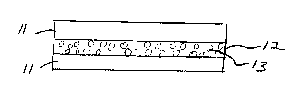
Figure l refers to a cross section of two magnetic
alloy strips bonded together.
Figure 2 is a cross section o~ a stack of bonded
magnetic alloy strips,
Detailed Description of the Invention
As used in the specifications and claims herein, the
term "interlayer or interlaminar -~horting" refers to
contact between a magnetic alloy strip and a different
magnetic alloy strip. This contact results in electrical
current running between the layers. This electrical
current, eddy current, re~uces the e~ficiency of the
lam~nant core.
2 1 ~
~s used in the specification and claims, "stacking
factor" refers to the ratio of actual magnetic material
present in each stacked core to a core composed only of
magnetic 7~aterial ~e.g., ~olid). ASTM D-71B describes the
S proaedure ~or deter~ining ~he stacking ~actoriof the core.
The magnetic alloy strips used in the present
invention are uncoated. The magnetic alloy strips are
ge~erally available commercially as-rollad and annealed
stock with a corrosion preventing oil coating and vapor
barrier seal. The magnetic alloy strips are often referred
to as transformer stock. The magnetic alloy strips include
silicon steel alloy, nickel steel alloy, and valadium
permadur. A particularly useful magnetic alloy strip
comprises a silicon steel alloy strip, pre~erably a silicon
steel alloy strip having up to 9% by weight, more
preferably up to about 6% by weight silicon. The magnetic
alloy strips generally have a thickness less than about
0.51 ~n (0.02 inches).
A bond layer is placed between the uncoated, magnetic
alloy strips. The bond layer includes a particular filler
having an averaqe particle size su~ficient to prevent
interlayer shorting of the magnetic alloy strips. In one
embodiment the particle ~iller has an average particle size
from about 0.5, or about 0.9, or about 1.0 . The particle
size of the filler may be up to abo7~t 8, or to about 7, or
to about 6 microns. In one embodiment the particulate
filler has a median partiGle si~e fro~ about 0.5, or about
0,9 or about 1 up to about 2, or to about 1.8, or to about
1.6, or to about 1.4 micron~. In another e7nbodiment the
particulate ~iller has a mean particle size from about 0.5,
or about 1, or about 2 up to about 8, or to about, or to
about 6 microns. The mean particle size is determined by
the Malvern 3600 Particle Size Analyzer. The particulate
~0~
filler has a narrow particle distribution. In one
embodiment, the particulate filler has a particle size
distribution by vol~me of 100% less than about 20 microns,
or about 99.9% less than about 15 microns, and or about
97.2~ less than about 11 microns. --
The particulate fillers are generally used at a level
~rom about 5%, or about 7%, ox about 9% up to about 25~, or
to about 18%, or to about 16%, or about 14% by weight of
the adhesive and particulate filler. In one embodiment, the
partlculate filler is used with an inorganic binder. In
this embodiment, the particulate filler is generally
present in an amount from about 9~, or about 12% up to
about 25%, or to about 22%, or to about 20% by weight of
the inorganic binder and particulate filler.
The particulate filler may be any non-conductive
filler having a particle size, axi described herein.
Examples of particulate fillers include ceramic
microspheres, and chopped glass fibers. In one embodimint,
the particulate filler compri~es a ceramic microsphere, and
especially a hollow, thick-walled, silica-alumina alloy
microsphere. An example of this ceramic microsphere is
Zeeospheres~ fillers available commercially from 3M
Chemical Company. A particularly useful .ceramic
microsphere is Zeeosphere~ 200. Zeeosphere~ 200 is
characteri~ed as having a median particle ~ize of 1.3
microns; a mean particle size of a particle size of 5.3
microns; a distribution by volume of 90% less than 9.0
microns, 50~ less than 5.1 microns, and 10% less than 2.2
microns. The residual weight percent retained on a 325
mesh (45 micron) screen is 0.01% ~determined by ASTM D-
1~5~.
2 ~
The particulate fill~r i~ combined with an adhesive to
form the ~ond layer (B). The bond layer, or bondline,
generally has a thickness ~rom about 3, or about 5, or
about 7 up to about 25, or about 20, or about 15 microns.
S The bond layer is ~general~ *hi~ik enough ~to provid~
electrical insulation b~bwe~n the,~gnetic alloy ætrips but
thin enough to provide optimal stacking factor. I
As described above, the bond layer also includes a
cured adhesive. The adhesive may be phenolic, silicon
rubber or an epoxy adhesive. Generally, epoxy adhesives
are preferred. Epoxy adhesives are generally diglycidyl
ethers of bisphenol A derived fxom bisphenol A and
epichlorohydrin. One way of preparing epoxy resins is a
two part adhesive package. The first part contains a
dichlorohydrin of bisphenol A. The other part contains a
curing agent. Curing agents include anhydrides, ~mines,
polyamines, Lewis acids, etc. Important classes of curing
agents include polyamines, polyaminoamides tformed from
polyamines and dimerized fatty acids e.g., acids containing
1 to 30 carbon atoms~, polyphenols, polymeric thiols,
polycarboxylic acids, and anhydrides. An example of a
seful epoxy adhesive is Bondma-Rter E645 adhesive,
available commercially from National S~arch and Chemical
Company.
In another embodiment, the binder composition also
includes a cured inorganic binder. The inorganic bindi~r
together with the particulate filler form an inorganic bond
layer between the uncoated, magnetic alloy steel strips.
An example of a useful inorganic binder is Cerama-bind~
binder available commercially from Aremco Products Inc. A
particularly useful inorganic binder is Cerama-bind~ 644.
:.
' ' '. :
2 1 ~
The invention is further exemplified with reference to
the drawings. .In ~i~ure 1, ~agnetic alloy strips 11 are
bonded together with bonding layer 12. Bonding layer 12
has particulate matter 13 disper~ed within the bonding
layer. -~
In figure 2, the stack is compo ed of magnetic alloy
strip layers 21 having bonding layers 22 between each layer
of magnetic alloy strip.
The invention also relates to a method o~ preparing an
electrical laminant comprising the steps of ~1) coating a
magnet.ic alloy strip with a binding composition including
a particulate ~iller having an average particle size
sufficient to prevent interlaminar shorting, t2) forming a
stack of coated magnetic alloy strips, (3) applying pres-
sure to the stack, and (4) curing the binding composition.
In another ambodiment, the invention also relates to a
method of preparing an electrical laminant comprising the
steps of (1) forming a stack of uncoated, magnetic alloy
strips, (2) coatiny tha magnetic alloy strips with a
binding composition including a particulate *iller having
an average particle size sufficient to prevent interlaminar
shorting, (3) applying pressure to the stack, and (4)
curing the binding composition.
Generally, the uncoated, magnetic alloy ~trips are
cleaned and degreased. Cleaning is generally accomplished
by using methyl ethyl ketone or any degreasing solvent.
The magnetic alloy strips are then coated with a binding
composition. The amount of time between degre.asing and
coating should be ~inimized to prevent rusting of the
magnetic alloy stripsO The magnetic alloy Rtrips may be
coated by any means known to those in the art, such as
painting, spraying, dip coating, etc.
` '
. . .. : . ., ~ , .. .
2 1 ~
In one embodi~ent, the ma~netic alloy strips are
vacuum impregnated with the binding composition.
Generally, the individual cleaned, uncoated ~agnetic alloy
strips, or a stack (loosely bound) of uncoated, magnetic
alloy strip~ are placed under~vacuum in a ~uitable vessel.
The vessel ~s then fl~oded with -the binding composition.
The magnetic alloy strips, or stacks thereof generally
remain in the binding composition for about 15-30 minutes.
Vacuum is released and excess binding composition is
drained from the individual strips or stack. The vacuum
~enerally acts to prevent inclusion o~ air bub~les in the
coating of the individual alloy strips or stacks. The
vacuum is generally below about 100 mm Hg, or below about
50 mm Hg. A vacuum of 20-30 ~m Hg is particularly usePul.
In another embodiment, individual magnetic alloy
strips are placed in the suitable vessel. A vacuum is
pulled on the vessel and the strips are dipped into a
binding composition. The vacuum is released and the strips
are removed from the binding composition and dried.
In the present invention, the coated magnetic alloy
strip~ are formed int~ a stack as is known to those in the
art. The exact ~tacking arrangement is not critical to the
pre~ent invention. After the individual alloy strips have
been coated and formed into a stack or coated as a stack,
pressure is applied to the stack. Pressure can be applied
by any means known to tho~e skilled in the art, such as by
applying spring pressure. The pressure is generally from
about 4,500, or about 6,000, or about 9,000, up to about
20,000, or about 18,000 newtons (from about 1,000 to about
4,400 pounds).
2 ~
The binding composition is cured while maintaining
pressure on the stack. ~uring generally occurs at a
temperature of about 65C, or abou~ 80C~ or about 125C up
to about 240CI or to about 200C (from about 150F to
5about 450~F)~ Generally,~thel curin~ occurs withi~ about
0.5, or about l hours u~o ~ou~l9~hours,~or to about 3
hours. The curing time begins after the stack has reached
curing temperatures. After curing the binding composi~ion
the stack is generally allowed to return to ambient
10temperatures and the pressure is released from the stack.
In another embodiment, invention relates to a composi- -
tion useful in binding electrical laminants comprising (i)
an epoxy adhesive and (ii) a hollow, thick-walled, silica-
15alumina alloy microsphere. The epoxy adhesive and silica-
alumina alloy microsphere have been described above.
: '
The following example relates to the articles,
methods, and compositions of the present invention. Unless
20otherwise indicated, as used in the examples as well as
elsewhere in the specification and claims, parts are parts
by weight, and temperatures is in degr~e celsius.
Exam~le
25A binding composition is prepared by mixing 45 parts
o~ Bondmaster E645 is added to 49 parts of methyl ethyl
ketone. Then, 6 parts of Ze~osphere~ 200 is added to the
mixture and blended until a uniform composition is ob-
tained. The viscosity of the mixture is 30 s~conds in a #1
30Zahn cup at room temp~rature.
Lamination surfaces of a transformer stock having
about 6% silicon, are cleaned and degreased using methyl
ethyl keton~. The binding composition above is sprayed on
35the lamination sur~ac~s to a dry film thickness o~ 12.5 to
,
2 1 ~
25 mm ~0.5 to 1 mill. Solvent is removed at about 65C for
lo to 60 minute~ in a forced air oven. The coated
lami~ants are stackad in a ~ixture. A clamping force of
4,500 to 18,000 newtons (1,000 - 4,000 pounds gage) is
applied to the stack by 6pring. The clamped stack is
placed in a forced air oven at 175e for 2 hours. The two
hours begin after the stac~ has reached oven temperature.
After two hours, the stack is removed and allowed to cool
to room temperature. After cooling to room temperature the
spring pressure is removed from the stack. The stack is
then removed and useable in a transformer, stator or rotor,
as known to those in the art.
.
Table_l
In Table 1, laminations ar~ made by the above
described procedure. Table 1 contains data comparing th~
effects of the binding com~ositions on stacking factor and
resistivity o~ uncoated, magn~tic alloy strips. Examples
1, 2, and 3 r~late to the present invention and include
particulate filler (Zeeosphere0 200) in the binding
compo~ition. Examples 4, 5, and 6 are co~parative examples
and relate to laminations made from bare ~ransformer stock
without the use of particulate filler. Examples 7, 8, and
g are comparative examples and relate to coated magnetic
alloy strips which are bound together by the epoxy
adhesive, Bondmaster E645.
2iO61 ~0
Tuble 1
_ ~_ ~ _ . . _ I
Ex. L~min~tion Filler Force Bond Ave. Surf~ce
~e~tcns) Thicknos~ St~cking Resistivity
L ~icrons~ F~etor ~AST ~718) ¦ . .
l Rare Yo6 4500 10.3 0.926 84.30 ¦
1---- - -- - ---- ------ - _ I
2 Baro Yes 9000 7.9 0.9U 7 S0 I .
~ _ ___ ~ .. I , .
3 Bare Yes 18,000 8.2 0.940 1.08 I .
I_ ~ _ _ __ _ I .... .
B~re ~one 4500 3.1 0.976 0.19
B~re ~on~ gO00 1.1 0.992 0.03
6 Bare None 18,000 0.4 0.997 0.03
7 Cost~d None 4500 2.1 0.938 9.53 ¦ .
_ . _ . . ._ _ _ .
0 8 Coated Uone 9000 2.8 0.934 7.69
9 Co~ted ~one 18,000 0.8 ' 0.948 1.75
= .-= i- == ~ .. -- ---=
As can be seen from the above table, stacks made with ~.
bare lamination and filler (Examples 1, 2, and 3) have :
lower dimensional variation and higher resistivity compared
to stacks made with bare laminations and no filler
(Examples 4, 5, and ~). Examples l, 2, and 3 have more
consistent stacking factor and bondline thickness at
different clamping forces. Examples 1, 2, and 3 show no :
bondline separation (delamination~. Applicants have
discovered that the use of a particulate filler leads to
lamination separation control which provides consistent
stack density, consistent stack height and ~inimized stack
shorting.
`` 2:1 06~
While the invention has been explained in relation to
its preferred embodiments, it is to be understood that
various modifications thereof will become apparent to those
skilled in the art upon reading the specifiaation.
S Therefore, it is to be unde~stood that the invention
disclosed herein is intended to cover ~uch ~odifications as
well as fall within the scope of the appéndant claim.
. - . - . . .. , , . - ,.. . . . . .. , : -: . ~ .. : .: . ... : : , . , : : : :
.. , .,: ,:; .,. -., . , . . : .. . : . , :~. .