Note: Descriptions are shown in the official language in which they were submitted.
CA 02106366 1999-12-22
1
ELECTRICAL PLUG CONNECTOR
The invention relates to an electrical plug
connector for telecommunication and data applications.
EP 0, 445, 376 A1 describes a plug connector having
a housing with a receiving chamber for the plug, a first
set of insulation displacement contacts and a second set of
contacts (RJ contacts) connected to the first set of
contacts. The RJ contacts are made of elongated contact
strips inserted into grooves of the upper housing portion
and guided closely to each other and parallely right into
the receiving chamber, whereinto an RJ plug can be
inserted. The contact strips are guided over longitudinal
parallel paths and at small distances from each other,
which results in a capacitance effect being generated
between the contact tracks, leading to poorer values of
crosstalk attenuation.
United States Patent Number 5,186,847
describes an electrical plug connector for
applications in the field of high-frequencies. The
electrical plug connector has parallel contact tracks which
are bent and disposed relative to each other such that a
portion of the contact tracks cross each other, thereby
reducing the values of crosstalk attenuation. However, the
required values for voice or data transmission over
transmission paths with 100 megabits/s or in the frequency
region of about 100 MHz, respectively are not guaranteed.
It is therefore the object of the invention to
provide an electrical plug connector for telecommunication
and data applications having substantially improved
electrical parameters and which satisfies the requirements
for transmission of high data rates.
According to one aspect of the present invention,
there is provided an electrical plug connector for
telecommunication and data applications, comprising RJ
contacts disposed in a housing, insulation displacement
CA 02106366 1999-12-22
2
contacts and contact strips connecting the RJ contacts and
the insulation displacement contacts, the contact strips
multiply and differently angled between the RJ contacts and
the insulation displacement contacts, and are, at least in
the area of a contact tongue, partially in different
planes.
According to another aspect of the present
invention, there is provided an electrical plug connector
for telecommunication and data applications, comprising RJ
contacts disposed in a housing, insulation displacement
contacts, contact strips connecting the RJ contacts and the
insulation displacement contacts, and means for affecting
the capacity disposed between the contact strips.
In accordance with the present invention, the
capacitive imbalance between contact arrangements is
considerably minimized.
In the accompanying drawings which illustrate
embodiments of the present invention:
Figure 1 is an exploded perspective view of a
plug connector described in EP 0,445,376 Al;
Figure 2 is the equivalent circuit for two
contact pairs of the plug connector of Figure l;
Figure 3 is a diagrammatical representation of
the line connections in the plug connector of Figure 1;
Figure 4 is an exploded perspective view of the
plug connector according to the present invention;
Figure 5 is a diagrammatical representation of
the line connections in the plug connector of Figure 4;
Figure 6 is an exploded perspective view of a
second embodiment of the plug connector according to the
present invention;
Figure 7 is an exploded perspective view of a
third embodiment of the plug connector according to the
present invention; and
CA 02106366 1999-12-22
3
Figure 8 is a bottom plan view of another
configuration of the connection elements according to the
present invention.
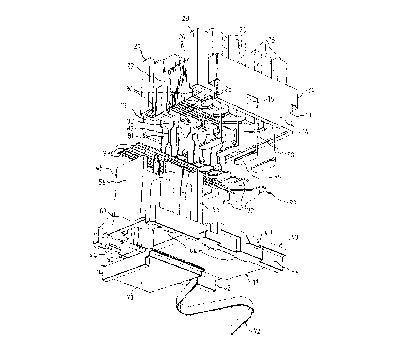
Referring now to Figure 1, a plug connector known
in the art from EP 0,445,376 comprises a moulded housing
having an upper housing portion 10 and a lower housing
portion 11. The upper housing portion 10 has opposing
substantially rectangular side walls 14, 15, each provided
with an opening 16 for latching a wedge-shaped projection
43 of the lower housing portion 11. Clamping elements are
formed by two rows of column-like extensions 18 which are
provided on the upper side of the upper housing portion 10
proximate the side walls 14, 15. Slots 20 are formed
between the extensions 18 to receive, as will be described
in more detail below, electrically conductive connection
elements 80 are integrally formed with angled, flat foot
sections 85. The front end wall 22 of the upper housing
portion 10 is provided with a row of parallel grooves 24 in
connection with similar grooves 26 formed in the lower wall
of the upper housing portion 10. Each of the grooves 26
extends proximate the lower part of a slot 20 defined by
the column-type extensions 18. The front end wall 22
further comprises opposing moulded and angled flange side
portions 28, 29, each of which form a channel 30. On the
end wall opposite the front end wall 22, the upper housing
portion 10 is provided with integrated hooks 34 forming
clamping elements for electrical conductors.
The lower housing portion 11 is provided with a
substantially flat end section 40 having opposing side
walls 42, the outside surfaces of which are provided with
wedge-like projections 43. The inner side of each side
wall 42 is provided with inwardly directed flanges 44. The
front end portion 45 of the lower housing portion 11
includes a moulded portion defining a hollow space 50 for
receiving a plug, such as a plug disposed at the tail end
of a cord coming from a telephone set or a computer
CA 02106366 1999-12-22
4
terminal. Opposing upright columns 56 are formed close to
the flat end section 40, approximately in the centre of the
lower housing portion 11. The lower housing portion 11
comprises a planar wall 58 extending upwardly at the front
end of the lower housing portion 11 to a height
approximately equal to the height of the columns 56. The
other end of the planar wall 58 terminates at projecting
portions 60 of each of the side walls 42. The lower
housing portion 11 may receive a closure cover 70 which is
disposed between the opposing side walls 42 and held in
position by the flanges 44. The closure cover 70 may be
displaced between a position wherein access to the hollow
space 50 is blocked and a position wherein the hollow space
50 is open. A spring 72 is attached at the closure cover
70 to bias the closure cover 70 towards the closed
position.
A set of eight electrical connection elements 80
extend into the slots 20 formed by the column extensions 18
in the upper housing portion 10. Each of the connection
elements 80 is provided with a fork-shaped insulation
displacement contact element 81 defining a relatively
narrow contact slot 82 terminating in a wide insertion
section 83. The arrangement is adapted such that, when
inserting an electrically insulated conductor into the
insertion section 83, and when pressing the conductor into
the narrow contact slot 82, the insulation of the conductor
will automatically be cut so that contact between the
central core of the conductor and the material of the
connection element 80 will be established. The insulation
displacement contact elements 81 are substantially flat and
are disposed at an angle of approximately 45° to a line
through the column-like extensions 18, i.e. at 45° to the
plane of each slot 20. Each connection element 80 is
further provided with a foot section 85 integrally formed
with the insulation displacement contact elements 81.
CA 02106366 1999-12-22
A second set of connection elements 90 comprise
a row of eight contact tongues 92, each of which is welded
to a foot section 85. An elongated contact strip 93
extends from each contact tongue 92. The contact strips 93
5 are adapted such that they extend in parallel relation to
each other. The contact strips 93 terminate as RJ contacts
in a receiving portion for the RJ plugs of terminals (not
shown in detail) .
The prior art plug connector can be considered as
a 8-wire/4-pair plug connector, including eight contacts
which can be represented, for example, in the following
configuration, as shown in Figures 1, 2 and 3:
Wires/contacts Pair configuration
1 and 2 pair 2
3 and 6 pair 3
5 and 4 pair 1
7 and 8 pair 4
The eight contacts shown at position 120 in
Figure 3 are RJ contacts and establish contact with the
contact strips 93 in a plug situated in the hollow space
50. The contact strips 93 extend in parallel relation to
each other up to the connection elements 80 adapted as
insulation displacement contact elements 81.
An analysis of this arrangement yields a
simplistic mathematical model wherein the contact pairs can
be regarded as a bridge circuit. The respective equivalent
circuit, for example, for pairs 1 and 3, is shown in Figure
2, wherein:
C1 represents the capacitance between contacts 3 and 5;
C2 represents the capacitance between contacts 3 and 4;
C3 represents the capacitance between contacts 5 and 6;
C4 represents the capacitance between contacts 6 and 4;
and
R1 represents the line impedance.
When the capacitance C1 between contacts 3 and 5
(Figure 2) is defined as 1, the capacitances C2 and C3 are
CA 02106366 1999-12-22
6
each of the amount 2, and the capacitance C4 is also of the
amount 1 (Figure 2).
To avoid crosstalk, current must not f low through
resistor R1, i.e. the bridge shown in Figure 2 must be
balanced. This, in turn, requires fulfilment of the
condition.
C1 C3
C2 C4
However, if the bridge comprises, as shown in the
example, capacitance values of 1 for C1 and C4 and
capacitance values of 2 for C2 and C3, then the bridge is
distinctly imbalanced. This situation exists between pairs
1 and 3 as well as between pairs 2 and 3 and pairs 3 and 4.
The main reason for crosstalk is the capacitive imbalance
between the pairs.
Crosstalk can be minimized, when the RJ contacts
of a plug connector are adapted such that the capacitive
imbalance is reduced, or elements are brought into
connection with the contacts, which provide a controlled
capacity thereby reducing the imbalance. The RJ contact
arrangements can be organized so that not only the internal
capacitive imbalance, but also the internal capacitive
imbalance of each assigned, suitable plug is compensated.
The plug connector according to the invention
shown in Figure 4 corresponds in its construction, to the
housing of the plug connector according to Figure 1 formed
of an upper housing portion 10 and of a lower housing
portion 11. The contact strips 93 are adapted, however,
such that they do not extend in parallel relation to each
other, on a portion of their path, but are disposed in
multiply angled paths from the hollow space 50 to the
connection elements 80 or to the contact tongues 92,
respectively. The contact tongues 92 are disposed in one
plane. From the plane of the contact tongues 92, the
contact strips 93 are in part multiply angled, in the area
of the contact tongues 92, towards the top, bottom left
CA 02106366 1999-12-22
7
and/or right, and in part cross each other. The RJ contact
1, for example, is connected over its contact strip 93.1
with the contact tongue 92.2, the RJ contact 2 is connected
over its contact strip 93.2 with the contact tongue 92.1,
the RJ contact 3 is connected over its contact strip 93.3
with the contact tongue 92.3, the RJ contact 4 is connected
over its contact strip 93.4 with the contact tongue 92.5,
the RJ contact 5 is connected over its contact strip 93.5
with the contact tongue 92.4, the RJ contact 6 is connected
over its contact strip 93.6 with the contact tongue 92.6,
the RJ contact 7 is connected over its contact strip 93.7
with the contact tongue 92.8, and the RJ contact 8 is
connected over its contact strip 93.8 with the contact
tongue 92.7.
Figure 5 demonstrates that, by such arrangement
of the contact strips 93, the capacity Cl between contacts
3 and 5 and the capacity between the RJ contacts 6 and 4 is
increased, since the RJ contacts are closer together.
Accordingly, a compensation of the capacities is achieved.
Such compensation can also be achieved by a reduction of
capacities C2 and C3, by positioning the RJ contact
elements 3 and 4 further away from each other. The
electrical parameters of the remaining configuration pairs
can also be affected.
A second embodiment of the present invention is
shown in Figure 6, wherein the housing is not depicted.
The contact strips 93 are angled in a different manner, and
are then guided in parallel relation to each other.
Figure 7 shows a third embodiment of the
connection elements 90 and the contact tongues 92 according
to Figure 4. A second contact element 95 is connected to
the connection elements 90 and the contact tongues 92. The
second contact element 95 can either be a printed circuit
board or a metal element, such element being insulated with
a high-dielectrical material. Such high-dielectrical
material is positioned in certain regions on the contact
CA 02106366 1999-12-22
8
element 95, in order to provide a controlled capacity to
the remaining contact positions and to compensate the
internal capacitive imbalance.
Another embodiment of the connection between the
contact tongues 92 and the contact strips 93 is shown in
Figure 8. In this embodiment, the contact strips 93
partially cross each other in the area of the connection to
the contact tongues 92. The contact strip 93.1 is guided
to the contact tongue 92.2 and crosses the contact strip
93.2 being guided to the contact tongue 92.1. The contact
strip 93.3 is guided to the contact tongue 92.3 without
crossing. The contact strip 93.4 is connected with the
contact tongue 92.5 and crosses the connection between the
contact strip 93.5 and the contact tongue 92.4. The
contact strip 93.6 is connected with the contact tongue
92.6. The contact strip 93.7 is guided to the contact
tongue 92.8 and is crossed by the connection between the
contact strip 93.8 and the contact tongue 92.7. The
contact strips 93 and the contact tongues 92 are disposed
in the plug connector area in guide webs 57 of the lower
housing portion 11. The guide webs 57 have interruptions
59 in the crossing area of the contact strips 93. The
contact strips 93 and the contact tongues 92 are disposed
in two planes at the crossing positions only, but are
generally in one plane. The partially crossing contact
strips 93 guided in plastic guide webs 57 effect a
reduction of the mutual capacitive influences.