Note: Descriptions are shown in the official language in which they were submitted.
1 190
- CROSS-REFERENCES TO RELATED PATENTS
2 ~ 07 1 90
U.S. Patent No. 5,157,441, issued October 20, 1992 in the
name of Scheuer et al and assigned to the same assignee as the instant
application relates to a single pass tri-level imaging apparatus and
method. Compensation for the effects of dark decay on the
background voltage, VMOd~ and the color toner patch, Vtc readings is
provided using two ESVs (ESV, and ESV2), the former located prior to
the color or DAD housing and the latter after it. Since the CAD and
black toner patch voltages are measured (using ESV2) after dark decay
and CAD voltage loss have occurred, no compensation for these
readings is required. The DAD image voltage suffers little dark decay
change over the life of the photoreceptor so the average dark decay
can be built into the voltage target.
U.S. Patent No. 5,212,029 issued May 18, 1993 in the name of
Scheuer et al and assigned to the same assignee as the instant
application relates to toner patch generation for use in tri-level imaging
which is effected using a laser ROS. Two toner patches are formed
using a single toner patch generator of the type commonly used in the
prior art. The patch generator, used by itself serves to form one toner
patch latent image and together with the ROS exposure device of the
imaging apparatus is used to form the other toner patch latent image.
Canadian Patent Application 2,076,791, published March 6,
1993 in the name of Scheuer et al and assigned to the same assignee
as the instant application relates to a pair of Electrostatic Voltmeters
(ESV) which are utilized to control the photoreceptor charging voltage
in a Tri-Level imaging apparatus. One of the ESVs is used to control
the voltage increases of a charging device. The other ESV is used to
monitor the charge level of the charged area image of a Tri-Level image.
When a critical value is sensed the control of the charging device is
shifted to the ESV that monitors the charged area image level and limits
the output from the charging device to a predetermined target value.
~A ~
2 ~ 0 7 1 90
U.S. Patent No. 5,227,270 issued July 13, 1993 in
the name of Scheuer et al and assigned to the same assignee as the instant
application relates to a single pass tri-level imaging apparatus, wherein a
pair of Electrostatic Voltmeters (ESV) are utilized to monitor various control
patch voltages to allow for feedback control of Infra-Red Densitometer
(IRD) readings.
The ESV readings are used to adjust the IRD readings of each
toner patch. For the black toner patch, readings of an ESV positioned
bet~,veen tvvo developer housing structures are used to monitor the patch
voltage. If the voltage is above target (high development field) the IRD
reading is increased by an amount proportional to the voltage error. For
the color toner patch, readings using an ESV positioned upstream of the
developer housing structures and the dark decay projection to the color
housing are used to make a similar correction to the color toner patch IRD
readings (but opposite in sign because, for color, a lower voltage results in a
higher development field).
U.S. Patent No. 5,210,572, issued May 11, 1993 in the
name of MacDonald et al and assigned to the same assignee as the instant
application relates to toner dispensing rate adjustment wherein the Infra-
Red Densitometer (IRD) readings of developed toner patches in a tri-level
imaging apparatus are compared to target values stored in Nonvolatile
Memory (NVM) and are also compared to the previous IRD reading. Toner
dispensing decisions (i.e. addition or reduction) are based on both
comparisons. In this manner, not only are IRD readings examined as to how
far the reading is from the target, they are examined as to current trend
(i.e. whether the reading is moving away from or toward the target).
U.S. Patent No. 5,223,897 issued June 29, 1993 in the
name of MacDonald et al and assigned to the same assignee as the instant
application relates to a tri-level imaging apparatus wherein two sets of
targets, one for use during cycle up convergence of electrostatics and one
during runtime enable single pass cleaning of developed patches, during
cycle up convergence. To this end, different targets from those used during
.A
21 071 90
runtime are used for the preclean, transfer and pretransfer dicorotrons
during cycle up.
Proper charging of the photoreceptor during runtime and cycle
up convergence is also enabled by the provision of two charging targets,
one for each mode of operation.
U.S. Patent No. 5,208,632 issued May 4, 1993 in the
name of Hurvvitch et al and assigned to the same assignee as the instant
application relates to cycle up convergence of electrostatics in a tri-level
imaging apparatus wherein cycle up convergence is shortened through the
use of an image output terminal (IOT) resident image (on a pixel or control
board) to obtain charge, discharge and background voltage readings on
every pitch.
U.S. Patent No. 5,138,378 granted to MacDonald et al on 8/11/92
relates to recalculation of electrostatic target values in a tri-level imaging
apparatus to extend the useful life of the photoreceptor. The increase in
residual voltage due to Photoreceptor aging which would normally
necessitate photoreceptor disposal is obviated by resetting the target
voltage for the full ROS exposure when it reaches its exposure limit with
current photoreceptor conditions. All contrast voltage targets are then
recalculated based on this new target.
The new targets are calculated based on current capability of the
overall system and the latitude is based on voltage instead of exposure.
U.S. Patent No. 5,236,795 issued August 17, 1993 in
the name of Berman et al and assigned to the same assignee as the instant
application relates to the use of Infra-Red Densitometer (IRD) readings to
check the efficiency of two-pass cleaning of the black toner patch in a tri-
level imaging apparatus. The IRD examines the background patch of the
tri-level image and declares a machine fault if excessive toner is detected.
U.S. Patent No. 5,132,730 granted to Hurwitch et al on 07121/92
relates to a single pass, tri-level imaging apparatus, machine cycle down
which is initiated when the color developer housing is functioning
improperly. The voltage level of the color image prior to its development is
read using an electrostatic voltmeter (ESV). The voltage level thereof is also
L/i
2~ 071 90
read after development The difference between these two readings is
compared to an arbitrary target value and a machine cycle down is initiated
if the difference is greater than the target.
U.S. Patent No. 5,119,131 granted to Paolini et al on 06/02/92
relates to a single pass, tri-level imaging apparatus, wherein erroneous
voltage readings of an Electrostatic Voltmeter (ESV) which has become
contaminated by charged particles (i.e. toner) are negated by using two
ESVs.
During each cycle up following a normal cycle down, a pair of
Electrostatic Voltmeters (ESVs) are utilized to measure the voltage level on
a portion of relatively uncharged portion of a photoreceptor. Using one of
the ESVs, which is less prone to contamination, as a reference, the zero
offset of the other is adjusted to achieve the same residual photoreceptor
voltage reading. The difference in the readings which is due to toner
contamination is the zero offset between the two ESVs. The offset is used
to adjust all subsequent voltage readings of the ESV until a new offset is
measured.
While the '131 patent addresses the problem of erroneous
voltage readings of electrostatic voltmeters used in a xerographic imaging
process, the solution disclosed therein assumes a toner-free reference ESV.
Ignoring the contamination of the reference ESV results in improper
development and cleaning fields during development.
Accordingly, it is an object of an aspect of the present
invention to provide a tri-level imaging system which does not ignore
the adverse affects of contamination of a reference ESV that has
become contaminated with toner.
It is an object of an aspect of the present invention to
adjust the developer housing biases to reflect particle contamination of
ESVs.
It is an object of an aspect of the present invention to
adjust the developer biases by an amount equal to the difference
between a reference voltage applied to the ground plane of a
photoreceptor and the reading of a reference ESV.
.. ,
2107190
BACKGROUND OF THE INVENTION
This invention relates generally to highlight color imaging and
more particularly to the formation of tri-level highlight color images in a
single pass.
The invention can be utilized in the art of xerography or in the
printing arts. In the practice of conventional xerography, it is the general
procedure to form electrostatic latent images on a xerographic surface by
first uniformly charging a photoreceptor. The photoreceptor comprises a
charge retentive surface. The charge is selectively dissipated in accordance
with a pattern of activating radiation corresponding to original images.
The selective dissipation of the charge leaves a latent charge pattern on the
imaging surface corresponding to the areas not exposed by radiation.
This charge pattern is made visible by developing it with toner.
The toner is generally a colored powder which adheres to the charge
pattern by electrostatic attraction.
The developed image is then fixed to the imaging surface or is
transferred to a receiving substrate such as plain paper to which it is fixed
by suitable fusing techniques.
The concept of tri-level, highlight color xerography is described
in U.S. Patent No. 4,078,929 issued in the name of Gundlach. The patent to
Gundlach teaches the use of tri-level xerography as a means to achieve
single-pass highlight color imaging. As disclosed therein the charge pattern
is developed with toner particles of first and second colors. The toner
particles of one of the colors are positively charged and the toner particles
of the other color are negatively charged. In one embodiment, the toner
particles are supplied by a developer which comprises a mixture of
tribocl~l,ically relatively positive and relatively negative carrier beads. The
carrier beads support, respectively, the relatively negative and relatively
positive toner particles. Such a developer is generally supplied to the charge
pattern by cascading it across the imaging surface supporting the charge
pattern. In another embodiment, the toner particles are presented to the
charge pattern by a pair of magnetic brushes. Each brush supplies a toner
of one color and one charge. In yet another embodiment, the development
2107190
systems are biased to about the background voltage. Such biasing results in
a developed image of improved color sharpness.
In highlight color xerography as taught by Gundlach, the
xerographic contrast on the charge retentive surface or photoreceptor is
divided into three levels, rather than two levels as is the case in
conventional xerography. The photoreceptor is charged, typically to 900 +
volts. It is exposed imagewise, such that one image corresponding to
charged image areas (which are subsequently developed by charged-area
development, i.e. CAD) stays at the full photoreceptor potential (VCAD or
Vddp). Vddp is the voltage on the photoreceptor due to the loss of voltage
while the photoreceptor remains charged in the absence of light, othervvise
known as dark decay. The other image is exposed to discharge the
photoreceptor to its residual potential, i.e. VDAD or Vc (typically -100 volts)
which corresponds to discharged area images that are subsequently
developed by discharged-area development (DAD) and the background
area is exposed such as to reduce the photoreceptor potential to halfvvay
between the VCAD and VDAD potentials, (typically -500 volts) and is referred
to as VWhite or Vw. The CAD developer is typically biased about 100 volts
closer to VCAD than Vwhite (about -600 volts), and the DAD developer
system is biased about -100 volts closer to VDAD than VWhite (about 400
volts). AS will be appreciated, the highlight color need not be a different
color but may have other distinguishing characteristics. For, example, one
toner may be magnetic and the other non-magnetic.
BRIEF SUMMARY OF THE INVENTION
Erroneous voltage readings of Electrostatic Voltmeter (ESVs),
which have become contaminated by charged particles (i.e. toner) from
developer housings used for developing latent images on a photoreceptor
surface, are negated by adjusting the readings of the ESVs to compensate
for the contamination of the ESVs. Additionally, the developer housing
biases are adjusted to insure proper development and cleaning fields
during development.
21 071 90
During each cycle up following a normal cycie down, the DC bias
from one of the developer housings is routed to the ground plane of the
photoreceptor for a brief period of time. Both ESVs read the voltage on the
photoreceptor which is equal to the the combination of the developer
housing bias on the ground plane plus the residual voltage on the
photoreceptor. One of the pair of Electrostatic Voltmeters
(ESVs),therefore, ESVl is utilized to measure the voltage level on a portion
of the photoreceptor. This ESV is used as a reference and the zero offset of
the other ESV (ESV2) is adjusted to obtain the same reading. Additionally,
the DC voltage supply outputs for both the color and black developer
housings are adjusted by the difference between bias voltage output that
was placed on the the photoreceptor ground plane and the actual reading
of the reference ESV.
As a result of the foregoing adjustments to ESV2 and the
developer housing biases, the combined voltage reading due to residual
voltatge on the photoreceptor and any combination of charged particles
within the probe housing of the reference ESV (ESV~) is arbitrarily set to
zero. All other voltages are now established relative to the reference ESV.
Therefore, all of the systems electrostatic values are properly set with
respect to each other thereby maintaining proper development and
cleaning fields over the life of the machine.
Other aspects of this invention are as follows:
In a method of creating tri-level images on a charge retentive
surface during operation of a tri-level imaging apparatus, the steps
including:
moving said charge retentive surface past a plurality of process
stations including a charging station where said charge retentive surface is
uniformly charged, a plurality of developer structures for developing latent
images and an illumination station for discharging said charge retentive
surface;
applying electrical bias voltages to said developer structu res;
applying a reference voltage to an uncharged charge retentive
surface;
, ~
~, ~
using a first sensor, sensing the voltaglqevll o~ said charge
retentive surface and generating a first signal representative of said
voltage level;
using a second sensor, sensing the voltage level of said charge
retentive surface and generating a second signal representative of said
voltage level;
using one of said senors as a reference, adjusting the zero offset
of the other of said sensors to achieve the same voltage reading as said one
of said sensors and generating a signal representative of the amount of
1 0 adjustment;
storing said signal representative of the amount of adjustment
in memory; and.
adjusting the electrical bias voltages applied to said developer
structures by an amount equal to the voltage difference between said
reference voltage applied to said uncharged charge retentive surface and
the voltage sensed by said reference sensor.
Apparatus for creating tri-level images on a charge retentive
surface during operation of a tri-level imaging apparatus, said apparatus
comprising:
means fo- applying electrical bias voltages to said developer
structures;
means for moving said charge retentive surface past a plurality
of processstations including a charging station where said charge retentive
surface is uniformly charged, a plurality of developer structures for
developing latent images and an illumination station for discharging said
charge retentive surface;
means for sensing the voltage level of a relatively uncharged
portion of said charge retentive surface and generating a first signal
representative of said voltage level;
means for sensing said relatively uncharged portion of said
charge retentive surface and generating a second signal representative of
said voltage level;
- 7a-
2t 071 90
means for adjusting the zero offset of the other of said sensors
to achieve the same voltage reading as said one of said sensors and
generating a signal representative of the amount of adjustment;
means for storing said signal representative of the amount of
adjustment in memory; and
means for adjusting the electrical bias voltages applied to said
developer structures by an amount equal to the voltage difference
between said reference voltage applied to said uncharged charge retentive
surface and the voltage sensed by said reference sensor .
DESCRIPTION OF THE DRAWINGS
Figure la is a plot of photoreceptor potential versus exposure
illustrating a tri-level electrostatic latent image;
Figure 1b is a plot of photoreceptor potential illustrating single-
pass, highlight color latent image characteristics;
Figure 2 is schematic illustration of a printing apparatus
incorporating the inventive features of the invention; and
Figure 3 a schematic of the xerographic process stations
including the anive members for image formation as well as the control
members operatively associated therewith of the printing apparatus
illustrated in Figure 2.
- 7b-
~.
2107190
Figure 4 is a block diagram illustrating the interaction among
active components of the xerographic process module and the control
devices utilized to control them.
DETAILED DESCRIPTION OF THE PREFERRED
EMBODIMENT OF THE INVENTION
For a better understanding of the concept of tri-level, highlight
color imaging, a description thereof will now be made with reference to
Figures 1a and lb. Figure 1a shows a Photolnduced Discharge Curve (PIDC)
for a tri-level electrostatic latent image according to the present invention.
Here Vo is the initial charge level, Vddp (VCAD) the dark discharge potential
(unexposed), Vw (VMOd) the white or background discharge level and Vc
(VDAD) the photoreceptor residual potential (full exposure using a three
level Raster Output Scanner, ROS). Nominal voltage values for VCAD, VMOd
and VDAD are, for example, 788, 423 and 123, respectively.
Color discrimination in the development of the electrostatic
latent image is achieved when passing the photoreceptor through two
developer housings in tandem or in a single pass by electrically biasing the
housings to voltages which are offset from the background voltage VMOd,
the direction of offset depending on the polarity or sign of toner in the
housing. One housing (for the sake of illustration, the second) contains
developer with black toner having triboelectric properties (positively
charged) such that the toner is driven to the most highly charged (Vddp)
areas of the latent image by the electrostatic field between the
photoreceptor and the development rolls biased at Vblack bias (Vbb) as
shown in Figure 1b. Conversely, the triboelectric charge (negative charge)
on the colored toner in the first housing is chosen so that the toner is urged
towards parts of the latent image at residual potential, VDAD by the
electrostatic field existing between the photoreceptor and the
development rolls in the first housing which are biased to Vcolor bias, (Vcb)
Nominal voltage levels for Vbb and Vcb are 641 and 294, respectively.
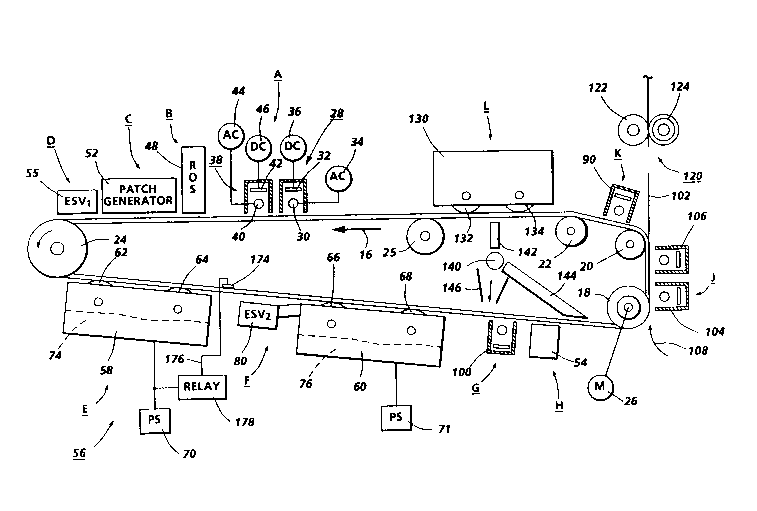
As shown in Figures 2 and 3, a highlight color printing apparatus
2 in which the invention may be utilized comprises a xerographic processor
2la7~s~
module 4, an ele~l-onics module 6, a paper handling module 8 and a user
interface (IC) 9. A charge retentive member in the form of an Active Matrix
(AMAT) photoreceptor belt 10 including a ground plane is mounted for
movement in an endless path past a charging station A, an exposure station
B, a test patch generator station C, a first Electrostatic Voltmeter (ESV)
station D, a developer station E, a second ESV station F within the developer
station E, a pretransfer station G, a toner patch reading station H where
developed toner patches are sensed, a transfer station J, a preclean station
K, cleaning station L and a fusing station M. Belt 10 moves in the direction
of arrow 16 to advance successive portions thereof sequentially through
the various processing stations disposed about the path of movement
thereof. Belt 10 is entrained about a plurality of rollers 18, 20, 22, 23 and
24, the former of which can be used as a drive roller and the latter of which
can be used to provide suitable tensioning of the photoreceptor belt 10.
Motor 26 rotates roller 18 to advance belt 10 in the direction of arrow 16.
Roller 18 is coupled to motor 26 by suitable means such as a belt drive, not
shown. The photoreceptor belt may comprise a flexible belt
photoreceptor. Typical belt photoreceptors are disclosed in U.S. Patent No.
4,588,667, U.S. Patent No.4,654,284 and U.S. Patent No.4,780,385.
As can be seen by further reference to Figures 2 and 3, initially
successive portions of belt 10 pass through charging station A. At charging
station A, a primary corona discharge device in the form of dicorotron
indicated generally by the reference numeral 28, charges the belt 10 to a
selectively high uniform negative potential, Vo. As noted above, the initial
charge decays to a dark decay discharge voltage, Vddp, (VCAD). The
dicorotron is a corona discharge device including a corona discharge
electrode 30 and a conductive shield 32 located adjacent the electrode. The
electrode is coated with relatively thick dielectric material. An AC voltage is
applied to the dielectrically coated electrode via power source 34 and a DC
voltage is applied to the shield 32 via a DC power supply 36. The delivery of
charge to the photoconductive surface is accomplished by means of a
displacement current or capacitative coupling through the dielectric
material. The flow of charge to the photoreceptor 10 is regulated by means
2107190
of the ~C bias applied to the dicorotron shield. In other words, the
photoreceptor will be charged to the voltage applied to the shield 32. For
further details of the dicorotron construction and operation, reference may
be had to US-A 4,086,650 granted to Davis et al on April 25,1978.
A feedback dicorotron 38 comprising a dielectrically coated
electrode 40 and a conductive shield 42 operatively interacts with the
dicorotron 28 to form an integrated charging device (ICD). An AC power
supply 44 is operatively connected to the electrode 40 and a DC power
supply 46 is operatively connected to the conductive shield 42.
Next, the charged portions of the photoreceptor surface are
advanced through exposure station B. At exposure station B, the uniformly
charged photoreceptor or charge retentive surface 10 is exposed to a laser
based input and/or output scanning device 48 which causes the charge
retentive surface to be discharged in accordance with the output from the
scanning device. Preferably the scanning device is a three level laser Raster
Output Scanner (ROS). Alternatively, the ROS could be replaced by a
conventional xerographic exposure device. The ROS comprises optics,
sensors, lasertube and resident control or pixel board.
The photoreceptor, which is initially charged to a voltage Vo,
undergoes dark decay to a level Vddp or VCAD equal to about -900 volts to
form CAD images. When exposed at the exposure station B it is discharged
to Vc or VDAD equal to about -100 volts to form a DAD image which is near
zero or ground potential in the highlight color (i.e. color other than black)
parts of the image. See Figure 1a. The photoreceptor is also discharged to
Vw or VmOd equal to approximately minus 500 volts in the background
(white) areas.
A patch generator 52 (Figures 3 and 4) in the form of a
conventional exposure device utilized for such purpose is positioned at the
patch generation station C. It serves to create toner test patches in the
interdocument zone which are used both in a developed and undeveloped
condition for controlling various process functions. An Infra-Red
densitometer (IRD) 54 is utilized to sense or measure the reflectance of test
patches after they have been developed.
-10-
2~ ~719~
After patch generation, the photoreceptor is moved through a
first ESV station D where an ESV (ESV1) 55 is positioned for sensing or
reading certain electrostatic charge levels (i. e. VDAD, VCAD, VMod, and Vtc)
on the photoreceptor prior to movement of these areas of the
photoreceptor moving through the development station E.
At development station E, a magnetic brush development
system, indicated generally by the reference numeral 56 advances
developer materials into contact with the electrostatic latent images on the
photoreceptor. The development system 56 comprises first and second
developer housing structures 58 and 60. Preferably, each magnetic brush
development housing includes a pair of magnetic brush developer roilers.
Thus, the housing 58 contains a pair of rollers 62, 64 while the housing 60
contains a pair of magnetic brush rollers 66, 68. Each pair of rollers
advances its respective developer material into contact with the latent
image. Appropriate developer biasing is accomplished via power supplies
70 and 71 electrically connected to respective developer housings 58 and
60. A pair of toner replenishment devices 72 and 73 (Figure 2) are provided
for replacing the toner as it is depleted from the developer housing
structures 58 and 60.
Color discrimination in the development of the electrostatic
latent image is achieved by passing the photoreceptor past the two
developer housings 58 and 60 in a single pass with the magnetic brush rolls
62, 64, 66 and 68 electrically biased to voltages which are offset from the
background voltage VMOd, the direction of offset depending on the
polarity of toner in the housing. One housing e.g. 58 ~for the sake of
illustration, the first) contains red conductive magnetic brush (CMB)
developer 74 having triboelectric properties (i. e. negative charge) such that
it is driven to the least highly charged areas at the potential VDAD of the
latent images by the electrostatic development field (VDAD - Vcolor bias)
between the photoreceptor and the development rolls 62, 64. These rolls
are biased using a chopped DC bias via power supply 70.
The triboelectric charge on conductive black magnetic brush
developer 76 in the second housing is chosen so that the black toner is
210719Q
urged towards the parts of the latent images at the most highly charged
potential VCAD by the electrostatic development field (VCAD - Vblack bias)
existing between the photoreceptor and the development rolls 66, 68.
These rolls, like the rolls 62, 64, are also biased using a chopped DC bias via
power supply 72. By chopped DC (CDC) bias is meant that the housing bias
applied to the developer housing is alternated betvveen two potentials,
one that represents roughly the normal bias for the DAD developer, ànd
the other that represents a bias that is considerably more negative than the
normal bias, the former being identified as Vsias ~ow and the latter as Vsias
High This alternation of the bias takes place in a periodic fashion at a given
frequency, with the period of each cycle divided up between the two bias
levels at a duty cycle of from 5-10 % (Percent of cycle at VBjas High) and 90-
95% at VBjas Low- In the case of the CAD image, the amplitude of both VBjas
Low and VBias High are about the same as for the DAD housing case, but the
waveform is inverted in the sense that the the bias on the CAD housing is at
VBias High for a duty cycle of 90-95%. Developer bias switching betvveen
VBias High and VBias Low iS effected automatically via the power supplies 70
and 74. For further details regarding CDC biasing, reference may be had to
U. S. Patent No. 5,080,988 granted to Germain et al on 1/14/92.
In contrast, in conventional tri-level imaging as noted above, the
CAD and DAD developer housing biases are set at a single value which is
offset from the background voltage by approximately -100 volts. During
image development, a single developer bias voltage is continuously applied
to each of the developer structures. Expressed differently, the bias for each
developer gructure has a duty cycle of 100%.
Because the composite image developed on the photoreceptor
consists of both positive and negative toner, a negative pretransfer
dicorotron member 100 at the pretransfer station G is provided to
condition the toner for effective transfer to a substrate using positive
corona discharge.
Subsequent to image development a sheet of support material
102 (Figure 3) is moved into contact with the toner image at transfer station
J. The sheet of support material is advanced to transfer station J by
2107190
conventional sheet feeding apparatus comprising a part of the paper
handling module 8. Preferably, the sheet feeding apparatus includes a feed
roll contaning the uppermost sheet of a stack copy sheets. The feed rolls
rotate so as to advance the uppermost sheet from stack into a chute which
directs the advancing sheet of support material into contact with
photoconductive surface of belt 10 in a timed sequence so that the toner
powder image developed thereon contacts the advancing sheet of support
material at transfer station J.
Transfer station J includes a transfer dicorotron 104 which sprays
positive ions onto the backside of sheet 102. This attracts the negatively
charged toner powder images from the belt 10 to sheet 102. A detack
dicorotron 106 is also provided for facilitating stripping of the sheets from
the belt 10.
After transfer, the sheet continues to move, in the direction of
arrow 108, onto a conveyor (not shown) which advances the sheet to fusing
station M. Fusing station M includes a fuser assembly, indicated generally
by the reference numeral 120, which permanently affixes the transferred
powder image to sheet 102. Preferably, fuser assembly 120 comprises a
heated fuser roller 122 and a backup roller 124. Sheet 102 passes between
fuser roller 122 and backup roller 124 with the toner powder image
contacting fuser roller 122. In this manner, the toner powder image is
permanently affixed to sheet 102 after it is allowed to cool. After fusing, a
chute, not shown, guides the advancing sheets 102 to a catch trays 126 and
128 (Figure 2), for subsequent removal from the printing machine by the
operator.
After the sheet of support material is separated from
photoconductive surface of belt 10, the residual toner particles carried by
the non-image areas on the photoconductive surface are removed
therefrom. These particles are removed at cleaning station L. A cleaning
housing 100 supports therewithin tvvo cleaning brushes 132,134 supported
for counter-rotation with respect to the other and each supported in
cleaning relationship with photoreceptor belt 10. Each brush 132, 134 is
generally cylindrical in shape, with a long axis arranged generally parallel
2107190
to photoreceptor belt 10, and transverse to photoreceptor movement
direction 16. Brushes 132,134 each have a large nurnber of insulative fibers
mounted on base, each base respectively journaled for rotation (driving
elements not shown). The brushes are typically detoned using a flicker bar
and the toner so removed is transported with air moved by a vacuum source
(not shown) through the gap between the housing and photoreceptor belt
10, through the insulative fibers and exhausted through a channel, not
shown. A typical brush rotation speed is 1300 rpm, and the
brush/photoreceptor interference is usually about 2 mm. Brushes 132, 134
beat against flicker bars (not shown) for the release of toner carried by the
brushes and for effecting suitable tribo charging of the brush fibers.
Subsequent to cleaning, a discharge lamp 140 floods the
photoconductive surface 10 with light to dissipate any residual negative
electrostatic charges remaining prior to the charging thereof for the
successive imaging cycles. To this end, a light pipe 142 is provided. Another
light pipe 144 serves to illuminate the backside of the photoreceptor
downstream of the pretransfer dicorotron 100. The photoreceptor is also
subjected to flood illumination from the lamp 140 via a light channel 146.
Figure 4 depicts the the interconnection among active
components of the xerographic process module 4 and the sensing or
measuring devices utilized to control them. As illustrated therein, ESV1,
ESV2 and IRD 54 are operatively connected to a control board 150 through
an analog to digital (A/D) converter 152. ESVl and ESV2 produce analog
readings in the range of 0 to 10 volts which are converted by Analog to
Digital (A/D) converter 152 to digital values in the range 0-255. Each bit
corresponds to 0.040 volts (10/255) which is equivalent to photoreceptor
voltages in the range 0- 1500 where one bit equals 5.88 volts (1500/255).
The digital values corresponding to the analog measurements
are processed in conjunction with a Non-Volatile Memory (NVM) 156 by
firmware forming a part of the control board 150. The digital values
arrived at are converted by a digital to analog (D/A) converter 158 for use in
controlling the ROS 48, dicorotrons 28, 54, 90, 100 and 104 and the power
supplies 70 and 71 for electrically biasing the developer structures 58 and
-14-
2107190
60. Toner dispensers 160 and 162 are controlled by the digital values.
Target values for use in setting and adjusting the operation of the active
machine components are stored in NVM.
Tri-level xerography requires fairly precise electrostatic control
at both development stations. This is accomplished by using ESV1 and ESV2
to measure voltage states on the photoreceptor in test patch areas written
in the interdocument zones between successive images. However, because
the color developer material reduces the magnitude of the black
development field in a somewhat variable manner, it is necessary to read
the electrostatics associated with the black development following the
color housing.
In such a system it is necessary that the ESVs are reasonably
precise in their readings. Although the ESVs can be calibrated to a common
source by a service representative, the ESV output is known to drift over
time if charged toner particles are deposited within the unit. A single ESV
cannot distinguish between charge on the photoreceptor and charge on a
toner particle sitting inside the ESV housing.
In the dual ESV control system such as disclosed herein, ESV1 is
taken as the reference for calibration purposes. At each cycle up following
a normal cycle down, the bias voltage output of one of the power supplies
70, 71 is routed to the photoreceptor ground plane connection 174 via
conductor 176 and a high voltage relay 178 operatively conected to the
electronic module 6. This output is applied for about 200 msec or just
enough time for the ESVl and ESV2 to read the voltage on the
photoreceptor. ESV2 is then adjusted to get the same reading as ESV1. The
adjustment of ESV2 in the foregoing manner will keep the ESV readings
precise with respect to each other. However, the development and
cleaning fields associated with the development systems S8 and 60 will not
be correct. This is because the bias voltages applied to the developer
housings have not been adjusted according to the ESV readings. Thus, in
addition to adjusting ESV2 to compensate for the offset between it and
ESV1, the DC bias voltage supply outputs for both the color and the black
developer housings are adjusted by the difference between the bias
-1 5-
210~190
voltage output routed to the photoreceptor ground plane and the actual
reading of the reference ESV, ESV1.
As a result of the foregoing adjustments to ESV2 and the
developer housing biases, the combined voltage reading due to residual
voltage on the photoreceptor and any combination of charged particles
within the probe housing of the reference ESV (ESV1) is arbitrarily set to set
to zero. All other voltages are now established relative to the reference
ESV. Therefore, all of the systems electrostatic values are properly set with
respect to each other thereby maintaining proper development and
cleaning fields over the life of the machine.
-1 6-