Note: Descriptions are shown in the official language in which they were submitted.
.~
210' 9'7 ~
BaCkal'_0- ynd o-the I~ EV~t~ ~w
Photovoltaic solar cells are semiconductor devices which
convert sunlight into electricity. solar calls based on crystal-
line silicon otter the advantage of high performance and stability.
The principle barrier to expanded utilization o! silicon Solar
ells for eloctric power .generation is the present high coat of the
solar cells.
tn conventional solar cells based on single crystal or
large grain polycrystalline silioon ingot processes, the major cost
!actor is determined by the requirement of sawing ingots into
walars. Sawing is an expensive processing step, and furthermore
results in the loss of approximately half the costly ingot material
ae silicon dust. The problea to be solved rscTuires the development
of a low-cost procasa, that efficiently employs low-coat materials
while ataintaining solar cell performance.
The technical requirements for a solution to the problem
are based on the achievement of a process that is controllable, has
high creel throughput, and generates material with adequate
crystalline aorphology . The prior art includes several
processes which either effectively achieve controlled grot~th, or
~igl~ ar~_al throughput of silicon shoat or ribbons. All these
approaches eliminate the eoatly process of sawing large areas to
create waters frog ingots. For example, publications by Iiopkins
(WEB), Ettouney, et al. tEF'G), Gurtler (RTR) and flyer, et al. (S8P)
describe processes that achieve controlled polycrystalline growth
oI grains greater than 1 mm in size at low linear speeds (and
2
0
21079'5
~nsaquently low areal generation rates). Common to these sheet
growth processes is th~ fact that the shoot pulling direction and
the direction of sheet growth are eolitaear All of these processes
oaploy a large temperature gradient (>50o degrees Cantigrado per
centimeter) along the sheet growth direction. This gradient is
necessary to achieve the practical linear speed indicated (typieal-
ly lees than ~ cm/minj, but also introduces largo thermal-induced
stresses. In many cases these stresses limit the practical sheet
width that can be achieved by causing sheet deformations which
asks solar cell lubrication untenable. Thermal stresses. can also
create crystalline defects which limit solar sell psrforx~anes.
Mach of these processes attempts to achieve grain silos that era as
large as possible in ord~sr to avoid the deleterious sffaats of
grain boutidariss on solar cell petformanas.
Ariothsr eat of processes has been developed that can
achieve high areal throughput rates. For exaztpla, publications by
Hates, et al. (i,hssj , Rslnreich, et al. (R~rFT) , Falckenbarg, et al.
(8-Web), Hide, st al. (CRP) and Lungs, et al. (R~GSj~ dsacrib~
proeossas that achieve polycrystalline sheet growth with gram
sizes in the 10 micron to 3 am range at high linear rates~(10 to
180o ca/ainj. Typically, th~se processes have difficulty maintain-
ing gsoastria control (width and thickness) (e.g. (?rAeB, R7~FT,
RGS) , and/or experience difficulty with contaurination o! the
silicon by the contacting materials (e. g. RAFT, S-web, CRpj.
Comaon to these sheet growth processes is the fact that the sheet
pulling direction and the direction of vrystallino growth in the
3
a.
210'~9'~5
sheet sra nearly perpendicular. It is this critical feature of
these proceseess that allows the simultaneous achievement of high
linear pulling speeds and reduced crystal growth speeds. Reduced
crystal growth speeds ere necessary for th~a achievement of
materials with high crystalline quality.
The prior art regarding the fabrication o! solar cells
frog polycrystalline materials raQuirss that the grain size be
greater than 1.0 ma.. This rsduirament on grain~size t~ras nacassi-
toted by the need to minimize the deleterious atfeats o! grain
boundaries evidsnt in prior art materials. Historically, small-
grained polycrystalline silicon (grain size less than 1.0 mss has
not bash a car~didat~ for phvtovoltaic saterial due to grain
boundary affects. Grain boundary reco~rbination lad to degradation
of voltage, currant and fill !actors in the solar sell. Previous
models, for exaaple Ghosh (1980] and Foesu~a (1980j, based on
racoatbination at active grain boundaries correctly predicted
performance of historical aatarials. By inference thaw modals
teach that the achievement of inactive grain boundaries peraits the
utilization o! seal! grained aatarials.
llilifY e! the =nvaa
It. is the object o= this inv~ntion to provide a low-cost
process for forming low stxess, col~.imnar-grained sheets that are
employed in high parlormanca solar cells.
further object o! this invention is to provide
tachnic~ues for manufacturing columnar-grained polycrystalline
4
2107975
silicon sheets for use as a substrate in solar coils,
overcomes the disadvantages of the prior art.
A yet iurthor object of this invention is to provide a
process for manufacturing a low-cost solar cell that employs small_
grained polycrystalline silicon with low-activity grain boundaries,
A still further object of thin invention is to provide a
substrate and a solar cell made from such process.
zn aaeordanee with thin invention the sheet is lorned by
using a columnar growth technique that controls the details of heat
flow, and thus growth speed of the poiyerystallin~ material. The
process begins with granular silicon that is applied to a setter
material; the setter and silicon are thon subjected to a designed
thermal sequence which results in the formation of a columnar-grai-
ned polycrystalline a~;licon rheet at high cereal throughput rates.
Ths equipment saployed to accomplish the process includes a lfne
source of energy and a polycrystalline sheet growth and annealing
technology.
Ice accordance with this invention the sheet is
formed by using a columnar growth technique that
controls the details of heat flow, sad thus growth
speed of the polycrystalline material. The process
begins with granular silicon that is applied to a
setter material; the setter sad silicon are then
subjected to a designed thermal sequence which results
is the formation of a columnar-grained polycrystalline
~silicoa sheet at high cereal throughput rates. The
r ~' ' 5
~ 107875
equipment ea~loyed to accomplish the process includes a
line source of energy and a polycrystalline sheet
gr~th and annealing techaology. The invention may
also be practiced with a process which includes a more
distributed source of energy application than a lane
source, such as by graphite-base infrared heating.
~ha Drayibe=
The single p=GV~ illustrates a per~tive view aboating
the sequence to~ fabricating low strsss, aoluanar-grained silicon
ahaats usable as avlar cells substrates ~.n accordance. with this
invention.
The present invexrtion is directed tv ttehui~GS used for
making improve8 columnar grain polycs-ystal~rina sheets which are
so
~. t-
,_.
.~ ~ ,
210'975
particularly adaptable for use as substrates or watore in so
far
cells. The ability to use the sheet as a solar cell substrate
makes possible the provision of a solar cell consisting entirely of
Silicon material where the sheet would lunetion as a substrate made
o! silicon and the remaining layers of the solar cell would also be
side o! silicon.
Tire desired propertiu o! the oolumnar-grained ailicoa
sheet or substrate fabricated for inclusion in a iow-cost solar
cell in accordance with the teachings of this invention are;
flatness, a smooth ~urlacs, minority carrier diffusion lan~gth
greater than ~p microns, minimum grain dimension at least two timaS
the,minority carrier diffusion lsngta, low residual stress and
relatively inactive Qrain boundaries, Tho desired properties o! a
prOC~s8 =0r labrieating coluumar-grain silicon. material appropriate
for inclusion in a low-post solar cell in accordance wins the
teachings of this invention are; low thermal stress procedure,
controlled nucleation, high steal throughput, and maple process
oonttol.
The eritoria l~Or the øalu~a~.-~t.a~ . ~~icon material product
v! flatness and smoothness arc required to' aaha solar cell
rabrication tes;able. ~Ths requiremeats on diffusion length and
grain sire are to ~tiniaize recombination losses in the bulk and at
grain surfaces (i.s. grain boundaries), respectively. The
requirement or relatively inactive grain boundaries is to effect
the minimization of grain boundai-y recombination. The requirwaent
6
210' 9'~ 5
of low residual stress is to minimize mechanical breakage and to
maintain high minority carrier diffusion lengths.
The criteria for the columnar-grained silicon process of
a low thermal stress procedure is to effect minimization of bulk
crystalline defects. The requirement of controlled nucleation is
to affect the aehievsment of the required grain morphology and
size. The criteria for high aroal throughput and s3,mple process
control are to achieve low-cost and manufaaturability.
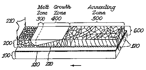
The single Figure is a perspective view illustrating the
sequence for fabricating low stress, columnar-grainv~d silicon
shuts. The process as depicted mouse frog left to right. In
general, a setter material loo, which sexvas as a mQCbanical
support, is coated with a granu3ar silicon layer Zoo, and is passed
through a presarfbed thermal profile. The prescribed thermal
profile first creates a melt region 300 at the top of the granular
silicon 200, end than creates a growth region 400 where both liquid
and a growing layer of polycrystalline layer coexist. Finally,
there is an a~ntiealing region So0 Where the temperature of the
polycrystalline silicon sheet layer 600 is ra~duaod in a prescribed
manner to affect stress relief.
The setter material 100 is selected based on the
following requiresents. It must: saintain its shape during the
sheet formation thermal proeassing; not chemically interact with,
or adhere to, the silicon material; and possess the proper thermal
characteristics tv effect the required sheet growth and annealing.
7
210'~9'~5
"~ S~veral materials including, but not limited to, quartz,
refractory boards (e.g. silica and/or alumina), graphite and
silicon carbide have been employed and maintained the proper
geometric shape during thermal processing.
To assure that the setter 100 does not adhere to the
final polycrystalline silicon sheet 600, a release agent coating
1i0 is applied to the setter. Either, or a combination of, silicon
nitride, silioon oxynitrida, silica or alumna have been employed
as this agent. 1~ low-coot method for applying this coating is to
fore a liquid slurry that is painted or sprayed on tho bare setter,
and than subsequsntly dried in an oxidizing atmosphere before use.
The release agont facilitates separation of the sheet and permits
reuse o! the setter material.
In the process design the thersal characteristics of the
settsr 100 play a key role in managing the melt and growth
processes. In the alt region 300 it is preferred that the thermal
conductivity of the setter be low to assure the efficient deploy-
ment of the energy, being used to pelt the grarniiar silicon 200.
The thermal properties of the setter may be tailored to possess a
strip of higher thormal conductivity under the outer edges X10 of
the strip of granular silicon. The effect of this strip is to
define the outer edges of the growing shoot. The tharmal.conduc-
tivity of the sett0r gay sees be tailored to assist in defining
nucleation sites to commence growth. This can be accomplished by
locally placing thermal shunts in the setter. These shunts provide
a thermal conduction path bstweea the top and bottom o! the setter,
8
210775
,,..., _
,:ftecting a local path for removing the h~at of aolidificativn, and
result in eitea where nucleated growth occurs.
In a preferred embodiment the setter material is low
density 1.5 cm thick 'ilica board. The s~ttar preparation is
completed by coating the top surface with a release agent ilo.
This is accomplished using an aqueous colloidal solution of silicon
nitrido that is painted on the top surface and baked in an
oxidi$ing at~sphers to form a non-wetting, non-adhorinq oxynitride
layer, before the initial application of granular silicon.
The granular silicon Z00 is saiectad based on the
following requirements. It must: be properly sizadj be of
adequate purity; and contain a chemical ingredient to provide a p-
typa resistivity of the grown silicon sheet 600 in the range of 0.1
to l0 ohm-cm.
The range of proper sizes for the granular silicon Z00
employed in the process is between 100 and 1000 micrometers. The
upper limit is detarminod by the design thickness for the silicon
sheet natarial. As a rule th~ minimua dimension of the largest
silicon particles should be ~l to or less than the desired
thickness of the silicon sheet :natarial. The lower size limit of
the particle distribution is dependant on the dynamics of. the
malting process, and the need to limit the amount of silicon oxide.
The silicon o~cida is a source o! sheet contamination, and naturally
occurs at all silicon surfaces.
The purity level necessary in the sheet silicon is
dater:ained by the raquirea:wnts for the efficient operation of a
9
ep"'v
solar csll device fabricated on the sheet. Whereas the eaployment
o! low-processing metallurgical grade silicon is not adequate,
utilization of highly processed semiconductor grade silicon is not
necessary. In practice the preferred process can be executed with
oft-grade semiconductor grade silicon. It is also an advantage o!
the preferred process that an additional degree of impurity
rsduction is acao~aplished during a~heet growth by segregation o!
3.mpurities to the sheet surtaaa, where they may easily be removed
by a subsequent chemical etch. This mechanism !or purirication by
segregation is operative in the preferred process as the actual
crystalline growth rata is less than 0.1 cm/min in the crystal
growth direction, comparable to that employed in the single crystal
float cone procsss. fihis maohanisn is not operative in sheaf
growth technologies that have the crystalline growth rate equal to
the echeet pulling apsad (approx., Z cm/min). At these higher
gro~rth velocities, there is not su!licient time !or effective
segregation to ooaur between liquid and solid~ar the process is
diffusion li~,tsd.
It is necessary to provide !or the addition o! a separate
constituent in, or with, the granular silicon to effect an
electrical roaistivity in the range o! 0.1 to 10 ohm-cm in the
sheet material. Typically, fox p-type conductivity in the cheat
material the preferred elements ors boron, aluminum or indium. As
an exaspls o! the preferred embodiment the addition o! powdsred
boron silicide followed by teechanical mixing o=. the granular
CA 02107975 1999-12-13
silicon provides for the accomplishment of the required p-type
resistivity in the subsequently grown silicon sheet.
The properly doped p-type granular silicon 200 ie
uniformly layered on the coated setter 10a. For example, this
process can be effectively accomplished by using a doctor blade.
The spacing between the edge of the doctor blade and the setter
surface needs to be at learnt ts~re times the mini~aum dimension of the
largest particle in the granular silicon size distribution.
Furthermore, the thicknesm of the final silicon sheet 600 can be as
little as the minimum dimension of the largest particle in the
granular size distribution. In a preferred
Qmbodiment a mixture of argoa and hydrogen gee is employed to
effectively limit the amount of oilicon oxide that is formed during
the growth process. The percent of hydrogen employed is determined
by the water vapor content in the chamber. The ratio of hydrogen
to water vapor controls the magnitude of silicon oxide formatio».
The vhamber may include a pre-heat zone employed to raise the
temperature to 1100 to 1400~C, which in combination with the
hydrogen present has the, effect o! reducing the native oxide og
silicon that exists on the granular silicon.
After the granular silicon 200 has been pre-heated it is
then brought into a thermal zone 3C0 where the top portion of the
granular silicon layer 200 is melted. In the preferred embodiment,
this thermal zone and the melting of the top portion of the layer
11
CA 02107975 1999-12-13
is accomplished using a focussed beam of light. The length or the
focussed beam along the direction of setter motion is about 1
centimeter. The depth of the granular silicon that is melted
depends on the intensity of the input energy from thermal zone 300,
the thickness of the granular silicon layer, the linear speed of
the granular silicon coated setter through thermal zone 300, and
the details of heat transfer between the granular silicon 200 and
the setter 100. .._
outor edges of the malt zone are stabilized by~the thermal shunts
engineered into the setter 100 or by reducing energy intensity at
the edges. These thermal shunts inhibit the depth of melting tit
the outer edges 210 and thus promote edge stabilization. Between
25 and 90~ (and preferably between 54t and 90~~ of the granular
silicon depth is melted. The material at the bottom of the
silicon d4pth io melted. The material at the bottom of the
granular layer is partially malted by liquid silicon penetrating
from the molten silicon layer above. This partially melted layer
of silicon forms a net 220. Other materials including fabrics that
are woven or non-woven, such as graphite, can be employed as the
net 2Z0. Other granular materialo that are partially malted or
unmelted, such as silicon carbide, can be employed as the net 220
material. The net 220 is responsible for four key process
features. First, because it wets to the molten silicon above, this
layer stabilizes the melt and growth zones by defeating the surface.
tension s~f the molten silicon over-layer. This allows the
production o! wide sheets, with smooth surfaces. Second, this
layer serves as a plane to nucleate subsequent growth. Third, this
12
2~.0'~9'~5
layer =inimizes molten silicon contact with the supporting setter
and release coating, thereby minimizing any potentia3 contamination
by impurities. Fourth, this layer serves ag highly defected back
plane, intrinsically gettering impurities from the active silicon
layer above, allowing the employment of lo~rer purity, lower-cost
grades of silicon raw material.
Where the net a20 is made lrcm a material ouch as
graphite, the graphite could be unrolled and applied over the
setter material before the granular silicon is applied. Thus, the
net is between the granular silicon and the setter material. The
later melted silicon would !unction as a nucleation site. The net
would lunation to stabilize the melt, ~ainisize molten silicon
contest with the underlying setter and act as a release coating.
Any or all of the preheat, meting, growth, and anneal thermal
profiles for the granular powder and resultant sheet could be achieved by
graphite based heater technology. _,
Jlfter leaving the melt creation zone.300 of the thermal
protilo, the welt pool on the partially melted silicon net 220
moves into the growth zone 400 of the theraal profile. 3n this
zone the growth is initiated on the silicon net ZZO. 8ecauae
growth is nucleated from the partially melted silicon net 2Z0, the
grain size o! the crranular silicon Zoo is an important parameter in
determining the size of the columnar grains in th~ grown sheet 600.
In the preferred onbodi~aent, mufti-grained or single crystal
granular silicon 200 is used to achieve relatively large columnar
grains (average grain size 0.2 to 1.0 xmj in the grown sheet 600.
13
2107975
In one embodiment, growth may also be preferentially initiated at
sites Z1o in the granular silicon layer where the heat transfer is
controlled by thermal shunting areas designed in the setter. The
direction of the growth front is approximately perpendicular to the
plane of the setter. The length of the growth Zone along the
direction of setter motion is from 2 to ZO centimeters, and is
slightly lees than the entire length of the melt pool. The length
of the growth Zone is determined by controlling the rata of loss o!
heat (and therefore growth rate) attending the eolidifiaation
process. As a consequence of the growth process, the grains that
are grown are columnar in nature. Typically, individual grains in
the r~aulting sheet 600 extend from the top surface to the bottom,
and are at least as wide as they are high. Sheet thicknes~es in
the range o= 400 to 500 aicrons can be achieved at ,sheet pulling
speeds in excus of 30 cmm/min.
After leaving the growth Zone 400 of the thermal profile,
the sheet 600 moves into the annealing Zone 500 of the thermal
profile. In this Zone the grown sheet, still at approximately
1400~G, is subjected to a linear teaperature gradient along the
direction o! setter motion. Ths linear temperature profile
eliminates buckliag and cracking of the as-grown sheet, and
nini~r!izes ~,..he generation of dislocations. The thickness of the
grown sheet is in the range of 350 to 1000 microns in the preferred
process. Because the thickness o! the final grown sheet so0 is
determined by the precise application of granular silicon Z00 to
the setter 100, exceptional sheet thickness control and process
14
,,-~ _ 2107975
stability are act~ievea in comparison to sheet technologies pulled
from a melt, where thickness is controlled by the melt meniscus.
After cool down, the sheet is removed from the setter, and
appropriately sized by sawing or scribing, for fabrication into
solar cells. The setter is reused !or making further columnar-
grained golyarystalline sheets.
The properties of tho sheet material fabricated with the
above process are quite amenable to the fabrication of efficient
solar sells. Tbis process generates material that has unique
properties o! rise and character. Although the grains are
columnar, and have average sizes in the range o= o.1 to l mm in
extant, solar calls fabricated on it may achieve voltages in excess
o! 560 x~V, and fill factors in excess of 0.7~. The achievement o!
thaae values on such small ~rainea natsrial indicate that _ this
material i~: not being limite8 by ~ecombiz,ation at grain ~ound-
aries as had been previously predicted by Ghoeh. Previously,
ooluanar grains were dismissed as being inoffictive since columnar
grains ware always small, aid small grains were thought not to
work. The process herein described achieves columnar grains that
yield aaterial with relatively benign grain bout~dariee xith the
result that sttiaiant, low-cost solar cells can be manufactured.
The process herein described can be carriod out in a
continuous marntr, resulting in continuous sheets that can be
appropriately sized using an in line scribe or a saw. Impurity
content in the melt and grown sheet quickly reaches steady-state;
it does not increase during continuous prooesaing. Since all
:5
.
~107~'~5
__
s~tbodisonts imcludo application of granular silicon to the setter,
and dines uatsrial enters the malt creation zone in this torn, malt
replenishment is not a problem, unlike sheet technologies pulled
from a malt pool. After being properly eiaad, tho shssts function
as a substrats by hawing the rsxaining layers fos~nsd tharoon to
produce solar calls. lihore the remaining layers are or silicon, a
complstoly silicon solar csli results.
16