Note: Descriptions are shown in the official language in which they were submitted.
210 8 ~18 LD0010265
- 1 -
HIGH-PRESSURE SODIUM LAMP CONTROL CIRCUIT
PROVIDING CONSTANT PEAK CURRENT AND COLOR
~'~', . ' ":
FIELD OF THE INVENTION
The present invention is directed to the operation of high-pressure - ~ -
sodium lamps. More particularly, the present invention is directed to a
high-pressure sodium lamp controi circuit which provides a constant peak
current through the lamp, thereby providing a constant lamp color. ~-
, .
BACKGROUND OF THE INVENTION
High-pressure sodium lamps are well known in the art and are
widely used for street, roadway and other outdoor lighting applications.
A high-pressure sodium lamp typically consists of a cylindrical transparent
or translucent arc tube which contains pressurized sodium vapor.
The arc tube generally has a pair of electrodes therein, and a -
current flows through the sodium vapor in the arc tube to excite the
sodium atoms. The current is preferably an ac current, which typically
offers an increased service life relative to a dc current. The energy which
is given off by the excitation and relaxation of the sodium ions is
.
' . '
2108418 LD0010265
- 2 -
converted into visible light and heat.
The arc tube is generally enclosed in a glass bulb or similar outer
jacket to isolate the arc tube from the environment, thereby preventing
oxidation of the electrodes and other metallic parts, stabilizing the
5 operating temperature of the lamp and significantly reducing any uitraviolet
radiation emitted by the excitation of the sodium ions.
In the art of illumination, the color temperature refers to the
absolute temperature (in degrees Kelvin) of a blackbody radiator whose
chromaticity most nearly resembles that of the light source.
As appreciated by those skilled in the art, the color temperature of
a high-pressure sodium lamp is a function of the peak current through the
lamp. The color temperature determines the hue of the light produced by
the lamp, commonly referred to as lamp color. It is considered important
in the art to maintain a desired peak current so that the lamp will have a
15 desired lamp color.
Peak current through the larnp is a function of the lamp~s internal
impedance. One of the problems associated with the operation of
high-pressure sodium lamps is that the impedance of the lamp varies over
time, both due to intemal temperature effects, as well as due to the
20 deterioration of the lamp over its service life.
Additionally, variations in lamp impedance exist from one lamp to
another due to manufacturing tolerances, whether from the same
manufacturer or from one manufacturer to another.
Thus, the internal impedance of a lamp will vary over time, and the
25 internal impedance of any replacement lamp will also vary, relative to the
internal impedance of the initial lamp. Accordingly, it has heretofore been
diflicult to maintain a constant peak current through a lamp given the
fluctuation in lamp impedance and hence mair~tain a substantially uniform
lamp color.
, . ,, - ~ . ,
~,
,
, . ~ :-
.... . .
. . - . .
2108~18 LD0010265
- 3 -
SUMMARY OF THE INVENTION
The present invention is directed to a control circuit for providing
a substantially constant peak current to a high-pressure sodium lamp.
The control circuit preferably comprises a circuit for providing a rectffied
5 voltage signal, a buck-boost voltage control circuit to control the value of
a voltage, and a ballast to control the peak current through a lamp based
on the value of the controlled voltage.
The ballast preferably comprises a first and second switch, a series
combination of a resonant tank circuit, first and second contacts, and a
10 power control circuit. The lamp is connectable between the first and
second contacts.
A current sensor is preferably provided to sense the amount of
current through the lamp, and a voltage sensor is preferably provided to
sense the amount of controlled voltage provided by the buck-boost
15 voltage control circuit.
The buck-boost voltage control circuit controls the value of the
controlled voltage, which is seen across the series combination of the
lamp and the resonant tank circuit, based on the value of the peak current
through ths lamp. By controlling the value of the voltage across the lamp,
20 the buck-boost circuit controls the peak current through the lamp. Thus,
the circuit of the present invention provides a constant lamp color
regardless of fluctuations in lamp impedance.
The power control circuit operates the first and second switches of
the ballast, thereby controlling the application of the controlled voltage
25 across the series combination of the lamp and resonant tank circuit. The
power control circuit, in combination with the resonant tank circuit,
provides bi-directional ac current to the lamp.
The power control circuit controls the switching rate of the first and
second switches, preferably based on the amount of current sensed
210~18
LD0010265
- 4 -
through the lamp and the amount of voltage sensed across the lamp. Bycontrolling the rate at which the first and second switches are switched,
the power through the lamp can be controlled.
The resonant tank circuit preferably comprises an inductor and two
5 capacitors. When the controlled voltage is switched across the series
combination of the resonant tank and the lamp, the inductor current, lamp
current and capacitor voltage will begin to resonate and the inductor and
capacitors will begin to store energy. When the voltage potential of the
capacitors reaches the value of the controlled voltage, the capacitor
10 voltage value is clamped and the energy stored in the inductor is released
as current through the lamp in the same direction as caused by the
controlled voltage.
The energy in the inductor is released in an exponential fashion
At some time aner the inductor is fully discharged, the controlled voltage
15 is removed from the series combination of the resonant tank and the
lamp. The voltage potential in the capacitors begins to discharge through
the lamp and inductor, causing currentto flowtherethrough in an opposite
direction, relative to the direction of current caused by the controlled
voltage. The current through the inductor causes energy to be stored
20 therein. When the potential in the capacitors is fully discharged, the
energy stored in the inductor is released as current through the lamp in
the same direction as caused by the discharging capacitors.
At some time aner the energy in the inductor is fully discharged, the
power control circuit again applies the controlled voltage across the series
25 combination of the resonant tank circuit and the lamp, thereby repeating
the process.
The first and second switches each have a controllable input to
which a polarked transformer leg is connected. The polarity of the leg
attached to the first switch, however, is opposite that of the polarity of the
- - --- -:. . : - : -
:~ 21~841~ LD0010265 -- ~
- 5-
leg attached to the second switch. The power control circuit preferably ~
comprises a controller connected to a third polarized leg. By controlling ~ -
the relative polarity of the third leg, the operation of the first and second
switches can becontrolled.
The buck-boost voltage control circuit preferably comprises an
energy storage device which stores energy releasable as the control
voltage, and a voltage control circuit to control the amount of energy
stored therein. The voltage control circuit controls the value of the
controlled voltage based on the peak current through the lamp.
The voltage control circuit preferably comprises a third switch
controllably connecting the energy storage device to ground. The voltage
control circuit preferably further comprises a peak hold circuit connected
to the current sensor and a controller to control the operation of the third -switch. When the energy storage device is connected to ground, energy
builds up therein. When disconnected from ground, the stored energy is
converted by the circuit into the controlled voltage which is applied across
the lamp. -
BRIEF DESCRIPTION OF THE DRAWINGS -
In the following detailed description of the invention, reference will
be made to the attached drawings in which: -
Figure 1 is a schematic block diagram of the preferred embodiment
of the circuit of the present invention.
Figure 2 represents a simplified waveform of the voltage at node `
140 in the circuit of Figure 1.
Figure 3 represents a simplified waveform of the current through
.lamp 132 in the circuit of Figure 1. ;
Figure 4 represents a simplffled waveform of the voltage at node
142 in the circuit of Figure 1.
2103418 LD0010265
:
- 6 -
DESCRIPTION OF THE PREFERRED EMBODIMENTS
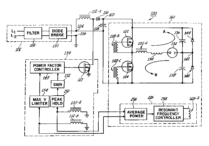
Turning now to Figure 1, a schematic block diagram of the
preferred embodiment of the circuit of the present invention is shown.
Circult 100 preferably comprises power conditioning circuit 102 to provide
a full wave rectified ac voltage between nodes 104 and 106. The power
conditioning circuit preferably includes filter 108 and diode bridge 110.
The filter is preferably an electromagnetic interference filter, to filter
noise out from lines L1 and L2. Although the line voltage at L1 and L2 is
preferably about 120 vac at 60 Hertz, the circuit of the present invention
can accommodate any line voltage and frequency. Diode bridge 110
converts the filtered line voltage from filter 108 into a full wave rectified acvoltage between nodes 104 and 106.
Transformer 112, preferably a voltage transformer, includes leg
112A, which functions as an inductor, and leg 112B, which functions as
a tap. Leg 112A stores energy therein when connected to ground via
voltage control circuit 114, and releases the stored energy when the
ground path is disconnected. When released, the stored energy in leg
112A surges through diode 116 and across capacXor 118. In the
preferred embodiment, leg 112A has an inductance value of about 172
microhenries ~LH) and capacitor 118 is about 470 microfarads (uF).
The voltage at node 120 is variable, both above and below the
value of the voltage at node 104, and is controlled by voltage control
circuit 114, via the switching frequency of FET 121, the operation of which
is explained in more detail below. As will be appreciated by those skilled
in the art, given the control over of the voltage value at node 120 relative
to that at node 104, voltage control circuit 114, in combination with leg
112A and capacitor 118, can be described as a buck-boost converter or
as a buck-boost voltage control circuit.
Ballast 160 controls the peak curren! through the lamp based on
2las~ls
LD0010265
- 7 -
the voltage at node 120. The operation of ballast 160, described generally
hereinbelow, is described in detaii in previously cross-referenced US
patent applications serial number (to be assigned) entitled "Circuit and
Method For Operating High Pressure Sodium Vapor Lamps" (attorney
5 docket LD 10,203), and US patent application serial number (to be
assigned) entitled "Feedback-Controlled Circuit and Method For Powering
A High Intensity Discharge Lamp" (attorney docket LD 10,346).
The operation of FET 122 and FET 124 are controlled by power
control circuit 126 via controlling the polarity of current through
transformer leg 128A. When transformer leg 128A is forward-biased,
transformer leg 128B is forward-biased, current flows therethrough and
FET 122 turns on. When transformer leg 128A is forward-biased,
transformer leg 128C is reverse-biased, no currentflowstherethrough and
FET 124 is off. Conversely, when transformer leg 128A is reverse-biased,
transformer leg 128C is forward-biased, current flows therethrough and
FET 124 turns on. When transformer leg 128A is reverse-biased,
transformer leg 128B is reverse-biased, no current flows therethrough and
FET 122 is off.
As FETs 122 and 124 are switched, the voltage at node 120 is
applied across the series combination of transformer leg 130A, lamp 132
and a resonant tank circuit comprising resonant inductor 134 and
resonant capacitors 136 and 138. In the preferred embodiment, resonant
inductor is about 500~ H and capacitors 136 and 138 are about 2~uF each
With reference to Figures 2 through 4, when FET 122 turns on, the
voltage at node 140 jumps to the voltage at node 120 (reference point A,
Figure 2) and the voltage at node 142 is zero (reference point A, Figure
4). Thus, current Hows in direction A through leg 130A, inductor 134,
Iamp 132, capacitor 136 and FET 122. The current flow through the lamp
increases in a resonant fashion as inductor 134 begins charging (interval
210 3 418 LD0010265 ~ ~
- 8 - ~.
A-B, Figure 3), while the voltage at node 142 increases in a resonant ~ -
fashion as capacitor 138 begins charging (interval A-B, Figure 4).
By definition, the voltage at node 142 wants to increase to twice the
voltage at node 120. However, when the voltage across capacitor 138
reaches the value of the voltage at node 120, diode 144 clamps capacitor
136 and diode 144 begins to conduct the current.
Additionally, the energy stored in inductor 134 is released as
current, discharging in a resonant fashion in direction A through lamp 132,
diode 144, FET 122 and leg 130A until the energy therein is fully
discharged (interval B-C, Figure 3). As will be appreciated by those
skilled in the art, the rate of exponential decay is based on the inductance
value of inductor 134 and the impedance value of lamp 132.
In the preferred embodiment, transformer 130 is a current
transformer and the current through leg 130A, indicative of the current
through lamp 132, is sensed by leg 130B. At some point after inductor
134 is fully discharged and the current through lamp 132 is zero, power
control circuit 126 reverses the polarity of the current through leg 128A,
turning FET 124 on and FET 122 off.
When FET 124 turns on, the voltage at node 140 is zero (reference
point C, Figure 2), while the voltage at node 142 is at the voltage value of
node 120 (reference point C, Figure 4), based on the charge stored in
capacitor 138. The voitage di~ference between node 142 and node 140
causes current to flow in direction B through lamp 132, inductor 134, leg
130A and FET 124. The current flow through the lamp increases in a
resonant fashion as inductor 134 begins charging (interval C-D, Figure 3).
As current flows, the charge stored in capacitor 138 begins to decrease
.exponentially, until the voltage at node 142 is zero (interval C-D, Figure 4).
When the voltage at node 142 is zero (reference point D, Figure 4),
diode 146 clamps capacitor 138, and the energy stored in inductor 134
, . .. . . ... . .
21~ ~ 418 LD0010265 ~ ~
g
is released as current in direction B, discharging in an exponential fashion
through leg 130A, FET 124, diode 146 and lamp 132 until fully discharged
(interval ~-A, Figure 3).
At some point after inductor 134 is fully discharged and the current
through lamp 132 is zero, power control circuit 126 reverses the polarity
of the current through leg 128A, turning FET 122 on and FET 124 off,
thereby repeating the process.
As will be appreciated by those skilled in the art, the impedance of
lamp 132 varies over time, both due to internal temperature effects, as
well as due to the deterioration of the lamp over its service life.
Additionally, variations in lamp impedance exists from one lamp to another
due to manufacturing tolerances, whether from the same manufacturer or
from one manufacturer to another. Thus, the intemal impedance of a
lamp will vsry over time, and the intemal impedance of any replacement
lamp will also vary, relative to the internal impedance of the initial lamp.
A predetermined peak current is desired to drive lamp 132 for
optimal color temperature. In order for peak current to remain constant,
any variation in lamp impedance must be met with a corresponding
variation in voltage across the lamp. Voltage control circuit 114 varies the
amount of voltage across the lamp so as to maintain a predetermined
peak current through the lamp. By varying the amount of voltage at node
120, voltage control circult 114 controls the amount of voltage seen
across lamp 132 and thus the peak current therethrough.
Voltage control circuit 114 preferably includes power factor
controller 148 which operates FET 121 based on the peak amount of
current through lamp 132. By switching FET 121 on and off, bursts of
inductance are thrown onto the line across capacitor 118, thereby
bringing the power factor substantially close to unity, e.g., 0.99.
The amount of current through leg 130A, indicative of the current
s
.. . . . .
21 ~ 3 L~ 18 LD0010265
- 10-
through lamp 132, is sensed by leg 130B, and the peak value thereof is
detected and held by peak hold circuit 150. Controller 148 compares the
peak current from peak hold circuit 150 to its internal reference and
adjusts the duty cycle of Hs output signal based on the dmerence thereof.
5 The output signal from controller 148 controls the switching frequency of
FET 121.
Controller 148 is preferably a buck-boost power factor controller,
e.g., model ML4813 available from Micro Linear Devices. The preferred
controller 148 includes therein an internal gain circuit, shown as gain
10 circuit 152. The gain circuit is set based on the system parameters, e.g.,
desired peak current through the lamp. In the preferred embodiment,
gain circuit 152 is set at about 2.5 for a peak lamp current of about 12
amps.
Transformer leg 112B functions as a voltage sensor which senses
15 the amount of energy stored in transformer leg 112A and thus provides
a scaled representation of the voltage at node 120. In order to provide
a safety feedback to controller 148, maximum voltage limiter 154 is placed
between leg 112B and controller 148. The value of the voltage at node
120 can increase above a predetermined point during the first several
20 cycles of circuit operation before the circuit reaches steady-state.
Additionally, if the lamp 132 malfunctions or is not connected, voltage at
node 120 can increase above the predetermined point because controller
148 will try to increase the voltage value at node 120 to obtain a desired
peak current. In the event the voltage increases beyond the
25 predetermined point, maximum voltage limiter 154 limits the amount of
voltage seen by controller 148. Controller 148, upon detecting a
maximum voltage condition, will output a control signal to FET 121 having
a predetermined duty cycle, switching FET 121 to provide a
predetermined voltage at node 120. In the preferred embodiment,
. . ,-
.
2 1 0 ~ 4 1 8 LDoolo265
-11 -
maximum voltage limiter 154 is set to about 300 volts.
As will be appreciated by those skilled in the art, a predetermined
amount of power is desired through lamp 132 for optimai luminance
output. With reference to Figure 3, a dead time exists from the point at
5which lamp current from the discharging inductor 134 goes to zero when
FETs 122 and 124 are switched. By varying the switching frequency of
FETs 122 and 124, the amount of dead time over a given time interval can
be controlled. Thus, by varying the switching frequency of FETs 122 and
124, power control circuit 126 controls the average power through the
10lamp. Power control circuit 126 preferably comprises average power
circuit 156, resonant frequency controller 158 and transformer leg 128A.
Average power circuit 156 preferably determines the average power
through the lamp based on the amount of current through the lamp, via
leg 130B, and the amount of voltage at node 120, via leg 112B, outputting
15a power signal indicative thereof. Resonant frequency controller 158
compares the power signal to an intemal reference value and adjusts the
rate at which the polarity of the current through leg 128A is switched
based on the dfflerence thereof. In the preferred embodiment, resonant
frequency controller 158 is a high performance resonant mode controller,
20e.g., model MC33066 available from Motorola. Additionally, transformer
128 is a voltage transformer, all three legs having an identical number of
windings, e.g., 60, about a common core.
As appreciated by those skilled in the art, color temperature of a
high-pressure sodium lamp is a function of the peak current through the
25lamp. The color temperature determines the hue of the light produced by
the lamp, commonly referred to as lamp color. It is considered important
in the art to maintain a desired color temperature so that the lamp will
have a desired lamp color. One advantage of the circuit of the present
invention is that the circuit will provide a predetermined peak current to
... ~:
2108~18 LD0010265
- 12-
the lamp, and thus a desired lamp color, despite any variations in internal
impedance over time, whether due to internal temperature effects or due
to the deterioration of the lamp over its service life. Another advantage is
that the circuit will provide a predetermined peak current to the lamp,
5 despite any dfflerence in the internal impedance from one lamp to another
due to manufacturing tolerances, whether from the same manufacturer or
from one manufacturer to another. Yet another advantage is that the
circuit will provide a predetermined peak current to the lamp despite
severe dips and/or spikes in the ac line voltage, and is in fact operable
10 regardless of the value of the ac line voltage. A further advantage is that
the power factor of the circuit is substantially close to unity, in spite of thenumerous inductors and capacitors employed therein.
Although illustrative embodiments of the present invention have
been described in detail with reference to the accompanying drawings, it
15 is to be understood that the invention is not limited to those precise
embodiments. Various changes or modifications may be effected therein
by one skilled in the art without departing from the scope or spirit of the
invention.
:, :.
. ~
. .
- -,
-
. .. :: .... : .
.. ~ . .. ..