Note: Descriptions are shown in the official language in which they were submitted.
DESCRIPTION
TITLE OF THE INVENTION
INFORMATION RECORDING MEDIUM, INFORMATION RECORDING
APPARATUS, INFORMATION REPRODUCING APPARATUS AND
INFORMATION RECORDING AND REPRODUCING APPARATUS
TECHNICAL FIELD
The present invention relate to an information
recording medium, an information recording apparatus, an
information reproducing apparatus, and an information
recording and reproducing apparatus, for example.
BACKGROUND ART
In conventional optical disks, a servo byte is
cyclically provided at a predetermined position of each track
and a clock pit for generating a reference clock and a wobble
for tracking are formed in each servo byte interval. A
reference clock (channel clock) is generated in response to
the clock pit, and information is digitally recorded by a pit
whose length is as integral multiple as the period of the
reference clock.
In a compact disc, for example, although there
exists no clock pit, information is also digitally recorded by
a pit whose length (0.9 ~m to 3.3 ~m) is as integral multiple
as the period of the reference clock (channel clock).
As described above, in the conventional optical disk
and compact disc, the pit having the length integral multiple
times as long as the period of the reference clock (channel
clock) is formed and information is recorded in response to
the length of the pit. There is then the problem that a
~j ) 'L;
recording density cannot be increased without difficulty.
When a 0.9 ~m-long pit is recorded immediately after
a 3.3 ~m-long pit was recorded, then a disc (mater recording
disc) is heated due to a so-called heat storage effect during
the 3.3 ~m-long pit is recorded so that the 0.9 ~m-long pit is
formed larger than expected. As a result, a signal is
distorted and a read-out margin of the digital signal is
reduced.
DISCLOSURE OF INVENTION
In view of the aforesaid situation, the present
invention is to increase a recording density more.
An information recording apparatus of the present
invention is significantly characterized in that information
is recorded such that a position of a leading or trailing edge
of an information pit is shifted in a step-wise fashion from a
leading or trailing edge of, for example, a reference clock or
a reference position represented by a leading or trailing edge
of a position reference pit or the like in response to digital
recording information.
An information recording medium of the present
invention is basically characterized in that the information
recording medium includes an information pit in which an edge
position is changed in response to information.
An information recording medium of the present
invention is characterized in that a phase of an information
pit is shifted by 90 degrees in adjacent tracks.
An information reproducing apparatus of the present
invention is characterized in that information is reproduced
21', '~ `;7
by detecting a shift amount of the leading or trailing edge of
the information pit from the reference position.
An information recording apparatus of the present
invention is characterized in that there is recorded a
position reference pit which expressed the reference position
of the edge of the information pit.
An information recording medium of the present
invention is characterized in that the position reference pit
indicative of the reference position of the edge of the
information pit is provided in the information pit with a
predetermined ratio.
An information reproducing apparatus of the present
invention is characterized in that the detection position of
the edge of the information pit is corrected at the detection
position of the edge of the position reference pit by a
correcting means.
An information recording medium of the present
invention is characterized in that the tracking wobble pit is
located so as to be made common in adjacent tracks.
An information recording and reproducing apparatus
of the present invention is characterized in that a polarity
of the tracking by the wobble pit is switched in the odd-
numbered track and the even-numbered track.
An information recording apparatus of the present
invention is characterized in that an information pit is
recorded such that a phase is shifted by 90 degrees in
adjacent tracks.
In an information reproducing apparatus of the
,' i `'3 ~
present invention in which the position of a front or rear
edge of an information pit is shifted in a step-wise fashion
from a predetermined reference position to thereby reproduce
recorded information from an information recording medium in
which digital information is recorded, the information
reproducing apparatus is characterized in that a clock
synchronized in phase with the reference position is
generated, the level of a reproduced signal from the
information recording medium is detected during the edge is
shifted and the position of the edge of the information is
judged from the detected level.
In an information reproducing apparatus of the
present invention in which the position of the front or rear
edge of the information pit is shifted in a step-wise fashion
from a predetermined reference position to thereby reproduce
recorded information from the information recording medium in
which digital information is recorded, the information
reproducing apparatus of the present invention is
characterized in that the position of the edge is judged on
the basis of an information point determined by the level of a
signal reproduced from the information recording medium
provided when one edge and the other edge of the adjacent
edges are located at predetermined positions.
A reference point for judging such information point
is mapped on a memory, and this information point can be
judged as a point corresponding to a reference point closest
to the mapped reference points.
Further, this mapping can be carried out by
~ ~ 3
reproducing an education pit in the information recording
medium.
of the reference points on the memory, a
predetermined reference point can be interpolated by the
calculation from the reference point determined by the
education pit.
With respect to the education pit used for the
mapping, a predetermined one can be selected from a plurality
of education pits reproduced from the information recording
medium.
The education point can be stored in a storage point
determined by an address corresponding to the reproducing
level of the education pit.
In storage points other than the storage point
determined by the address corresponding to the reproducing
level of the education pit on the memory, there can be stored
a reference point in a closest storage point of the storage
points determined by the address corresponding to the
reproducing level of the education pit.
Further, the memory can be formed of a RAM.
From the signal reproduced from the information
recording medium can be subtracted a signal corresponding to a
reference pit that is located at a shift position where a
shift amounts of two edges is smallest.
Furthermore, from the signal reproduced from the
information recording medium can be subtracted signals
corresponding to reference pits located at shift positions in
which the shift amount of two edges is smallest and the shift
amount of two edges is largest.
In an information recording medium in which a
position of a front or rear edge of an information pit is
shifted in a step-wise fashion from a predetermined reference
position to thereby record digital information, the
information recording medium of the present invention is
characterized in that there is formed an education pit having
education data used to generate a reference point that is used
to judge an information point determined by the level of a
signal reproduced from an information recording medium
provided when one edge and the other edge of the adjacent
edges are located at predetermined positions.
The education data at the education pit can be
formed on the opposite side of data pit.
A reference pit having two edges located at a shift
position in which the shift amount is smallest can be recorded
at a predetermined position other than the data pit.
A reference pit having two edges located at a shift
position in which the shift amount is largest can be recorded
at a predetermined position other than the data pit.
Furthermore, reference pits having two edges located
at the shift position where the shift amount is smallest and
two edges located at the shift position where the shift amount
is largest can be recorded at predetermined positions other
than the data pit.
BRIEF DESCRIPTION OF DRAWINGS
FIG. 1 is a diagram used to explain a principle by
which information is recorded according to an edge of an
r. i 3
information pit of the present invention, FIG. 2 is a diagram
used to explain an information recording format of one sector
according to the present invention, FIG. 3 is a diagram used
to explain a principle of how to read out data from a position
of an edge of an information pit according to the present
invention, FIG. 4 is a diagram used to explain an influence of
a fluctuation of sensitivity of an optical disk, FIG. 5 is a
diagram used to explain action of a position reference pit of
the present invention, FIG. 6 is a diagram used to explain the
state of output obtained when a correction using the position
reference pit of the present invention is not carried out,
FIG. 7 is a diaqram used to explain the state of output
obtained when a correction using the position reference pit of
the present invention is carried out, FIG. 8 is a diagram used
to explain the state that a phase of the information pit is
shifted by 90 degrees in adjacent tracks according to the
present invention, FIG. 9 is a diagram used to explain the
tracking state based on the 3-spot system, FIG. 10 is a
diagram used to explain the tracking state based on the 3-spot
system effected when a track pitch is reduced, FIG. ll is a
diagram used to explain the tracking state based on a wobbled
pit, FIG. 12 is a diagram used to explain the tracking state
based on the wobbled pit effected when the track pitch is
reduced, FIG. 13 is a diagram used to explain an arrangement
of pits near a servo area of the optical disk according to the
present invention, FIG. 14 is a diagram used to explain a
difference between the information pit of the present
invention and a pit of other information recording medium,
/S~
FIG. 15 is a block diagram showing an arrangement of a part of
an embodiment of an information recording apparatus according
to the present invention, FIG. 16 is a block diagram showing
an arrangement of other portion of the embodiment of the
information recording apparatus according to the present
invention, FIG. 17 is a timing chart used to explain operation
of the embodiment of FIG. 16, FIG. 18 is a block diagram
showing an arrangement of an embodiment of an information
reproducing apparatus according to the present invention, FIG.
l9 is a block diagram showing an arrangement of an embodiment
of a tracking servo apparatus in an information recording and
reproducing apparatus of the present invention, FIG. 20 is a
diagram used to explain a track format of an information
recording medium of the present invention, FIG. 21 is a
diagram used to explain an example of an arrangement of an
information pit in the information recording medium of the
present invention, FIG. 22 is a block diagram showing an
arrangement of an embodiment of an optical disk reproducing
apparatus to which the information reproducing apparatus of
the present invention is applied, FIG. 23 is a block diagram
showing an example of an arrangement of a two-dimension
decoder in the embodiment of FIG. 22, FIG. 24 is a block
diagram showing an example of arrangements of a bias
eliminating circuit and the two-dimension decoder in the
embodiment of FIG. 22, FIG. 25 is a diagram used to explain an
intersymbol interference in the adjacent edges, FIG. 26 is a
diagram used to explain a principle of a mapping of a
reference point in a RAM, FIG. 27 is a diagram used to explain
~.
a function that shows an influence of adjacent edges, FIG. 28
is a diagram used to explain a relationship between the
influence of adjacent edges and a linear density, FIG. 29 is a
timing chart used to explain operation of a servo area in the
embodiment of FIG. 24, FIG. 30 is a diagram used to explain
the mapping of reference points on the RAM of FIG. 24, FIG. 31
is a diagram used to explain the mapping of reference points
corresponding to other storage points in the RAM of FIG. 24,
FIG. 32 is a diagram used to explain a mapping information of
reference points corresponding to all storage points on the
RAM of FIG. 24, FIG. 33 is a timing chart used to explain
operation in a data area of the embodiment of FIG. 24, FIG. 34
is a diagram used to explain an example of other arrangement
of the information recording pit, FIG. 35 is a diagram showing
an example of an arrangement of a servo area provided when an
information recording pit is arranged as shown in FIG. 34,
FIG. 36 is a diagram used to explain an error rate that is
realized by the embodiment of FIG. 24, FIG. 37 is a block
diagram showing an arrangement of other embodiment of the
optical disk reproducing apparatus to which the information
reproducing apparatus of the present invention is applied,
FIG. 38 is a timing chart used to explain operation of the
embodiment of FIG. 37, FIG. 39 is a diagram used to explain
the change of the level of an output from a gain variable
amplifier in FIG. 37, FIG. 40 is a diagram used to explain an
error occurrence situation that is realized in the embodiment
of FIG. 37, FIG. 41 is a block diagram showing an arrangement
of a further embodiment of the optical disk reproducing
) L'~
apparatus to which the information reproducing apparatus of
the present invention is applied, FIG. 42 is a diagram used to
explain operation of a defect eliminating circuit of FIG. 41,
FIG. 43 is a block diagram showing an example of an
arrangement of the defect eliminating circuit of FIG. 41, FIG.
44 is a diagram of a table used to explain a calculation in a
controller in FIG. 43, FIG. 45 is a diagram used to explain an
influence of a defect of the output of the gain variable
amplifier in FIG. 41, and FIG. 46 is a block diagram showing
an example of other arrangement for calculating a minimum
distance between education data and reproduced data.
BEST MODE FOR CARRYING OUT THE INVENTION
Embodiments of the present invention will be
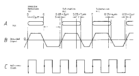
described hereinafter. FIG. 1 shows a recording principle of
the present invention. As illustrated, according to the
present invention, the position of at least one of the leading
and trailing edges of an information pit (both the leading and
i trailing edges in this embodiment) is shifted in a step-wise
fashion from the position of the reference edge in response to
a digital recording informa~ion.
More specifically, the position (zero-cross
. .,
position) of the edge of a recorded signal shown in FIG. lB is
delayed or advanced in a step-wise fashion by a predetermined
time with reference to the position of the leading edge of the
reference clock shown in FIG. lC in response to recorded
information. In this embodiment, the edge position is delayed
so that the edge position is moved rightward from the
reference position in the figure. When the above-mentioned
,~ .1 ',~ ,' ~' '
ll
edge position is advanced from a time standpoint, the edge
position is moved leftward in the figure.
Assuming that each edge represents 3-bit digital
data (i.e., [O], [7]), then each edge is formed at the
reference position when data is [O], each edge is delayed by a
unit delay time (one step) when data is [O], each edge is
delayed twice (2 steps) of the unit time when data is [1], and
each edge is delayed by three times (3 steps) of the unit time
when data is [3]. In a like manner, when data is [7], the
edge is delayed seven times (7 steps) of the unit time.
When information is recorded as described above,
information pits are formed on the optical disk as shown in
FIG. lA. The information pit can be formed as a physical
concave or convex portion and also can be formed by making the
characteristics (e.g., reflectivity or transmittance, etc.) of
the information recording medium different from those of other
portion. In this embodiment, [3] and [7] are expressed by the
leading edge and the trailing edge of the first information
pit following the position reference pit (position reference
pit will be described later on), and [O] and [4] are expressed
by the leading edge and the trailing edge of the next
information pit. Assuming that 0.05 ~m is a length on the
recording medium corresponding to the unit time (one step) of
the delay of the recorded signal, then the respective edges
are shifted rightward by 3 x 0.05 ~m, 7 x O.OS ~m, O x O.OS ~m
and 4 x O.OS ~m from the reference position. A length (length
provided when neither of the leading and trailing edges are
delayed) on the optical disk correspondin~ to one period of
.
12
the reference clock is set to be 1.2 ~m.
When the edge of the information pit is shifted from
the reference position in response to the digital recording
information as described above, the reference position of the
edge must be clarified. To this end, as shown in FIG. 2, a
PLL clock (clock pit) is recorded in the information recording
medium at a constant period (e.g., one rotation of the optical
disk is segmented into 4200 sectors and one servo area is
provided in each sector so that such pit is recorded with a
ratio of one pit to each servo area).
When information is recorded, this PLL pit (clock
pit) is reproduced and the reference clock (FIG. lC) is
generated in synchronism with this pit. The reference
position of the edge is determined on the basis of this
reference clock (the leading edge of the reference clock is
used as the reference position of the edge of the information
pit in this embodiment). There are formed a plurality of
information pits between this clock pit and the clock pit.
FIG. 3 shows a principle in the reproducing mode.
Upon playback, an RF signal shown in FIG. 3A is obtained by
reproducing an optical disc in which information is recorded
as shown in FIGS. 1 and 2. If this RF signal is amplified and
converted into a binary signal, then there is obtained a
binary RF signal shown in FIG. 3B. When the clock pit (PLL
pit) is separated from this binary RF signal and synchronized,
then there is generated a reference clock shown in FIG. 3C.
Further, a sawtooth wave signal (might be a triangular wave
signal) shown in FIG. 3D is generated in synchronism with this
' 1 3 1
13
reference clock.
This sawtooth wave signal reaches a maximum level
[255] immediately before the trailing edge of the reference
clock, is suddenly lowered to the minimum level after the
trailing edge and is then increased again to the maximum value
linearly. Therefore, the level of 256 steps can be judged by
this sawtooth wave signal. Accordingly, the level (shift of
the edge of the information pit) of the sawtooth wave signal
(FIG. 3D) in the timing of the leading edge and the trailing
edge of the binary RF signal (FIG. 3B) is detected. Also, the
level (reference position of the edge of the information pit)
of the sawtooth wave signal (FIG. 3D) in the leading edge of
the reference clock (FIG. 3C) is detected. Then, the shift
(i.e., recorded data) from the reference position of the edge
of the information pit can be detected on the basis of the
difference therebetween.
If a sensitivity of the optical disc is fluctuated
or a recording laser power is fluctuated from a time
standpoint, then pits to be formed also are fluctuated. FIG.
4 shows this state. More specifically, when a recording laser
light of the same level (intensity) is radiated, if a
sensitivity of the optical disk is low, then the length of a
pit to be formed is reduced as compared with that of the case
where a sensitivity is high. Also, even when the sensitivity
is constant, if a power of a recording laser light is
fluctuated, then a similar fluctuation occurs.
If such fluctuation occurs, then it becomes
impossible to form, i.e., record accurate information at the
1 4
accurate position of the above-mentioned edge. Therefore, in
this embodiment, the position reference pit is recorded at a
constant period in addition to the reference pit (PLL pit).
In this embodiment, one position reference pit is formed
immediately after the clock pit (i.e., one position reference
pit is formed in each sector) and a plurality of information
pits are formed after the clock pit. Both the leading edqe
and the trailing edge of the position reference pit are
constantly located at the reference position (at the position
of the leading edge of the reference clock).
Action of the position reference pit will be
described with reference to FIG. 5. As shown in FIG. 5A, the
initial pit is selected to be the position reference pit and
therefore data corresponding to both edges are set to [o]~
With the leading edges and trailing edges of three information
pits following the position reference pit are associated data
of [3] and [O], [2] and [5], and [1] and [O], respectively.
Therefore, assuming now that the optical disc has a proper
sensitivity, then there are formed position reference pits and
information pits shown in FIG. 5C on the optical disk in
response to a recording signal (recording pulse) shown in FIG.
5B.
Upon playback, when the leading and trailing edges
of each pit are detected and the level of a sawtooth wave
signal shown in FIG. 5D in that detection timinq is read out,
values in the leading and trailing edges of the position
reference pit are both ~64). In that case, when the leading
and trailing edges of three information pits are detected and
~ ,. 3 ~ ;
the levels of the sawtooth wave signals in that detection
timing are detected, the detected levels are [82] and [64],
[76] and [94], and [70] and [64] as shown in EIG. 5E,
respectively. In order to calculate shifted amount of these
values from the reference position, the levels of the sawtooth
wave signals in the leading edges of the reference clocks in
the respective pits are detected and the detected values are
subtracted as described above. The level of the sawtooth wave
signal in the timing of the edge of the reference clock
becomes the same as the level of the position reference pit.
Accordingly, instead of reading out the level of the sawtooth
wave signal corresponding to the edge of the reference clock
at every pit, the levels of the sawtooth wave signals in the
leading and trailing edges of the position reference pit and
the level of the sawtooth wave signal corresponding to the
edge of the reference clock at every pit can be used as the
level of the sawtooth wave signal corresponding to the edge of
the reference clock at every pit (second effect of the
position reference pit can be achieved in addition to a
sensitivity correcting action (first effect) which will be
described later on).
In the case of this embodiment, by subtracting the
values [64] and [64] in the position reference pit from the
values shown in FIG. 5E, i.e., [82] and [64], [76] and [94]
and [70~ and [64], ~18] and [O], [12] and [30], [6] and [O]
can be obtained as values corresponding to the shifted amount
as shown in FIG. 5F, respectively. Of these shifted amount,
the value [6] corresponds to the above-mentioned unit delay
~ 1 3 ~ L . i D
16
time so that [3] and [o]l [2] and [5] and [1] and [o] can be
obtained by dividing these values by [6], respectively. These
values become the same as the original data shown in FIG. 5A.
When a sensitivity of the optical disk is too high,
as shown in FIG. 5G, the position reference pit and the
information pit are extended in response to the recording
pulse shown in FIG. 5B as compared with the case of the proper
sensitivity shown in FIG. 5C. The fluctuation of sensitivity
becomes substantially constant in one optical disk regardless
of a fluctuation of each optical disk. Even if a local
fluctuation occurs in one optical disk, then it is to be
considered that such fluctuation of sensitivity is
substantially constant in a range (within one sector) of a
period in which at least the position reference pit is formed.
Therefore, assuming that the position of the leading
edge in the position reference pit is reduced by [10] from the
conventional reference position in the terms of the level of
the sawtooth wave signal (FIG. 5H) as shown in FIG. 5I, then
the position of the trailing edge is increased by [10~ from
the original reference position in terms of the level of the
sawtooth wave signal. Consequently, they become [54] (= 64 -
10) and [74] (= 64 + 10). Similarly, the positions of the
leading edge and the trailing edge of each information pit are
reduced or increased by [10) from the original recording
position in terms of the level of the sawtooth wave signal.
More specifically, values of the sawtooth wave signal (FIG.
5H) in the timings of the leading edge and the trailing edge
of respective information pits (FIG. 5G) become [72] (= 82 -
r~
1710) and [74] (= 64 + 10), [66~ (= 76 - 10) and [104] ~= 94 +
100, [60] (= 70 - 10) and [74] (= 64 + 10) as shown in FIG.
5I, respectively.
Accordingly, by subtracting the reference pit values
[54] and [74] from these information pit values [72] and [74],
[66] and [104] and [60] and [74], [18] and [0], [12] and [30],
and [6] and [0] are obtained as shown in FIG. 5J,
respectively. These values become the same as those of the
proper sensitivity shown in FIG. 5F (this is the first effect
achieved by the position reference pit).
While the present invention has been described so
far in association with the case that the sensitivity is too
high, when the sensitivity is too low, the edge of the
information pit is reduced by the same length as that of the
edge of the position reference pit so that, similarly to the
case that the sensitivity is too high, the same data as those
in the case of the proper sensitivity can be obtained.
More specifically, since the position reference pit
is formed as described above, the sawtooth wave signal need
not be read at every reference clock of each pit. Also, even
when a fluctuation of sensitivity or the like occurs, the
recording and reproduction of correct data become possible.
FIGS. 6 and 7 are diagrams used to explain the
effects achieved by the correction by using the position
reference pit. In both figures, the abscissa represents a
time and the ordinate represents a voltage. The voltage on
the ordinate represents data from [0] to [7] shown in FIG. 1
in terms of voltage. That is, when the shift amount (this
'J~
18
shift amount is any one of the aforementioned [o] to [7]) of
the edge obtained at a certain time (predetermined position on
the abscissa) from the reference position is [O], such edge is
expressed by a point of the lowest predetermined voltage. If
such shift amount is [7], then the edge is expressed by a
point of the highest predetermined voltage. Data that are
expressed by respective edges of successively reproduced
information pits are expressed in the form of points of the
predetermined voltages (such waveforms are obtained by
monitoring an output of a D~A converter 47 in FIG. 18 that
will be described later on).
FIG. 6 shows the state that the correction is not
carried out by using the position reference pit. In the case
of this figure, points that should be arranged on a horizontal
line indicative of a constant voltage are considerably
shifted on the ordinate direction at every data of [O] to [7].
This means that, even in the edge that expresses the same [5],
its shift aMount from the reference position is increased
(e.g., shift amount (voltage) that inherently expresses the
data [7]) or decreased (e.g.. shift amount (voltage) that
inherently expresses the data [3]) depending on the cases,
i.e., the shift amount is changed. In order to determine
(identify) that data is any one of [O] to [7], an intermediate
voltage between a voltage (shift amount) indicative of one
data (e.g., [5]) and a voltage (shift amount) indicative of
adjacent data (e.g., [6]) must be selected to be a threshold
value and it must be determined whether or not the voltage is
larger or smaller than the threshold value. However, when
19 ~3 i1 '' "
voltages that indicate respective data are fluctuated as shown
in FIG. 6, it becomes impossible to determine (identify)
whether or not data is data ([5] or [6]) that is based on the
fixed predetermined threshold voltage.
FIG. 7 shows the case that the correction by the
position reference pit is carried out. In this case, it is to
be appreciated that voltages (shift amounts) of respective
data become constant. Accordingly, in this case, respective
data can be identified with ease on the basis of a
predetermined threshold value.
FIG. 8 shows a relationship between pits (position
reference pit and information pit) in adjacent tracks. In the
case of a CAV (rotation angular velocity is constant) disc, as
shown in the figure, phases (phases provided when data is [o])
of the pits of adjacent tracks (odd-numbered track and even-
numbered track) are shifted by 90 degrees. In other words,
the phase of the recording signal provided when the data is
[0] is shifted by 90 degrees. This also means that the phase
of the reference clock of the odd-numbered track is shifted
from the phase of the reference clock of the even-numbered
track by 180 degrees when the phase of the reference clock is
considered. With the above-mentioned arrangement, when the
edge of one position reference pit or information pit of one
track is reproduced by one beam spot, the edges of the
adjacent tracks do not locate in the beam spot so that a
crosstalk is reduced. Accordingly, the track pitch is reduced
and a higher density recording can be realized.
The tracking method will be described next. As one
of the tracking methods, there is known a so-called three-spot
(beam) method. According to this method, as shown in FIG. 9,
two sub beams (spots) are provided at both sides of a main
beam (spot) that is inherently provided to reproduce
information. By arranging the sub beams at the right and left
edges of the track direction, it is possible to detect
reflected beams from the two sub beams by a photo-detector.
Accordingly, a tracking error signal can be obtained from a
difference between the outputs. However, according to this
method, as shown in FIG. 10, if the track pitch is reduced,
the sub beam reads out information from the adjacent track and
a tracking error signal cannot be generated.
Some optical disks employ a so-called sample servo
system. According to this method, as shown in FIG. 11,
wobbled pits are located at the positions slightly displaced
from the center of the track in the right and left direction
and which are also displaced in the track direction. A
tracking error signal can be generated from a level difference
of the reproduced signals of the two wobbled pits. However,
also in this method, if the track pitch is reduced, then as
shown in FIG. 12, the wobbled pits for the adjacent tracks
interfere with each other so that a correct tracking error
signal cannot be generated.
Therefore, this embodiment adopts the sample servo
system shown in FIG. 11 fundamentally. As shown in FIG. 13,
on the servo area, there are provided one clock pit (PLL pit)
that is located on the central line of the track and two
wobbled pits which are displaced from the central line of the
21
track in the right and left direction and which are also
displaced in the track direction (so as to oppose to each
other across the clock pit). These pits are recorded (formed)
in advance as, for example, physical concave and convex
portions before original information is recorded. Then, the
respective wobbled pits are arranged so that they can be used
commonly on the adjacent tracks. In other words, the wobbled
pit is just located between the tracks. One wobbled pit is
used for the right and left tracking. With this arrangement,
the track pitch can be reduced and the tracking error signal
can be generated.
When one wobbled pit is used both in the right and
left tracks, a polarity of the tracking servo must be inverted
at odd-numbered track and even-numbered track. An embodiment
of this case will be described later with reference to FIG.
19 .
When the phase of the position reference pit and the
phase of the information pit are displaced 90 degrees on the
odd-numbered track and even-numbered track, as shown in FIG.
13, the position of the last information pit in one (even-
numbered track in this embodiment) of, for example, the even-
numbered track or odd-numbered track is displaced in the
rearward from the other track (even-numbered track in this
embodiment). Observing such phenomenon on a time axis (on a
reproduced signal), the last information pit appears in the
even-numbered track with a delay as compared with the case of
the odd-number-ed track. Alternatively, examining the position
reference pit located immediately after the clock pit, the
~ J_ J ~
22
position reference pit appears in the even-numbered track with
a delay as compared with the case in the odd-numbered track.
Accordingly, the odd-numbered track or even-numbered track can
be judged by detecting the timing at which the last
information pit or position reference pit is generated. This
embodiment also will be described later with reference to FIG.
19 .
In order 'o more clarify the specific features of
the information recording method according to the present
invention, the conventional recording method and the recording
method of the present invention are compared with reference to
FIG. 14. In the optical disk of the conventional sample servo
system, as shown in FIG. 14A, a reference clock (channel
clock) is generated in synchronism with the clock pit. Then,
the period of reference clock is taken as one unit and a pit
having a lenqth of an integral multiple of such unit is
formed. The length of the pit depends on recording
information.
Further, although the clock pit is not formed in the
compact disc, as shown in FIG. 14B, the period of the
reference clock (channel clock) is taken as one unit and a pit
having a length of an integral multiple thereof is formed.
On the other hand, according to the embodiment of
the present invention, as shown in FIG. 14C, the reference
clock is generated in synchronism with the clock pit (PLL pit)
similarly to the case of FIG. 14A. However, the length of the
information pit is basically selected to be the length of the
period of the reference clock (position of the edge in this
23
case is selected to be the reference position), and that
length is changed in accordance with the recorded data. What
is important as information is the shift amount of the edge
from the reference position. Therefore, according to this
embodiment, the length of the information pit is set to be
more than one time and less than twice the period of the
reference clock.
As is clear from the comparison of FIG. 14C with
FIGS. 14A, 14B, according to this embodiment, the information
recording of higher density becomes possible. Then, in order
to determine the reference position more accurately, the
position reference pit is inserted in addition to the clock
pit, if necessary.
In the case of the compact disc, the track pitch is
1.6 ~m, and the recording density is 0.6 ~m per bit. On the
other hand, according to this embodiment, the track pitch
could be selected to be 1.2 ~m, and the recording density
could be selected to be 0.4 ~m per bit. Therefore, there can
be realized the recording density that is twice as high as
that of the compact disc.
An embodiment of an apparatus that can realize the
above-mentioned recording and reproducing will be described
next. FIG. 15 shows an arrangement of a part of a recording
apparatus. A data output circuit 15 A/D converts a signal
supplied thereto from a circuit, not shown, processes the same
in a predetermined fashion and outputs the signal thus
processed to an error correction ~ECC) circuit 52. The error
correction circuit 52 effects the processing such as the
~ J ~
24
addition of an error correction code, the interleaving or the
like on the input digital data. A data length converting
circuit 53 converts data of, for example, 8 bits input thereto
from the error correction circuit 52 into data of 3 bits. The
data of 3-beam unit is supplied to a recording apparatus shown
in FIG. 16.
A reference clock (FIG. 17A) is supplied to a
terminal 11 of FIG. 16. This reference clock is generated by
a PLL circuit 31 of FIG. 18, which will be described later on,
in synchronism with the clock pit of the optical disk. The
reference clock is supplied through a buffer 12 and a switch
14 to a delay line 15. The switch 14 is changed in position
to a contact a side on the odd-even number track and to a
contact b side on the even-numbered track, respectively. When
the switch is connected to the contact b side, the reference
clock is inverted by an inverter 13 and then input to the
delay line 15. The other end of the delay line 15 is grounded
via a resistor 16.
The delay line 15 includes 8 output terminals each
having a buffer 17 and outputs thereof have delay times which
are different at the unit time each. More specifically, this
unit time is set to a time corresponding to the length of 0.05
~m on the optical disk. That is to say, from each output
terminal, there is output a reference clock that is delayed by
a delay time of unit time x O time to unit time x 7 times. A
data selector 10 selects any one of the 8 output terminals in
response to the 3-bit data supplied thereto from the data
length converting circuit 53. More specifically, the data
selector selects an output terminal having a delay time of
unit time x 0 (i.e., outputs a reference clock that is not
delayed) when data is [o]~ and also selects an output terminal
having a delay time of unit time x S when data is [5].
Therefore, the reference clock is delayed in a step-wise
fashion in which the unit time is one step by a delay time
corresponding to the digital data. When the position
reference pit is recorded, [0] is input to the data selector
10 as data. Accordingly, the reference clock that is not
delayed is output from the data selector 10.
A T-type flip-flop 18 is triggered at the leading
edge of the output from the data selector 10. Each time the
flip-flop is triggered, the logic level of its output is
inverted. An output of this T-type flip-flop 18 is supplied
to one input of an AND gate 20.
An N-scale counter 23 counts the reference clock. A
decoder 24 counts a count value of this counter and generates
a signal of a logic level L during the servo area interval of
each sector and a signal of a logic level H (see FIG. 17~) of
a data interval of each sector. This signal is supplied to a
reset terminal of the T-type flip-flop 18 and the other input
of the AND gate 20.
Therefore, in the data interval, the AND gate 20 is
energized so that a recording pulse (FIG. 17C) whose leading
and trailing edges are delayed in a step-wise fashion by a
time corresponding to the 3-bit data output from the T-type
flip-flop 18 is output through the AND gate 20. The signal
output from the AND gate 20 is supplied to a recording head
26
not shown) for the optical disk as a recording signal and is
thereby recorded on the optical disk. During the servo area
interval, the AND gate 20 is de-energized to inhibit the
recording signal from the T-type flip-flop 18 from being
output.
A reproducing apparatus will be described with
reference to FIG. 18. A reproduced RF signal played back from
the optical disk is input to a PLL circuit 31 and an equalizer
34. The PLL circuit 31 extracts the component of the above-
mentioned clock pit (PLL pit) from the RF signal (FIG. 3A~ to
generate the reference clock (FIG. 3C) which is then supplied
to a sawtooth wave oscillator 33. The sawtooth wave
oscillator 33 generates a sawtooth wave signal (FIG. 3D) in
synchronism with the reference clock input thereto and outputs
the same to A/D converters 36, 37. Further, the reference
clock generated by the PLL circuit 31 is also supplied to a
timing controller 32, and the timing controller 32 supplies a
latch pulse at the timing of the above-mentioned position
reference pit (FIG. 3A) to a latch circuit 40 in synchronism
with the reference clock and also supplies a latch pulse at
the timing of the trailing edge to a latch circuit 42.
The equalizer 34 processes the RF signal input
thereto such that this signal has a predetermined frequency
and phase characteristic. Then, the equalizer outputs the
signal thus processed to a binary circuit 35. The binary
circuit 35 converts the input RF signal into a binary signal.
The binary RF signal (FIG. 3B) is supplied to a clock terminal
of the A/D converter 36 and a clock terminal of a latch
27
circuit 39. This signal is also inverted by an inverter 38
and then supplied to the clock terminal of the A/D converter
37 and to a clock terminal of a latch circuit 41.
Therefore, in the A/D converter 36, the level of the
sawtooth wave signal (FIG. 3D) at the timing of the leading
edge of the binary RF signal is sampled and then a sampled
value thereof is A/D-converted. Because the level of the
sawtooth wave signal is analyzed into 256 steps as described
above, this sampled value is output to the latch circuit 39
and 40 as 8-bit data. The latch circuit 39 latches the output
of the A/D converter 36 at the timing of the leading edge of
the binary RF signal output from the binary circuit 35.
Further, the latch circuit 40 latches the output of the A/D
converter 36 at the timing of the leading edge of the position
reference pit output from the timing controller 32.
As described above, data (reference position data)
[64] of the leading edge of the position reference pit
described in FIG. 5E or data (reference position data) [54] of
the leading edge of the position reference pit described in
FIG. SI is latched in the latch circuit 40. Further, data
(data displaced from the reference position) [82], [76], [70]
of the leading edge of the information pit described in FIG.
SE or data (data displaced from the reference position) [72],
[66], [60] of the leading edge of the information pit
described in FIG. 5I is latched in the latch circuit 39. A
subtracter 43 subtracts the latched data of the latch circuit
40 from the latched data of the latch circuit 39. The
subtracter 43 subtracts the latched data of the latch circuit
~ J ~ ?s
28
40 from the latched data of the latch circuit 39, thereby
producing values [18], [12], [6] indicative of the
displacement of the leading edge of information pit described
in FIG. 5F from the reference position or corrected values
[18]. [12], [6] indicative of the displacement of the leading
edge of information pit described in FIG. 5J from the
reference position.
The 8-bit data output from the subtracter 43 is
converted into 3-bit data by a conversion map circuit 45 and
then output. If the output of the subtracter 43 is D/A-
converted by a D/A converter circuit 47 and then mGnitored,
then the characteristic shown in FIG. 7 (or FIG. 6) can be
monitored as described above.
On the other hand, the level of the sawtooth wave
signal at the timing of the trailing edge of the binary RF
signal is sampled by the A/D converter 37, and its sampled
value is A/D converted thereby. This sampled value is output
to the latch circuits 41, 42 as 8-bit data. The latch circuit
41 latches the output of the A/D converter 37 at the timing of
the trailing edge of the binary RF signal. Further, the latch
circuit 42 latches the output of the A/D converter 37 at the
timing of the trailing edge of the position reference pit
output from the timing controller 32.
As described above, the data (reference position
data) [64] of the trailing edge of the position reference pit
described in FIG. 5E or data (reference position data) [74] of
the trailing edge of the position reference pit described in
FIG. 5I is latched in the latch circuit 42. Further, data
29
(data shifted fronl the reference position) [64], [94]/ [64] of
the trailing edge of the informatlon pit described in FIG. 5E
or data (data shifted from the reference position) [74],
[104]. [74] of the trailing edge of the information pit
described in FIG. 5I are latched in the latch circuit 41. The
subtracter 44 subtracts the latched data of the latch circuit
42 from the latched data of the latch circuit 41, thereby
obtaining values [0], [30], [0] indicative o the displacement
of the trailing edge of the information pit described in FIG.
5F from the reference position or corrected values indicative
of the displacement of the trailing edge of the information
pit described in FIG. 5J from the reference position.
The 8-bit data output from the subtracter 44 is
converted into 3-bit data by a conversion map circuit 46 and
then output.
While the two A/D converters are used as described
above, the present invention is not limited thereto and only
one converter may be sufficient such that the signal from the
binary circuit 35 or the inverter 3a is switched to and then
supplied to the clock terminal thereof. Further, a sample
and hold circuit may be used instead of the A/D converter.
Furthermore, even when a count clock having a frequency
sufficiently higher than the reference clock is generated at a
predetermined period in synchronism with the reference clock,
such count clock is counted by a counter and then latched at
the timing of the leading edge or trailing edge of the binary
RF signal, then the displacement of the edge can be detected.
While the data of the position reference pit at
every sector is solely latched by the latch circuits 40 and 42
and used for correction, the present invention is not limited
thereto and such a variant is also possible that an average
value of values in a plurality of sectors is obtained and can
be used for correction. If so, then a reliability can be
increased more.
FIG. 19 shows a circuit arrangement such that, as
shown in FIGS. 8 and 13, the odd-numbered track and the even-
numbered track are judged in the optical disc having the
format in which the wobbled pit is made common in the adjacent
tracks and 'he phases of the position reference pit and the
information pit are shifted by 90 degrees between the adjacent
tracks and the polarity of the tracking servo is switched in
response to the judged result. In this embodiment, a
reproduced RF signal reproduced and output from the optical
disc is supplied to a PLL circuit 61 and a sample and hold
circuit 63. The PLL circuit 61 generates a reference clock
from a component corresponding to the reference pit and
outputs the same to a timing circuit 62. The timing circuit
62 generates a variety of timing signals synchronized with the
reference clock supplied from the PLL circuit 62 and supplies
the same to sample and hold circuits 63, 66 and 67.
As earlier noted with reference to FIG. 13, if the
phase of the pit is shifted by 90 degrees, then the timing at
which the last information pit (or position reference pit)
becomes different at the odd-numbered track and the even-
numbered track. The timing circuit 62 outputs the sampling
pulse to the sample and hold circuit 63 at the timing in which
31
the last information pit exists in the even-numbered track and
in which the last information pit does not exist in the odd-
numbered track (see FIG. 13). Since the information pit
exists in the even-numbered track, the level of the RF signal
at the timing in which the sampling pulse is input is small.
On the other hand, since no information pit exists in the odd-
numbered track, the level of the RF signal is larger than that
of the case of the even-numbered track.
Accordingly, the level of the RF signal at the
timing in which the sampling pulse is input is sampled and
held in the sample and hold circuit 63 and this sampled and
held value is compared with a reference voltage output from a
reference voltage generating circuit 65 by a comparing circuit
64. This reference voltage is set to an intermediate value
between the sampled and held value in the odd-numbered track
and the sampled and held value of the even-numbered track.
Therefore, in the case of the odd-numbered track, the output
of the comparing circuit 64 goes to high level, while in the
case of the even-numbered track, that output goes to low
level. This output is used to change-over the switch shown in
FIG. 16 and is also used to change-over a switch 68 of a
tracking servo circuit 80.
The timing circuit 62 supplies the sampling pulse to
the sample and hold circuit 66 at the timing of one wobbled
pit shown in FIG. 13, and supplies the sampling pulse to the
sample and hold circuit 67 at the timing of the other wobbled
pit. Accordingly, the sample and hold circuits 66 and 67
sample and hold therein the levels of the RF signals at the
,!~lj .,
32
timings of the two wobbled pits. A differential amplifier 69
subtracts the output of the sample and hold circuit 67 from
the output of the sample and hold circuit 66 to generate a
tracking error signal. This tracking error signal is supplied
to a tracking actuator 70, thereby the tracking control being
effected. An input terminal of the differential amplifier 69
to which the outputs of the sample and hold circuits 66, 70
are supplied is switched oppositely (opposite polarity side)
by the switch 68 in the odd-numbered track and in the even-
numbered track. Therefore, even when the wobbled pit is
commonly used in the adjacent tracks, the correct tracking
servo is executed.
According to the information recording apparatus of
the above-mentioned embodiment, since the edge position of the
information pit is shifted in a step-wise fashion in response
to the recording information from the reference position to
thereby record digital information, digital information can be
recorded at higher density.
According to the information recording medium of the
above-mentioned embodiment, since the information pit is
formed such that the position of the edge is changed in a
step-wise fashion in response to the recording information, it
is possible to realize the information recording medium of
higher recording density.
According to the information recording medium of the
above-mentioned embodiment, since the phase of the information
pit is shifted by 90 degrees in the adjacent tracks, it is
possible to realize the information recording medium having a
33
narrow track pitch and having less crosstalk.
According to the information reproducing apparatus
of the above-mentioned embodiment, since the displacement of
the edge of the information pitch from the reference position
is detected, digital information that was recorded with high
density can be reproduced accurately.
According to the information recording apparatus of
the above-mentioned embodiment, since the position reference
pit indicative of the reference position of the edge of the
information pit is recorded, a velocity of the information
recording medium can be controlled with ease upon recording.
According to the information recording medium of the
above-mentioned embodiment, since the position reference pit
indicative of the edge of the information pit is disposed on
the information pits with the predetermined ratio, an
influence of jitter upon reproduction can be made small and it
is possible to realize the information recording medium from
which information can be read out accurately.
According to the information reproducing apparatus
of the above-mentioned embodiment, since the detection
position of the edge of the information pit is corrected by
the detection position of the edge of the reference pit, an
influence of jitter can be made small and it becomes possible
to read out information accurately.
According to the information recording medium of the
above-mentioned embodiment, since the wobbled pit for tracking
is arranged so as to be used commonly in the adjacent tracks,
the track pitch can be made narrower.
~ "J ~ ~
34
According to the information recording and
reproducing apparatus of the above-mentioned embodiment, since
the polarity of the tracking by the wobbled pitch is switched
on the odd-numbered track and the even-numbered track, the
phase of the information pit is shifted by 90 degrees in the
information recording apparatus of the above-mentioned
embodiment which can effect the accurate tracking even when
the track pitch is narrow, the track pitch can be made narrow
and information can be recorded.
FIG. 20 shows a fundamental format of an optical
disc to which there is applied an information recording medium
according to other embodiment of the present invention. In
this embodiment, a servo area is provided in each track at a
constant period and a data area is formed between the servo
area and the servo area. The servo area has 5 pits and the
data area has 44 pits. Of 5 pits of the servo area, two pits
are assigned to education pits P1, P2 and remaining 3 pits are
assigned to reference pits P3 through P5. The edge on the
left-hand side of the education pit P2 is set to a position M
of any of 8 positions from 0 to 7. The edge of the right-hand
side also is set to a position N of any of 8 shift positions
from 0 to 7.
More specifically, as shown in FIG. 21, the left-
hand side edge of the pit is set to any one of 8 shift
positions of 0 to 7 in response to recording data an.
Similarly, the position of the right-hand side edge is set to
any one of 8 shift positions of 0 to 7 in response to
recording data bn. A pitch of each shift position is set to
2 1 0 ~
~. As a result, the pit has the shortest length Lp when any
of the recording data an and bn is formed at the edge of the
shift position 0.
Positions M and N of the education pit P2 are set to
different combinations in respective servo areas. More
specifically, M and Na re set to, for example, (O, O) in the
first servo area and set to (O, 1) in the next servo area.
Similarly, they will be set to (O, 2), (O, 3), ... (7, 6), (7,
7). That is, in 64 (= 8 x 8) servo areas, there are prepared
all combinations of possible positions of the edges of the
respective sides of the education pit P2.
In this case, the education pit 1 becomes dummy.
More specifically, the education data can be formed on the
edges of the respective ends of the pit P1 not on the edges of
the respective ends of the pit P2 from a theory standpoint.
However, if so, then the pit that adjoins the left-hand side
of the pit P1 is a data pit of the data area so that the
position of such edge is changed in response to the data. As
a result, a degree at which the education pit P1 interferes
with the edge of, particularly, the data area side is changed
depending upon the value of data. Accordingly, it becomes
difficult to form the education data as a pattern under a
constant state as will be described later on. Therefore, it
is preferable to form education data on the edges of the
respective sides of the education pit P2 like the embodiment.
With this arrangement, the reference pit P3 adjoining the
right-hand side of the education pit P2 and the education pit
Pl adjoining the left-hand side thereof have the edges thereof
~..'3 ~ ~.
36
held constant (0, 0) so that, when education data of the
education pit P2 is read out, such data is constantly affected
by a constant intersymbol interference and hence a constant
pattern can be obtained.
The reference pits P3 to P5 are pits that are used
to obtain data of reference positions of (0, 0) and (7, 7).
The reference position data can be formed at the edges of the
respective ends of, for example, the pit P5 from a theory
standpoint. If so, however, similarly to the case that the
education pit has been described so far, the degree of the
interference from the adjacent data area is changed depending
on recording data. Therefore, it is preferable that the
reference position data is not formed on the right-hand side
edge of the reference pit P5 in the figure as in the
embodiment.
FIG. 22 is a block diagram showing an arrangement of
an embodiment of an optical disc reproducing apparatus to
which the information reproducing apparatus according to this
embodiment is applied. An optical disc 101 is rotated by a
spindle motor 102. On this optical disc 101, there is
recorded information on the basis of a principle shown in
FIGS. 20 and 21. More specifically, digital information is
recorded by shifting in a step-wise fashion at least one
position of the front and rear edges of the information pit
from a predetermined reference position. On this optical disc
101, there are formed the servo areas at a constant period and
the education pits Pl, P2 and the reference pits P3 to P5. It
is needless to say that data pits are formed in the data
areas.
A pickup 103 radiates the optical disc 101 with a
laser light to reproduce a signal recorded on the optical disc
101 from a reflected light. A reproduced RF signal output
from the pickup 103 is amplified by a head amplifier 104 and
supplied to a focus tracking servo circuit 105, an APC circuit
106 and a PLL circuit 107. The focus tracking servo circuit
105 generates a focus error signal and a tracking error signal
from a signal input thereto and executes the focusing control
-
and the tracking control on an error signal. The APC circuit
106 effects the servo so that an intensity of the laser light
radiated on the optical disc 101 becomes constant. Further,
the PLL circuit 107 extracts a clock component from the input
signal and outputs a clock component thus extracted to a
spindle servo circuit 108. The spindle servo circuit 108
controls the spindle motor 102 in synchronism with this clock
such that the optical disc 101 can be rotated at a constant
angular velocity or linear velocity.
On the other hand, the RF siqnal output from the
head amplifier 104 is input to an A/D converter circuit 109,
in which it is A/D converted and then eliminated in bias
component by a bias eliminating circuit 110. This signal is
then supplied to a two-dimension decoder 111 and a controller
tCPV) 115. The two-dimension decoder 111 decodes the signal
supplied thereto from the bias eliminating circuit 110 and
supplies its output to a 6-8 bit converting circuit 112. The
6-8 bit converting circuit 112 converts input 6-bit data into
8-bit data and supplies the same to an error correction
x ~
38
circuit 113. The error correction circuit 113 corrects error
of input data and supplies error-corrected data to a D/A
converting circuit 114. The D/A converting circuit 114
converts input data into an analog signal and outputs the same
to a circuit not shown.
The two-dimension decoder 111 is constructed as, for
example, shown in FIG. 23. More specifically, data supplied
from the bias eliminating circuit 110 is sequentially delayed
by delay circuits 121 and 122. Data output from the delay
circuit 121 of the first stage and data delayed by the delay
circuit 122 of the succeeding stage are output to a RAM 123 as
address data. The RAM 123 reads out data written in addresses
corresponding to address data supplied thereto from the delay
circuits 121 and 122 and outputs the same to the 6-8
converting circuit 112.
FIG. 24 shows more in detail examples of circuit
arrangements of the bias eliminating circuit 110 and the two
dimension decoder 111. More specifically, in this embodiment,
data output from the A~D converter circuit 109 is supplied to
the latch circuit 131 and 132 and also supplied to the latch
circuits 141 and 143 that constitute the bias eliminating
circuit 110 together with the subtracting circuits 142, 144.
The subtracting circuit 142 subtracts the data latched in the
latch circuit 141 from data latched in the latch circuit 131
and the ~ubtracting circuit 144 subtracts data latched in the
latch circuit 143 from data latched in the latch circuit 132.
The two subtracting circuits output subtracted outputs,
respectively.
~ 3 ~
39
Outputs of the subtracting circuits 142 and 144 are
supplied to the RAM 123 as a high-order address and a low-
order address. Further, the latch circuits 133 and 134 latch
education data supplied thereto from the subtracting circuits
142 and 144 at predetermined timings and output education data
thus latched to the CPU 115. The CPU 115 forms the education
data as a pattern and effects a mapping on the RAM 123.
Operation of the above-mentioned embodiment will be
described. Prior to this description, a principle of how to
read the shift position of the information pit according to
this embodiment will be described.
If now bits are distant from each other by a
sufficient distance and an intersymbol interference from the
adjacent bit is ignored, then output data of the A/D converter
circuit 109 at the timings of the front and rear edges of n'th
bit become Va(n) and Vb(n). Va(n) and Vb(n) indicate the
levels of RF signal and can be expressed by the following
equations:
Va(n) = ~ x an + g(bn)
Vb(n) = ~ x bn + g(an)
where g( ) is a nonlinear function that expresses an
intersymbol interference between two edges. A value of this
function is increased as a recording density is increased
(i.e., as two edges come close). The decoding of data is to
solve the above simultaneous equations to thereby obtain the
recorded signals an, bn from the observed Va(n) and Vb(n).
The signals an, bn can be understood as a pattern
recognition problem on the two-dimensional space. If the
~ ~J~
calculations of the above equations are carried out for all
combinations of (an, bn) and resultant Va(n) and Vb(n) are
plotted on the two-dimensional space as a value on the X axis
and a value on the Y axis, then values that Va(n), Vb(n) can
take are expressed as information points on FIG. 26. On this
two-dimensional plane, the function g( ) that expresses the
influence of the intersymbol interference is expressed as a
position distortion of the information point. More
specifically, if the function g( ) is 0 (when the intersymbol
interference does not occur), the information point is located
at the position (lattice point) (reference point) at which
lines shown by broken lines in FIG. 26 cross each other.
However, in actual practice, there are produced intersymbol
interference functions g(an), g(bn) which become monotone
increasing functions as, for example, shown in FIG. 27.
Consequently, as shown in FIG. 26, information points shown by
solid circles in the figure are displaced from the lattice
points (reference points).
The above-mentioned displacement occurs due to the
intersymbol interference so that this displacement is
increased as the intersymbol interference is increased. FIG.
28 shows this state. More specifically, FIG. 28A shows a
displacement (distortion) obtained when the linear recording
density is set to 0.32 ~m/bit and B and C in the same figure
show distortions obtained when the linear recording density is
set to 0.36 ~m/bit and 0.46 ~m/bit, respectively. It is to be
understood that a distortion is increased as the line
recording density is decreased (as the recording density is
41
increased).
More specifically, education data recorded on the
above-described education pit P2 is reproduced and the
information pit defined by that reproducing level is mapped on
the RAM 123 as a reference point as shown by the solid circles
in FIG. 26. Then, the information pit that results from
reading the data on the data pit is plotted on the RAM 123 and
it is judged that the closest references point is a reference
point corresponding to the information point. Then, the edge
position (an, bn) indicated by this reference point is output
as the edge position of the read out information point.
Mapping operation of the reference point on the RAM
123 will be described with reference to a timing chart of FIG.
29.
The optical pickup 109 reproduces the signal
recorded on the optical disc lO1. The reproduced RF signal is
supplied through the head amplifier 140 to the A/D converter
circuit 109 and thereby A/D-converted. Digital data output
from the A/D converter circuit 109 is latched in the latch
circuits 131, 132, 141 and 143, respectively. These latch
circuits are supplied with a clock A (FIG. 29C), a clock B
(FIG. 29D), a clock RA (FIG. 29E), and a clock RB (FIG. 29F),
respectively.
The clock A, the clock B, the clock RA, the clock
RB, a clock TA (FIG. 29C) and a clock TB (FIG. 29H) shown in
FIG. 29 are clocks that are generated so as to have
predetermined phase relationships relative to respective pits
on the basis of the clock pit recorded on the optical disc
42
101. As will be clear from FIG. 29. the clock A and the clock
B are respectively generated at the timings at which the front
edge and the rear edge of each pit are sampled. Further, the
clocks RA, RB are generated at the timing at which the
reference position data (0, O) of the reference pit P3 of
respective servo areas are latched.
Accordingly, in the latch circuits 141 and 143,
there are latched reference position data (O, O) of the front
edge and the rear edge of the reference pit P3 in the
preceding servo area. When the latch circuits 131 and 132
latch the education data of the front edge and the rear edge
of the education pit P2, the latched data of the latch circuit
141 is subtracted from the latched data of the latch circuit
131 by the subtracter 142. Similarly, the data latched in the
latch circuit 143 is subtracted from the data latched in the
latch circuit 132.
More specifically, the subtracter circuits 142 and
144 output a level difference at the position O with
respective to the position M (M is any value of O to 7) of the
education pit p2. Also, the subtracter circuit 144 outputs a
level difference of the position N with respect to the
position N (N is any value of O to 7). When the level at the
position O is subtracted from the data as described above, a
DC component (bias component) of the reproduced signal can be
eliminated. Data whose DC component is eliminated are
supplied to the latch circuits 133, and 134, respectively.
The latch circuits 133, 134 latch these data at the timings at
which the clocks T~ and TB are input and supplied the same to
'3 '` ~ ;~
43
the CPU 115. In other words, the latch circuits 133 and 134
latch the education data whose DC component is eliminated and
output the same to the CPU 115.
Of course, absolute level of the data of each shift
position can be latched without the subtraction of the value
of the reference position data. However, if so, then the
absolute level of each shift position is changed due to a
fluctuation of the disc and the optical system, thus making it
impossible to judge each shift position. Therefore, it is
preferable to reduce the influence of the fluctuation of the
disc and the optical system by subtracting the value of the
reference position data (O, O).
The CPU 115 maps the information points defined by
the two coordinates on the RAM 123 as reference points under
the condition that education data input from the latch circuit
133 is taken as the value of the abscissa direction in FIG. 26
and education data input from the latch circuit 134 is taken
as the value of the ordinate direction in FIG. 26.
After the above-mentioned mapping operation had been
effected on the education data from the 64 servo areas, then
64 reference points are mapped on predetermined storage points
on the RAM 123 as shown in FIG. 30.
Then, the CPU 115 calculates distances of the
respective storage points on the RAM 123 relative to the
storage points in which 64 reference points are stored. More
specifically, as, for example, shown in FIG. 31, distances of
storage points ml to ml7 relative to a storage point mi in which
the reference point (O, 7 ) is stored are calculated.
~ , i J 1~ } !
44
Similarly, distances of the storage points m~ to ml, relative
to a storage point mJ at which a reference point (1, 7) is
stored are also calculated. Then, of the storage points at
which reference points are stored in the respective storage
points, the same data as the reference point stored in the
closest storage point is stored.
When the quantization bit number of, for example,
the A/D converter circuit 109 per sample is 8-bit, then the
output thereof has the levels of 256 stages. Accordingly, the
RAM 123 has 256 addresses each as abscissa and ordinate
addresses. In other words, the RAM 123 is formed of 256 x 256
storage points. Of these storage points, the reference points
are stored in the predetermined storage points as shown in
FIG. 30.
Then, distances of the storage points in which the
reference points were already stored relative to other storage
points in which these reference points are not stored are
calculated and the same data as the reference points stored in
the closest storage points are stored in the respective
storage points. In the embodiment shown in FIG. 31, for
example, of the storage points ml to ml7, the storage points m
to m9 are closest to the storage point ml (reference point (0,
7)) and the storage points ml0 to ml7 are closest to the storage
points m~ (reference point (1, 7)). Therefore, data of the
reference point (0, 7) is written in the storage points ml to
m9. In other words, these storage points are set to an area A
(0, 7) of the reference point (0, 7). On the other hand, data
of the reference point (1, 7) is written in the storage points
ml0 to ml7. That is, these storage points are set to an area A
(1, 7) corresponding to the reference point (1, 7).
Data of reference points are written in 256 x 256
storage points as described above so that areas on the RAM 123
corresponding to the respective reference points are presented
as shown in FIG. 32. Data at reference points (i, j) are
stored in storage points includes in respective areas A (i,
i) -
Operation in the data areas will be described with
reference to a timing chart of FIG. 33. An RF siqnal shown in
FIG. 33B is input to the A/D converter circuit 109 in response
to pit trains shown in FIG. 33A. The level of the front edge
of each pit is sampled in synchronism with a clock A (FIG.
33C) and the l~vel of the rear edge is sampled by a clock B
(FIG. 33D). As shown in FIGS. 33A and 33B, the phase of the
RF signal is changed in accordance with the position of the
edge position of the pit. Because the clocks A and B are
generated during the edge is shifted, the shift position of
the edge can be detected as the change of the level of the RF
signal.
Data indicative of the front edge of the data pit
latched by the latch circuit 131 is supplied to the RAM 123 as
its high-order address (address in the abscissa in FIG. 26)
after a difference relative to the level of the position 0
latched in the latch circuit 141 was calculated by the
subtracting circuit 142. Similarly, the data indicative of
the rear edge of the data pit latched by the latch circuit 132
is supplied to the RAM 123 as its low-order address (address
',~ i iJ
46
on the ordinate in FIG. 26) after the level of the position O
latched in the latch circuit 143 was subtracted to eliminate
the DC component. The RAM 123 reads out and outputs data
stored at its address defined by the abscissa and the
ordinate. The reference points of the education data formed
by the mapping are written as such data. Accordingly, the
data (an, bn) of the reference point that is closest to the
information point is selected and then output.
The 6-bit data (an, bn) output from the two-
dimensional decoder 111 is supplied to and converted into 8-
bit data by the 6-8 bit converting circuit 112. More
specifically, when an audio signal, for example, is recorded
on the optical disc 101, the audio signal is corrected in
error at the unit of 8 bits. However, as described above,
according to this embodiment, data is recorded at the
fundamental unit of 6 bits in total of 3 bits (8 shift
positions~ of the front edge and 3 bits (8 shift positions) of
the rear edge. More specifically, upon recording, the 8-bit
data is converted into the 6-bit data according to the
predetermined system and data is recorded on the optical disc
101. Therefore, the 6-8 bit converting circuit 112 converts
the 6-bit data into the original 8-bit data conversely. Data
of the 8-bit unit inversely converted by the 6-8 bit
converting circuit 112 is supplied to the error correction
circuit 113, in which it is corrected in error. Then, the
data thus error-corrected is fed to the D/A converting circuit
114, in which it is D/A converted and then supplied to a
speaXer, not shown, or the like, from which it is emanated.
'~ 1 r~ 7
47
FIG. 36 shows error rates of data thus obtained by
the decoding. As illustrated, it is to be appreciated that as
compared with the conventional decoding method using the
sawtooth wave, the error rate can be reduced when the two-
dimension decoding is carried out by using the reference
points mapped on the RAM 123.
While the front edge and the rear edge of one pit
are paired in which data an and bn are respectively recorded
as shown in FIG. 21 as described above, the data an and bn can
be recorded in respective opposing edges of the adjacent pits
as, for example, shown in FIG. 34. Also in this case, with
respect to education data and position reference data in the
servo area, education data and reference position data are
respectively recorded in the opposing edges of two pits as
shown in FIG. 35. In this embodiment, education data (M, N)
is recorded in the respective opposing edges of the education
pits P1 and P2 and position reference data (O, O) is recorded
in the respective opposing edges of the reference pits P3 and
P4. Then, position reference data (7, 7) is recorded in the
respective opposing edges of the reference pits P4 and P5.
In this case, as shown in FIGS. 33E and 33F, the
clocks A and ~ are generated at the rear edge and the front
edge of the pit, respectively.
A distance between the information point obtained
from reproduced data and the reference point obtained from the
education data is not stored in the RAM 123 in advance and may
be calculated every time. However, if so, then the rapid
judgement becomes difficult. Therefore, it is preferable to
~ L ~) `; i "
48
write such distance in the RAM 123 in advance like the
embodiment.
While the bias eliminating circuit 110 is interposed
between the A/D converter circuit 109 and the two-dimension
decoder 111 in the embodiment shown in FIG. 22, it is possible
to insert a gain adjusting circuit in addition to the bias
eliminating circuit. FIG. 37 shows an embodiment of this
case. More specifically, according to this embodiment, an
output from a subtracting circuit 142 is supplied a gain
variable amplifier 163 and also supplied to a latch circuit
163, in which it is latched by a clock KA. An output from the
latch circuit 161 is supplied to a subtracting circuit 162
which calculates a difference between it and a predetermined
target amplitude. An output of the subtracting circuit 162 is
supplied to the gain variable amplifier 163.
Similarly, an output of a subtracting circuit 144 is
supplied to a gain variable amplifier 166 and also supplied to
a latch circuit 164. Data that was latched by the latch
circuit 164 at the timing of a clock KB is supplied to a
subtracting circuit 165, in which a target amplitude supplied
from a circuit not shown is subtracted from it and then
supplied to the gain variable amplifier 166.
Incidentally, the gain variable amplifiers 163, 166
may be formed of a ROM. Outputs of the subtracting circuits
142, 162 (144 and 165) are input to this ROM as addresses and
data corresponding to the addresses are read out therefrom.
The output of the gain variable amplifier 163 is
supplied to the RAM 123 and a latch circuit 133, and the
49 ~lO~
output of the gain variable amplifier 166 is supplied to the
RAM 123 and the latch circuit 134. More specifically, a gain
adjusting circuit 160 is connected to the rear stage of the
bias eliminating circuit 110. A rest of arrangements is
similar to those of FIGS. 22 and 24.
The embodiment of FIG. 37 will be described with
reference to a timing chart of FIG. 38. In the embodiment of
FIG. 38, education data are disposed on the respective edges
of the education pits Pl and P2 unlike the embodiments shown
in FIGS. 20 and 29. Further, the reference position data (o~
0) is recorded in the opposing edges of the reference pits P3
and P4 and the reference position data (7, 7) is recorded in
the opposing edges of the reference pits P3 and P4 (FIG. 38A).
An RF signal shown in FIG. 38B is obtained in
accordance with the education pits Pl, P2 and the reference
pits P3 to P5. This signal is A/D-converted by the A/D
converter circuit lO9 at the timing of a clock shown in FIG.
38C. This data is latched by the latch circuit 131 at the
timing of a clock A (FIG. 38D) and also latched by the latch
circuit 132 at the timing of a clock B (FIG. 38E). This data
is further latched by the latch circuit 141 at the timing of a
clock RA (FIG. 38A) and also latched by the latch circuit 143
at the timing of a clock RB (FIG. 38G).
The output of the latch circuit is subtracted from
the output of the latch circuit 131 by the subtracting circuit
142, and the output of the latch circuit 143 is subtracted
from the output of the latch circuit 132 by the subtracting
circuit 144. As described above, data that can be prevented
2 1 ~J `3 ~
from being affected by the DC component can be obtained (the
reference point (O, O) can be disposed at the position of the
lattice point at which broken straight lines cross each other
in FIG. 30) similarly as described above.
In this embodiment, further, the latch circuit 161
latches the output of the subtracting circuit 142 at the
timing of the clock KA (FIG. 38H). In other words, the latch
circuit 161 latches therein the position reference data [7]
recorded in the rear edge of the reference pit P4. A pre-
determined target amplitude is subtracted from the output of
the latch circuit 161 by the subtracting circuit 162 and a
resultant difference is supplied to the gain variable
amplifier 163. The gain variable amplifier 163 adjusts the
gain of the signal supplied thereto from the subtracting
circuit 142 in response to the signal supplied from the
subtracting circuit 162. Therefore, the position at which the
signal output from the gain variable amplifier 163 is disposed
in the abscissa direction as shown by the reference point (7,
7) is set to be a target amplitude in FIG. 26.
Similarly, the latch circuit 164 latches the output
of the subtracting circuit 144 at the timing of a clock KB
(FIG. 38I). More specifically, the latch circuit 164 latches
the position reference data [7] that is recorded on the front
edge of the reference pit P6. The data latched by the latch
circuit 164 is subtracted from the target amplitude by the
subtracting circuit 165 and then supplied to the gain variable
amplifier 166. The gain variable amplifier 166 adjusts the
gain of the signal supplied thereto from the subtracting
51
circuit 144 in response to the signal supplied thereto from
the subtracting circuit 165. Therefore, the position at which
the signal output from the gain variable amplifier 166 is
disposed in the ordinate direction as shown by the reference
point (7, 7~ can be adjusted so as to set to a pre-determined
target amplitude position.
As described above, the gain is adjusted by the gain
adjusting circuit 160, whereby the position of the reference
point (7, 7) shown in FIG. 30 can be set to the predetermined
position (the position of the lattice point at which the
broken straight lines cross each other in FIG. 30). Thus,
even when the video disc 101 has a location fluctuation of
characteristic, data can be read out therefrom accurately.
FIG. 39 shows an output of the gain variable
amplifier 163 (or 166). FIG. 39A shows the output obtained
when the output of the subtracting circuit 162 is not supplied
to the gain variable amplifier 163, and FIG. 39B shows the
output obtained when the output is supplied thereto. It is to
be understood that, when the gain is adjusted by the output of
the subtracting circuit 162, the fluctuation of the level can
be suppressed more.
FIG. 40 shows measured results of the number of C1
errors obtained when an error correction method used in the
compact disc is applied in the embodiment of FIG. 37. In the
figure, open circles show measured results when the outputs of
the subtracting circuits 162, 16~ are not supplied to the gain
variable amplifiers 163, 166. In the figure, solid circles
show measured results obtained when the outputs of the latch
52 ,~ iJi;Ji
circuits 141, 143 are supplied to the subtracting circuits
142, 144 and also the outputs of the subtracting circuits 162,
165 are supplied to the gain variable amplifiers 163, 166. It
is to be understood that the latter could reduce the number of
errors generated. Further, it is to be appreciated that the
ratio of errors satisfy the CD standard.
As described above, reproduced data is processed on
the basis of the data recorded in the education pits Pl, P2 or
the reference pits P3 to P5 so that, if a dropout, for
example, occurs in these reference data, then data cannot be
read out accurately substantially. In order to prevent such
disadvantage, a circuit arrangement can be made as, for
example, shown in FIG. 41. More specifically, in this
embodiment, the latch circuits 131. 132 in FIG. 37 are
replaced with FIFOs 171, 172 and the latch circuits 141, 143
are replaced with defect eliminating circuits 173, 174.
Further, the latch circuits 161, 164 are replaced with defect
eliminating circuits 182, 184, and FIFOs 181, 183 are inserted
into the preceding stages of the gain variable amplifiers 163,
166. A rest of the arrangements is similar to that of FIG.
37.
More specifically, the defect eliminating circuit
173 stores 4 blocks of, for example, data input thereto from
the A/D converting circuit 109 as shown in FIG. 42. Position
reference data (0, 0) of respective blocks are compared and an
average value of two data except maximum and minimum data is
calculated and used as data of the position reference data (0,
0). With the above-mentioned arrangement, even when the value
j
;~
f ,8
of the position reference data (0, 0) becomes an abnormal
value due to a dropout or the like, such abnormal value can be
prevented from being used as the reference data.
This is also true for other defect eliminating
circuits 174, 182, 184.
Incidentally, because data of 4 blocks must be
stored in the defect eliminating circuits 173, 174, 182, 186,
the FIFOs 171, 172, 181, 183 are adapted to delay data by the
delay time based on such data and supply the delayed data to
the subtracting circuits 142, 144 or the gain variable
amplifiers 163, 166.
FIG. 43 shows an example of an arrangement of the
defect eliminating circuit 173 (defect eliminating circuits
174, 182, 184 are arranged similarly). In this embodiment,
data input from the A/D converter circuit 109 is sequentially
latched in the latch circuits 191 to 194 in synchronism with
the clock RA. Data thus latched in the latch circuits 191 to
194 ~re read out to a data bus when gates 195 to 198 are
turned on. The data on the data bus are latched in latch
circuits 199 to 202 at a predetermined timing in synchronism
with a clock output from a controller 204.
Data latched in the latch circuits 199 and 200 are
supplied to a comparing circuit 203, in which levels of these
are compared with each other. Then, a signal S~B
corresponding to the compared result is supplied to a
controller 204. The controller 204 outputs qate control
signals EA, EB, EC, ED to the gates 195 to 198, respectively,
to read predetermined data to the data bus. and also generates
54
clocks that are output to the latch circuits 199 to 202.
Also, the controller judges maximum value and minimum value of
data latched in the latch circuits 191 to 194 from the signal
supplied thereto from the comparing circuit 203 on the basis
of a table shown in EIG. 44.
More specifically, the controller 204 outputs a
predetermined one of the gate control signals EA to ED at a
predetermined timing and predetermined two data of the data
latched in the latch circuits 191 to 194 are respectively
latched in the latch circuits 199 and 200 via the data bus.
The magnitude of the data thus latched is judged by the
comparing circuit 203. By repeating this processing over and
over, the maximum value and the minimum value of the data
latched in the latch circuits lgl to 194 are calculated.
In FIG. 44, of latched data Rnl to R~2, when the
left-hand side data on the uppermost row is larger than the
right-hand data, such left-hand data is represented by logic
level [1]. When it is smaller, such left-hand data is
represented by logic level [0]. When it is indefinite, such
left-hand data is represented by X. For example, when the
data Rn-l latched in the latch circuit 194 is larger than data
Rn latched in the latch circuit 193, data Rnl latched in the
latch circuit 194 is larger than the data Rn~l latched in the
latch circuit 194 and further the data Rnl latched in the
latch circuit 194 is larger than data Rn~2 latched in the latch
circuit 191, the data Rnl latched in the latch circuit 194
becomes the maximum value.
Further, when data Rn-l is smaller than data R~, the
data Rn is larger than data Rn,l and the data Rn is larger than
the data Rn+2, data Rn becomes the maximum value.
Similarly, maximum values and minimum values will be
obtained from FIG. 44.
When the controller 204 detects the maximum value
and the minimum value of the data R~-l to Rn~2 stored in the
latch circuits 191 to 194 from the table shown in FIG. 44 as
described above, the controller reads out other data than the
above data to the data bus. These data are latched in the
latch circuits 201 and 202. Then, the data latched in the
latch circuits 201 and 202 are added by an adding circuit 205,
multiplied with a coefficient 1~2 by a multiplying circuit 206
and supplied to and latched in a latch circuit 207. That is
to say, the latch circuit 207 latches therein the average
value of the two data of data Rnl to R~2 latched in the latch
circuits 191 to 194 except the maximum value and the minimum
value. This data is supplied to the subtracting circuit 142.
FIG. 45A shows measured results of the change of
level obtained when the defect eliminating circuits 173, 174,
182, 184 are used (shown by A in the figure) in FIG. 41 and
when the defect eliminating circuits are not used (shown by B
in the figure). When the defect eliminating circuits are not
used, it is to be appreciated that the level is fluctuated in
response to a defect caused by a dropout or the like. On the
other hand, when the defect circuits are used, it is to be
appreciated that the defect is eliminated and the fluctuation
of the level is suppressed. In other words, it becomes
possible to judge data more accurately.
56
In addition, a minimum distance between the
information point obtained by the reproduced data and the
reference point set by the education data can be detected by a
circuit arrangement shown in FIG. 46, for example.
In this embodiment, a reproduced RF signal is A/D-
converted by an A/D converter circuit 150 and then latched by
latch circuits 151 and 152. The latch circuit 151 latches
therein data corresponding to the front edge of the pit, for
example, and the latch circuit 152 latches therein data
corresponding to the rear edge thereof. The data thus latched
by the latch circuits 151 and 152 are supplied to 64
correlators 153-1 to 153-64. The correlators 153-1 to 153-64
are supplied with 64 education data, respectively. Each of
the correlators 153-1 to 153-64 calculates a correlation
between data and education data supplied f rom the latch
circuits 151, 152 and outputs a calculated result to a maximum
value detector 154. The maximum value detector 154 is formed
of, for example, a winner take all circuit and detects and
outputs the maximum data of 64 data supplied thereto from the
correlators 153-1 to 153-64.
While all reference points are mapped on the RAM 123
in response to the education data as described above, only the
reference points of a part thereof (e.g., 16 reference points)
may be mapped by the education data and other reference points
may be interpolated by the calculation from the reference
points mapped by the education data.
According to the information reproducing apparatus
h.t v ;'i ~
of the above-mentioned embodiment, since the position of the
edge of the information pit is judged from the level of the
edge shift period of the reproduced signal from the
information recording medium, the arrangement thereof can be
simplified and the apparatus can be produced inexpensively.
According to the information reproducing apparatus
of the above-mentioned embodiment, since the edge position is
judged from the information point defined by the level of the
signal reproduced from the info mation recording medium
provided when one edge and the other edge of the adjacent
edges are located at the predetermined positions, the
intersymbol interference can be suppressed and the recording
density can be increased.
According to the information reproducing apparatus
of the above-mentioned embodiment, since the reference points
are mapped on the memory, the position of the edge can be
judged with ease and promptly.
According to the information reproducing apparatus
of the above-mentioned embodiment, since the reference points
are mapped from the education pit recorded on the information
recording medium, data can be read out accurately without
being affected by the fluctuation of the information recording
medium.
According to the information reproducing apparatus
of the above-mentioned embodiment, since a part of the
reference points is obtained by the calculation from the
reference points defined by the education pit, the number of
education pits recorded on the information recording medium
58
can be reduced so that the capacity of the information
recording medium can be utilized more effectively.
According to the information reproducing apparatus
of the above-mentioned embodiment, since a predetermined one
is selected from a plurality of reproduced education pits is
selected as the education pit used for the mapping, data can
be reproduced without being affected even by the defect in the
education pit.
According to the information reproducing apparatus
of the above-mentioned embodiment, since the reference points
are stored in the storage points defined by the address
corresponding to the reproducing level of the education pit,
it becomes possible to judge the reference point corresponding
to the information point with ease.
According to the information reproducing apparatus
of the above-mentioned embodiment, since, of storage points
that are defined by the address corresponding to the
reproducing level of the education pit, the reference point
stored in the closest storage point is stored at the storage
point other than the storage points defined by the address
corresponding to the reproducing level of the education pit,
it becomes possible to judge the corresponding reference point
promptly.
Further, according to the information reproducing
apparatus of the above-mentioned embodiment, since the memory
is formed of the RAM, the apparatus can be simplified in
arrangement.
According to the information reproducing apparatus
59
of the above-mentioned embodiment, since the signal
corresponding to the reference pit located at the shift
position in which the shift amount of the edge is smallest is
sub~racted from the signal reproduced from the information
recording medium, data can be read out accurately without
being affected by the fluctuation of the information recording
medium or the like.
According to the information reproducing apparatus
of the above-mentioned embodiment, since the signal
corresponding to the reference pit located at the shift
position in which the shift amount of the edge is largest is
subtracted from the signal reproduced from the information
recording medium, data can be read out accurately without
being affected by the local fluctuation of the characteristic
of the information recording medium itself.
According to the information reproducing apparatus
of the above-mentioned embodiment, since the signal
corresponding to the reference pit located between the shift
position in which the shift amount of the edge is smallest and
the shift position in which the shift amount of the edge is
largest is subtracted from the signal reproduced from the
information recording medium, data can be read out accurately
regardless of respective fluctuations of individual
information recording media and the local fluctuation of the
inside.
According to the information recording medium of the
above-mentioned embodiment, since the education pits are
formed, recorded data can be reproduced accurately without
being affected by the fluctuations of the characteristics of
the information recording medium and the reproducing
apparatus.
According to the information recording medium of the
above-mentioned embodiment, since the education data is formed
apart from the data pit, the amount that the education data is
affected by the recorded data can be reduced.
According to the information recording medium of the
above~mentioned embodiment, since the reference pit having the
edge at the shift position in which the shift amount is
smallest is recorded at a predetermined position other than
data pits, it is possible to realize the information recording
medium from which data can be read out accurately even when
individual information recording media have fluctuations.
According to the information recording medium of the
above-mentioned embodiment, since the reference pit having the
edge at the shift position in which the shift amount is
largest is recorded at the predetermined position other than
the data pits, it is possible to realize the information
recording medium from which data can be read out accurately
even when the information recording medium has a local
fluctuation of the characteristic.
According to the information recording medium of the
above-mentioned embodiment, since the reference pit having the
edge of the shift position in which the shift amount is
smallest and the edge of the shift position in which the shift
amount is largest is recorded at the predetermined position
other than the data pits, it is possible to realize the
2 1 0 8 ~ 7
information recording medium from which data can be read out
accurately regardless of individual fluctuations and local
fluctuation.