Note: Descriptions are shown in the official language in which they were submitted.
This invention relates to apparatus for, and methods
2 of, processing bits of information stored in a medium such as
3 a raster display memory to recover information relating to
4, pixels and to fields within the pixels. The invention also
relates to apparatus for, and methods of, scaling the pixel
6 fields to provide the fields with a specific number of bits,
7 in other words, a universal width of the output fields in the
8 pixel.
9
Bits of information are stored in a raster display
11 memory to represent color information for display in the
ZZ successive pixel positions on a video screen. The bits of
information are output in the form of blocks which may have a
~,r~ particular width in any individual system. By "width" is
meant the number of bits in each block. For example, the
Zg width of the bits in each block may be sixty four (64) bits in
Z7 an individual system.
19 There may be a plurality of pixels in each block.
For example, when a block has sixty four (64) bits and each
21 pixel has a width of thirty two (32) bits, there are two (2)
pixels in each block. Each pixel provides information
2g relating to the display of an image dot at a particular
position on a video screen. The number of pixels in a block
may vary from system to system or from application to
2g application. There are different possible formats for the
2q pixels in each block. For example, in one (1) system, the
2g pixels may be arranged such that the display is in the order
29 of progressively increasing binary significance within the
block. In another system, the pixels may be arranged such
gl that the display is in the order of progressively decreasing
3~ binary significance within the block.
1
In general, each pixel has a plurality of fields.
for example, there may be three fields of bits to represent
3 the three (3) primary colors red, green and blue. There may
also be a field to represent an overlay in the image on the
;5 video screen. The overlay may illustratively provide an
overriding pixel value which is useful in displaying rapidly
changing portions of a video image without affecting the
g remaining portion of the visual image. This allows the system
g to update the rapidly changing portion of the visual image
lp without regenerating the complete visual image. Each pixel
:[,:[ may also include a field to provide a cursor. A cursor can be
i,~ considered as an overlay with a higher priority than the
y5 normal overlay. It supersedes the normal overlay.
:L ~,
l; Each system or application may have unique widths
1.G for the blocks, the pixels and the fields. Because of this,
y7 the number of bits in the blocks, the pixels and the fields w
yg will vary from one system or application to the next. Until
g now, there has not been a universal system for processing the
successive bits of information stored in a display memory for
different systems regardless of the number of bits in each
block, each pixel and each field. This has required the
2g processor for each display system to be individually designed
to meet the specifications of that display system. The
2r processor cannot then be used with any other display system.
26
,?~ There has been another limitation in the processors
~g of the prior art. Even if a universal processor existed for
separating the bits stored in a display memory into the
gp successive blocks, the separate pixels in each block and the
~~1 separate fields in each pixel, it has been difficult to
process the fields in each pixel because of the variations in
2
S
~~~~ alii~~
1 the widths of the fields in different systems. For example,
2 it has been difficult to process fields with a width of six
3 (6) bits and fields with a width of five (5) bits on a
4 universal basis.
It has been recognized for some time that it would
7 be desirable to expand the number of bits in each field to a
8 universal value such as eight (8) bits when the number of bits
9 in each field is less than eight (8). Even though such
ZO recognition has existed for some time, no one has been able to
:l.l provide this expansion on a universal basis. one reason has
been that, for different values stored in a field before
:L3 expansion, the expansion has produced errors which have
14 affected the display on the video screen. For example, when
15 the pixel fields representing the primary colors red, green
lfi and blue have been expanded to eight (8) bits for each of
17 these fields, errors in the expansion have caused the colors
ip displayed in the different pixel positions on the video screen
~,g to deviate from the true colors in such pixel positions.
21 In the system of this invention, control information
22 indicates the start of each block, the width of each pixel,
23 and the start of each pixel in each block and each field in
each pixel. Using this control information, the system
2~ recovers the pixels in each block and the fields in each pixel
and processes such information to provide a display of the
27 pixel information on a video screen. The system provides this
28 recovery regardless of such variables in different systems as
29 the widths of the blocks, pixels and fields.
31 The number of bits in each field may be expanded by
32 the system of this invention to a particular number of output
3
e~
1 bits (e.g. 8) when the field has less than eight (8) bits. In
2 this expansion, the value in the expanded field has an error,
3 compared to the value in the field before expansion, less than
4 one half (1/2) of the least significant bit in the expanded
output field. Generally the bits in each field before
6 expansion are provided in the positions of greatest binary
7 significance in the expanded field. The unused positions in
F3 the expanded field are then filled in the order of
9 progressively decreasing significance by the bits of
progressively decreasing significance in the field before
11 expansion, starting from the bit of greatest binary
12 significance.
1, 3 .
i~ In the drawings:
~.a Figure 1 is a schematic block diagram of a sub-
16 system in this invention for processing information in
1'r successive blocks in a display memory to recover the
successive pixels in such blocks;
Figure 2 is,a schematic block diagram showing in
additional detail certain features of the sub-system shown in
21 Figure Z;
22 Figure 3 is a schematic block diagram of a sub-
system in this invention for processing the information in
each of the successive pixels to recover the fields in such
pixel, to expand the number of bits in each field to a
26 universal number such as eight (8) and to process the
27 information in the expanded fields to display the information
28 in such pixel on a video screen;
29 Figures 4A-4C are schematic pictorial
representations of different formats of pixels in a block to
;il indicate the universality of the system of this invention in
3~? processing different pixel formats in a display memory; '~
4
~1~~~~~
Z Figure 5 is a schematic pictorial representation of
2 one (1) format of the different fields in each pixel;
3 Figure 6 is a schematic block diagram, of a sub-
4 system in this invention for expanding the number of bits in
each field to a universal number of bits such as eight (8),
6 regardless of the number of bits in such field, when the
7 number of bits is less than, or equal to, eight (8);
8 Figure 7 is a schematic pictorial representation
g showing how the number of bits in each field are expanded to
Z,p eight (8) by the sub-system shown in Figure 7 without
11 significantly affecting the accuracy of the indications in
such field; and
13 Figure 8 is a chart showing examples of different
;~~ expansions of the binary bits in a field and showing the
,5 values of the binary bits in the field before and after the
~,g expansion and further showing the relative differences between
the values in such field before and after such expansion.
is
lg In one embodiment of the invention, a system is
0 provided for separating bits output by a display memory 10
~l (Figure 1). The display memory stores a plurality of blocks,
2 each block presented to the system of this invention in a wide
23 parallel bus. Such separation is performed regardless of the
24 number of bits in each block, each pixel and each field. The
25 information in the different fields in each pixel is then used
26 to produce an image at an individual position on a video
27 screen 12 in Figure 3. The separation of the bits of
2g information in the blocks from the display memory 10 into the
successive pixels in each block and the successive fields in
30 each pzxel is in accordance with information programmed into a
31 microprocessor 14 in Figures 2 and 3. The system included in
3~ this invention may be provided on an integrated circuit chip
5
~~.~~'~J
Z and the microprocessor 14 and the display memory 10 may be
2 external to the chip.
The microprocessor 14 is programmed to indicate the
start position of each block of information bits in the
6 display memory 10. This information is introduced by the
7 microprocessor 14 through a MPU port 15 to a plurality of
d registers which store the information. The microprocessor 14
g stores the start position of the block in a register 26 and
the width of each pixel in a register 28. The microprocessor
11 14 also stores information in a register 34 to indicate
1Z whether the most significant bit in the block occurs at the
13 beginning or end of the block. This indicates whether the
pixels in the block are displayed in an ascending order, or a
descending order, of binary significance of the block. The
lg microprocessor 34 further stores in a register 30 the
1~7 multiplex rate at which pixels are separated from each block.
1d Thia indicates the number of pixels contained in the block. ,
19
The bits in the display memory are separated in
21 parallel form into separate blocks which are stored in an
input buffer 23. As will be appreciated, the bits in the
buffer 23 may represent a multiple number of pixels. The bits
in the input buffer 23 may then be introduced to a multiplexes
24 which sequentially loads each pixel in the block into the
2g single pixel buffer 25. The separation of the pixels in the
~7 block is under the control of control logic 32 which indicates
~g the start position of the block and the width each successive
2g pixel in the block. The control logic 32 is also controlled
by the indications in the registers 26, 28 and 34 which are
31 progran~:ne~a by the microprocessor 14.
J
6
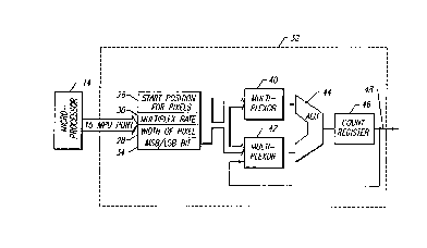
The control logic 32 is shown in additional detail
2 in Figure 2 and is indicated by broken lines in that Figure.
3 The register 26 indicating the start position of the first
4 pixel in the input buffer 23, the register 28 indicating the
pixel width and the register 30 indicating the multiplex rate
6 for separating each block into pixels are also shown in Figure
7 2. Figure 2 also indicates the register 34 for indicating the
F3 pixel display order in the block.
9
J.0 Figure 2 includes a multiplexer 40 which receives
indications from the register 28 in representation of the
12 width of each pixel as indicated in the register 28. Figure 2
also includes a multiplexer 42 which receives indications from
J,c~ the register 26 in representation of the start position of
16 each pixel in each block as indicated in the register 26. The
l~ outputs of the multiplexers 40 and 42 are introduced to an
J,~ arithmetic logic unit (ALUj 44. A connection is made from the
J,p output of the ALU 44 to the input of a shift count register
J,c~ 46. The output from the shift count register 46 is introduced
to an input to the multiplexer 42.
21
22 A start indication is introduced from the register
23 26 through the multiplexer 42 to one input of the ALU 44.
This input is used to set the shift register 46 to the start
position of the first pixel in the buffer 23. The second
2g pixel start position is computed when the multiplexer 4o then
2~ provides for the passage into the other input of the ALU 44 of
2g the number of bits corresponding to the width of each pixel.
29 The ALU adds or subtracts the two inputs and introduces the
result to the shift court register 46. The output from the
3J, shift count register 46 is introduced through a line 48 in
32 Figures 1 and 2 to the multiplexer 24 to control the operation
7
~~~~ r~
1 of the multiplexes in selecting each pixel in the block for
2 input to the single pixel buffer 25.
3
The third pixel is illustratively selected by first
switching the selected input of the multiplexes 42 from the
6 start position register 26 to the shift court register 46 when
7 it contains the start position of the second pixel. This
8 process is repeated until all pixels in the block have been
output to the buffer 25. The number of pixels to be output
].Q from each block is provided by the multiplex rate register 30.
11
Figure 4 indicates three blocks each having.a width
13 of sixty four (64) bits. The bit positions are indicated at
Z~, one end by a numeral "0" and at the other end by a numeral
yg "63". In Figure 4a, four pixels respectively designated as A,
],5 B, C and D are shown. Each pixel accordingly has a width of
sixteen (16) bits. The sequence of the pixels is in the order
],p A, B, C and D with the most significant bit in each pixel
Zg being at the left. In this sequence, the pixels are
2p multiplexed from the most significant bit of the block through
wl the bits of progressively decreasing significance.
22
In Figure 4b, the progressive pixels have the
24 sequence A, B, C, and D from the least significant bit at the
25 right toward the most significant bit at the left. In this
2g arrangement, the pixels multiplexed in the order A, B, C and D
27 from the least significant bit of the block at the right
2g toward the most significant bit at the left. Figure 4c shows
2g a block having eight (8) pixels each with eight (8) bits. The
p pixels have a sequence of A, B, C, D, E, F, G, H from the
31 least significant bit at the right. The pixels are presented
32 from the least significant bit at the right toward the most
8
1 significant bit at the left. It is not necessary for all of
2 the bits in the block to be used by a pixel. For example, if
3 the multiplex rate register 30 indicates that there are
i
s
x
4 (6) pixels in each block, only pixels A through F in the
previous example in this paragraph would be displayed before
6 moving to the next block.
7
f3 Each pixel contains a plurality of fields as shown
g in Figure 5. For example, each pixel may contain three (3)
fields respectively representing the primary colors red, green
~,l and blue. Each of these fields may have a number of bits to a
12 maximum of eight (8). Each pixel may also contain an overlay
~,3 field with a number of bits to a maximum of four (4). The
14 overlay field provides for an alternative pixel image from a
' s
~,~ separate pixel memory to be displayed over the pixel image
provided by the red, green and blue fields. Each pixel may
1'Y further include a cursor field with a number of bits to a
maximum of two (2). The cursor may be used to provide a
~,g pointer in the visual image. There also may be a field
containing a bypass control to a maximum of one (1) bit. The
21 bypass control provides a bypass of the palette random access
2 memory (RAM) and causes the information in the expanded color
fields to be output directly to a digital-to-analog converter
24 (DAC) 75.
26 Figure 3 illustrates a sub-system for separating and
2q scaling from each pixel the different fields shown in Figure
2g 5. The operation of Figure '3 for each field is controlled
~' 2g primarily by the start positions of each field as indicated in
a register 60. Only one register 60 is shown but it will be
31 appreciated that a number of such registers may be provided
,~ 32 each to indicate the start position of an individual one of
9
~~.p~ c~~
1 the fields in each: pixel. The start positions in the field
2 widths in the registers 62 are input to the register from the
3 microprocessor 14 through MPU port 15. Only one register 62
4 is shown but it will be appreciated that a number of such
registers may be provided each to indicate the width of an
6 individual one of the fields in each pixel. It will~also be
7 appreciated that the sub-system shown in Figure 3 processes,
F3 in a separate seguence, each.field such as shown in Figure 3.
9
Z.U The register 60 inputs the start position of each
11 particular field to control logic 64. The control logic 64
controls the operation of the shifter 66 in passing the
13 appropriate bits of information from the single pixel buffer
1~, 25 (also shown in Figure 1) to the particular field buffer 68.
The information passing to the field buffer 68 is preferably
16 in parallel form.
:~ ~r
lE3 The control logic 64 provides for the operation of
lg the shifter 66 in passing up to eight (8) positions from the
start position for each field. The number of positions passed
21 for each field is eight (8) for the red, green and blue
2 fields, four (4) for the overlay field, two (2) for the cursor
z3 field and one (1) for the bypass field. These eight (8)
2~ positions may include the particular field being separated
2~ from the pixel and may include bits in the next field or
26 fields.
~7
28 The register 62 contains the width of each field.
29 This information is introduced to control logic 70. Thus,
although eight (8) bits are stored in the field buffer 68,
31 only the number of bits in the field being processed are
32 passed as a result of the operation of the control logic 70.
to
1 The control logic 70 controls the expansian of the number
of
2 bits in each field to a particular number such as eight
; (8)
r
3 when the number of bits in such field is less than eight
(8).
4
The expansion of the number of bits in each field to
g eight (8) is performed by stages shown schematically as
q "scaling logic" 72 in Figure 3. Although the number of
bits
g stored in the field buffer 68 is eight (8) in the preferred
g embodiment, the scaling logic provides for the expansion
only
y0 of the bits in the field being processed at any instant.
For
11 example, if the number of bits in the field being processed
is
only six (6) bits, the scaling logic 72 operates only on
the
first six (6) bits from the buffer 68 and expands these
six
(6) bits to eight (8) bits.
Z6 The expanded number of bits in each field from the
1~ scaling logic 72 is introduced to a palette RAM 74 which
is
~,g known in the art. The palette RAM processes the indications
Zg in the different fields and introduces the processed
information to the video digital-to-analog converter (DAC)
21 which converts the binary indications to corresponding
analog
22 information. The analog information is then introduced
to a
23 video screen 76. The information in the different fields
in
24 each pixel controls the visual indications presented at
an
25 individual position on the video screen 76.
2g
27 Figure 7 indicates how the bits in a field are
t
2g expanded to eight (8j bits from a different numbers of
bits
2g less than eight (8) in such field. In Figure 7, the bits
in
30 the field after expansion are designated in the left column
by
!p;
,,
'' 31 the letter "R" and by numerals between "0" and "7". The
left
2 column is designated as "OUTPUT FIELD BIT". In this column,
11
1 the most significant bit is designated as "R7" and bits of
progressively decreasing binary significance are designated by
3 numerals of progressively decreasing value.
Figure 7 has a top row which is designated as
g "SOURCE FIELD WIDTH". This indicates the number of bits in
7 the field before expansion of the bits to eight (8). The row
~ below the designation of "SOURCE FIELD WIDTH" has numerical
g designations between "0" and "7". This indicates the number
of bits in the field before expansion. The designations in
11 the column below each of these individual numerical
;~~ designations between "0" and "7" indicate haw the pattern of
~,~5 the binary bits in the expanded field is obtained from an
individual number of binary bits in the field before
expansion.
Z7 In Figure 7, there are a number of indications in a
matrix relationship defined by eight rows to the right of the
g "OUTPUT FIELD BIT" column and eight columns below the numerals
in the row having the numerical designations "0" - "7" to
21 indicate the "SOURCE FIELD Width". This matrix has
designations between "RO" and "R7" in the cubicles defined by
the matrix. Some of these designations are in cubicles
24 without any cross hatching and others of these designations
are in crosshatched cubicles. As will be seen, the clear and
g cross hatched cubicles alternate in each column.
27
2g The unshaded desitlnations at the top of each column
2g in the matrix indicate the bits in the field being processed
before the number of bits are expanded to eight (8). For
31 example, in the column designated as "3", there are three (3)
bits in the field before expansion as indicated by three
12
~1~'~~
1 unshaded cubicles. These three (3) bits are respectively
2 designated as "R7", "R6°' and "R5" and are inserted into the
3 three (3) most significant binary positions in the field after
4 expansion. The three (3) bits are then repeated in the 4th)
5th and 6th cubicles of greatest binary significance in the
6 expanded field. To distinguish these bits from the bits of
7 greatest binary significance, the cubicles holding the bits
g "R7", "R6" and "R5" in the 4th, 5th and 6th most significant
g positions in the field after expansion are cross hatched. The
"R'1" and "R6" bits are then respectively inserted in the two
11 (2) cubicles of least binary significance. These cubicles are
lu not cross hatched to distinguish them from the adjacent cross
hatched cubicles in the column.
l~
As will be seen from Figure 7, there is a pattern
16 for expanding the number of bits in the field to eight (8).
1'~ The bits in the field before expansion are inserted into the
la positions of greatest binary significance in the expanded
Zg field. The unused positions in the expanded field are then
;gyp filled with the bits in the field before expansion. The
21 filling of unused positions in the expanded field with the
22 bits in the field before expansion may have to be repeated
more than once in order to fill all of the unused positions in
24 the expanded field. For example, when the number of bits in
the field before expansion is two (2), these bits have to be
2g repetitively used four (4) times to fill the positions in the
27 field after expansion. Furthermore, when the number of bits
2g in the field before expansion is not evenly divisible into
2g eight (8), all of the bits in the field before expansion are
3p not uniformly recorded in the field after expansion. For
31 example, when the number of bits in the field before expansion
32
13
.:
1 is three (3), only the bits R7 and R6, and not the bit R5, are
2 recorded in the least significant positions.
3
r
Figure 6 schematically indicates a subsystem for
operating upon the bits in the field before expansion to
6 obtain an expansion of the number of bits to eight (8). The
7 subsystem provides a plurality of input lines respectively
designated from left to right as "R7" to "RO". The lines R7-
9 RO are connected in individual patterns to multiplexers whose
J.0 outputs axe designated as "R6" progressively through "RO".
:L:L For example, the multiplexer which produces the bit R4 of the
expanded field receives the three (3) R7, R6 and R4 of
~,;5 information in the field before expansion and selects one of
these bits to become the R4 bit of the expanded field. The
bit R4 is selected for widths of four (4) through eight (8);
16 the bit R6 if the width if two (2); and the bit R7 is selected
for widths of one (1) bit and three (3) bits.
is
1~J Figure 8 is a chart showing the effectiveness of
filling the positions in each expanded field in the manner
21 shown in Figures 6 and 7 and described above. The first (1st)
column of Figure 8 shows progressive binary va.l.ues in a field
23 having only three (3) bits before expansion, the least
2~ significant bit being shown at the right. These three (3)
2~ bits are recorded in the positions of greatest binary
Q6 significance in the expanded field of eight (8) bats. The
~~7 second (2nd) column in Figure 8 shows the percentage that the
,?8 bits shown in column 1 have to a full count in the field
before expansion. This full count is represented by a binary
30 pattern of 111 constituting the maximum capable of being
31 recorded in the field before expansion.
3~
14
~~.~~'~3~
The third (3rd) column in Figure 8 indicates the
2 pattern of the bits recorded in the five (5) positions of
3 least binary significance in the field after the expansion of
4 the field to eight (8) bits. In the third (3rd) column of
Figure 8, the least significant bit is at the right. The
6 pattern of the bits recorded in the five (5) positions of
7 least binary significance corresponds to the pattern shown in
8 Figure 7 in the column designated as "3". The fourth (4th)
9 column of Figure 8 shows the pattern of bits in the eight (8)
positions in the expanded field. In the fourth (4th) column
i.l of Figure 8, the least significant bit is at the right.
12
13 , The fifth (5th) column of Figure 8 indicates the
percentage of the value of the binary bits in the field after
expansion, as indicated by the bir;ary bits in the fourth (4th)
],6 column of Figure 8, relative to the full value of such field
17 as indicated by a binary value of "1" for each bit. The sixth
la (6th) column of Figure 8 shows the difference in the
lg percentages between the values in the second (2nd) and fifth
(5th) columns. A positive value in the sixth (6th) column
21 indicates that the value in the second (2nd) column exceeds
22 the value in the fifth (5th) column. A negative value in the
23 sixth (6th) column indicates that the value in the second
2c~ (2nd) column is less than the value in the fifth (5th) column.
2fi In order to obtain a complete accuracy in the
27 expansion of each field to eight (8) bits, the differences
28 between the values in the second (2nd) and fifth (5th) columns
29 should not exceed one half (1/2) of the value of the least
significant bit in the expanded field. This is a value of
31 approximately two tenths of one percent (0.2%) of the full
3? scale value. Any relative error less than this percentage of
~1~~"~~~
1 two tenths of one percent (0.2%) in a field will not affect
any output indications in a pixel position since it will not
3 affect the value of the least significant bit in the expanded
ffield.
6 As will be seen, each of the errors shown in the
7 sixth (6th) column of Figure 8 has a value less than two
g tenths of one percent (0.2%). If the same process as
g described above and shown in Figures 6-8 is used to determine
1.0 the error when any binary value less than eight (8) bits is
1~) expanded to eight (8) bits, it will be seen that the error
resulting from such expansion is less than two tenths of one
13 percent (0.2%)
i~
The apparatus and method described above have
Z~ certain important advantages. A universal system is provided
l~ for processing pixels regardless of (a) the width of the
lp blocks, the pixels in the blocks and the fields in the pixels,
yc~ (b) the presentation of the bits in the blocks, pixels and
fields from the most significant position or the least
21 significant position and (c) the start position of each block,
position and field. Furthermore, each field is provided with
a particular number of bits such as eight (8). This
24 simplifies and facilitates the processing of the information
in each field. The expansion of the bits in each field to
eight (8) occurs in a pre-selected relationship in which no
error is produced as a result of the expansion.
29
31
J
16
~~.~~?~
Although this invention has been disclosed and
2 illustrated with reference to particular embodiments, the
3 principles involved are susceptible for use in numerous other
4 embodiments which will be apparent to persons skilled in the
art. The invention is, therefore, to be limited only as
6 indicated by the scope of the appended claims.
io
:L J.
i2
~.5
~. J
m
17
~~
~9
27.
22
23
24 '
26
27
2~
29
~i
i 31
i
I
I 32
17