Note: Descriptions are shown in the official language in which they were submitted.
21~8~S7
BACKGROUND OF THE INVENTION
Field of the invention
This invention relates to the field of
COMINT/ELINT (communications intelligence/electronic
intelligence) signal processing, and more particularly to
a circuit with which very low-level to moderate-level
signals can be detected, without any a priori
information, while other stronger signals are present and
transmitting close to the instantaneous frequency of the
desired signal.
Backqround Art
Reference is made to U.S. Patent No. 4,965,581
entitled, "Real Time Rejection Circuit to Automatically
Reject Multiple Interfering Hopping Signals While Passing
A Lower Level Desired Signal" by W. Skudera & S. Albert,
issued October 23, 1990 (hereinafter "the '581 patent").
Reference is also made to a paper entitled "SAW
Tapped Delay Lines for New Potential Circuit
Applications" by William J. Skudera, Jr., which was
published in approximately September 1988 in the
Proceedings of the 42nd Annual Frequency Control
21 08957
Symposium 1988, IEEE Catalog No. 88CH2588-2, Library of
Congress No. 58-60781 (hereinafter "the 1988 article"); and to
Canadian Patent 2,109,049, by William J. Skudera, Jr., titled
"Sequential Circuitry for Recreating CW Components from Chirp-
Z Pulses" which issued on 16 April 1996.
The just-cited patent and the 1988 article describe
several embodiments of circuits which use a tapped delay line
in an amplifier feedback loop circuit to replace the inverse
transform of a chirped Fourier transform processor for CW
input signals. The conventional inverse transform processor
loses on the order of 20-30 dB of the processing gain achieved
by the forward processor. However, the described circuit can
be utilized to recirculate the signal in order to recreate a
continuous CW signal from the transform signal.
In addition, reference is made to Fig. 2 of co-
pending Canadian Patent Application no. 2,092,125 filed March
22, 1993 in the names of Stuart D. Albert and William J.
Skudera, Jr. entitled, "Apparatus and Method for Real Time
Interference Signal Rejection".
Conventional methods have failed to achieve
detection of very weak desired signals under adverse
conditions and without a Priori information about the
received signals, because such detection requires a circuit
with both ultra-wide dynamic range and very high signal
sensitivity. The receiver must be able to receive
moderate- to very-low-level signals without becoming
21n8,~57
saturated and therefore being made inoperable by the
strong signals.
SUMMARY OF THE INVENTION
These and other objects are satisfied by a wide
dynamic range detection circuit for detecting low-level
desired signals in the presence of nearby strong
interfering signals, comprising receiving means for
receiving electromagnetic signals including at least a
desired signal and a strong interfering signal on a
nearby frequency; attenuating means for attenuating the
interfering signal to a given degree while attenuating
the desired signal to a substantially lesser degree;
first chirp-Z processing means for receiving the output
of the attenuating means and producing respective chirp-Z
transforms of the desired and interfering signals;
modulating gate means which receives the output of the
first chirp-Z processing means and is responsive to the
chirp-Z transform of the interfering signal, for
selectively blocking the interfering signal transform
while passing the desired signal transform; and first
detecting means for detecting the desired signal
transform and generating an output indicative of such
detection.
The attenuating means may comprise a frequency-
selective YIG filter and/or a programmable notch filter,
for example.
The modulating gate means may comprise one or
two modulator gates which block the chirp-Z transform of
the interfering signal and pass the chirp-Z transform of
the desired signal. The modulator gates may be
responsive to the interfering signal transform produced
by the first chirp-Z processing means, or to an
~In.~s7
interfering signal transform produced by a second chirp-Z
processing means.
The detecting means may comprise a peak
detection circuit and/or a recirculation loop for
recreating the desired signal from the chirp-Z transform
of the desired signal. A second detecting means may be
provided for detecting the interfering signal transform
and generating an output indicative of such detection.
The second detecting means may comprise a peak detector
circuit. Summing means may be provided for receiving and
summing the outputs of the first and second detecting
means and generating a summed output.
The disclosed embodiments of the invention
provide circuits which are capable of receiving and
detecting very-low-level and moderate-level desired
signals, while at the same time removing unwanted high-
power interference signals. The circuits further are
able to operate over a wide instantaneous band-width and
are able to handle multiple simultaneous signals.
More specifically, in the second embodiment of
the invention, the sensitivity of the passive chirp-Z
transform is increased by 30 dB, to a value of -120 dBm,
over a substantial bandwidth, for example 50 MHz. The
second embodiment is capable of operating accurately in
the presence of +10 dBm signals while maintaining a
sensitivity of -110 dBm, thus achieving an effective
dynamic range of 120 dB. The second embodiment is
further capable of handling and characterizing the
interference signal separately, if its signal
characterization is desired.
Other features and advantages of the present
invention will become apparent from the following
21Q~57
description of the invention which refers to the
accompanying drawings.
BRIEF DESCRIPTION OF THE DRAWINGS
Figs. lA and lB are respectively a schematic
block diagram of a first embodiment of the invention, and
a diagram showing signal levels at various points within
the first embodiment; and
Figs. 2A and 2B are respectively a schematic
block diagram of a second embodiment of the invention,
and a diagram showing signal levels at various points
within the second embodiment.
DETAILED DESCRIPTION OF EMBODIMENTS OF THE INVENTION
First Embodiment
Fig. lA shows a circuit which is capable of
improving the effective dynamic range of a chirp-Z
processor by up to 30 dB by utilizing a frequency
selective type filter, such as a YIG filter, which limits
only high-power signals by a factor of the order of 30 dB
or more, while allowing lower level signals to go through
essentially unaffected. Such a filter is placed before
the chirp-Z processor described in the '581 patent, which
allows the chirp-Z processor to operate at reasonably low
sensitivity level without becoming saturated by high-
level signals. The operation of the YIG limiting filter
is well known per se, and is described in an article
entitled, "Application of YIG Devices" by J. McCole and
A. Shaw, in Microwaves, September 1965.
Fig. lB schematically shows an example of
signals which are handled by the circuit of Fig. lA. In
Fig. lB, a strong signal S1, whose signal strength could,
for example, be in the range of -30 to +10 dBm, is shown
21n8.~s7
attenuated to -30 to -20 dBm by the YIG filter, while the
desired signal S2 is shown unaffected, although in
practice there may be 1 to 2 dB of insertion loss. The
desired signal usually has a low signal strength that
usually is well below the -30 dBm level because of the
typical transmitting distances involved.
After going through the chirp-Z processor both
signals are enhanced by the order of 30 dB.
Then signals Sl and S2 are both passed through
a pair of modulator gates Gate 1 and Gate 2. As
discussed in the '581 patent, each modulator gate blocks
the time-domain pulses that represent the chirp-Z
transform of the strong interfering signal, but passes
the chirp-Z transform of the low-level desired signal.
Each gate therefore has the effect of lowering the S1
signal without affecting the S2 signal. For example,
Gates 1 and 2 may each lower signal S1 by approximately
30 dB. Thus, after the two gates, the desired signal S2
is well above the interference signal Sl. Signal S2 can
then be detected using a standard peak detector circuit,
or if the signal is modulated, it can be supplied to a
recirculation loop, as explained in the 1988 article, for
recreation of the original S2 signal.
The circuit of Fig. lA, therefore, effectively
achieves an excellent dynamic range of 90 dB.
A S/N ratio of 6-10 dB is generally considered
to be preferable for producing a good output signal.
Therefore, to achieve a more useful dynamic range, the
lower input range of signal S2 advantageously would be
increased by 10 dB to -70 dBm to yield a minimum S/N of
10 dB (the minimum S2 to the noise level), or a useful
dynamic range of 80 dB, over a bandwidth, for example, of
50 MHz.
2lQ~2i~J7
Second Embodiment
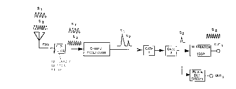
Fig. 2A shows a circuit that extends the
effective operational dynamic range to 120 dBm via a two-
channel arrangement. A first channel CH1 receives the
interference signal (Sl in this example), which is
considered to be a high-level signal (-50 to +10 dBm),
and the desired signal S2. After processing by a
resistive attenuator ATTN, only the interference signal
S1 remains above the sensitivity level Smin. of the
chirp-Z processor. The other channel CH2 is protected
from the high-level signal by both a YIG filter and a
programmable notch filter circuit Thus the signal Si is
substantially reduced, while the desired signal S2 is
substantially unaffected.~
After the attenuator ATTN in channel CH1, the
signal S1 is supplied to chirp-Z processor C1 which
outputs a pulse-like transform, as is well known.
The chirp-Z processor C2 in the second channel
CH2 receives the signals S1 and S2 from the notch filter
and outputs a corresponding pair of pulse-like transform
signals.
The processor C2 can be optimized to receive
very low signals, from -120 to -60 dBm, via the use of a
proper amount of gain in the circuit, since it can have
resolution of the order of 20 kHz and is, therefore,
approximately equivalent to a narrow band circuit. This
is shown by equation (1) below:
Smin.= -114 dBm (KT level for 1 MHz) +
10 log (BW) + NF - PG (1)
-- 7 --
2 ~ 7
wherein: KT is the thermal noise floor,
BW is the RF bandwidth in MHz,
NF is the noise figure of the circuit, and
PG is the processing gain of the dispersive
filter used in the chirp-Z processor.
For example, if one uses typical values for the above
equation, such as: NF = 3.0 dB, BW = 50 MHz, and PG =
lO*Log(T*BW), where T = 50 us, then Smin. = -114 + 17 + 3
-34 = -128 dBm. By comparison, a standard narrow-band
(20 kHz) receiver would obtain approximately the same
Smin., referring to equation (1), with PG = zero because
dispersive filters could not be employed, and because
lO*log(.020) = -17 dB.
It is further to be noted that 6 to 10 dB
should be allowed for pulse detection/threshold, although
this was omitted from equation (1), and that other
component losses were assumed to be negligible.
Therefore, in practice, the Smin. could be of the order
of 10 dB less. In addition, equation (1) assumes an
input signal duration equal to or greater than the SLO
(sweeping local oscillator) period of the chirp-Z
processor to achieve a maximum processing gain.
It is further to be noted that in Fig. 2B an
Smin. value of -110 is shown instead of -120. The reason
for using the higher value is that YIG filters generally
limit between -20 to +10 dBm. Therefore, if one wanted
the dynamic range to extend from -120 to 0 dBm, then a
second notch filter could be utilized in place of the YIG
filter.
The output from the chirp-Z processor Cl in
channel CH1, which is the chirp-Z transform of the
interference signal S1, is used to control the notch
21 08957
filter. The notch and YIG filters reduce the signal S1
entering the chirp-Z processor C2 in channel CH2 by a total of
60 dB. Then, the two modulator gates Gate 1 and Gate 2 reduce
the S1 signal from processor C2 by another 60 dB, as explained
in the '581 patent, with negligible effect on signal S2.
However, in this case the gates are controlled "OFF" by the
signal Sl from the chirp-Z processor Cl, as opposed to an
automatic-type control scheme as disclosed in the '581 patent.
After passing through Gate 2, the transform of the
desired signal S2 can be converted to a CW-type signal via
the re-creation loop as explained in the 1988 article or in
Canadian Patent 2,109,049 in the name of William J. Skudera,
Jr., titled "Sequential Circuitry for Recreating CW components
from Chirp-Z Pulses," and then provided to output OUT4.
Alternatively, the transform signal S2 could be detected via
a standard peak-detection-type circuit (PEAK DET. CIRCUIT 2
in Fig. 2A), whose output is then provided to output 3.
In addition, as shown in Fig. 2A, one can peak-
detect both channels (see PEAK DET. CIRCUIT 1) and either
look at the outputs separately (outputs OUT1 and OUT3,
respectively) or combine them in a summer (~) which has
output OUT2. Thus, if the receiver is dealing with a single
input signal, then output OUT2 will yield a continuous
120 dBm range.
If one wants to characterize the interference
signal S1 separately, then OUT1 is utilized. If just
the desired signal S2 is to be detected, then output OUT3
is used. Also, if a CW version of the desired
~IJ _ 9 _
2ln/~.s~7
signal S2 is required, then output OUT4 is used, wherein
the signal goes through the recreation loop described in
the 1988 article.
It is to be noted that the function of the
three delay lines shown in Fig. 2A is to keep the signals
tracking in the two channels and through the two gates.
The signal sketches drawn in Fig. 2A, and the
signal power levels of each signal shown in Fig. 2B at
various locations along channel CH2, are utilized only to
simplify the explanation of the circuit operation and are
not intended to limit the scope of the invention.
Although the present invention has been
described in relation to particular embodiments thereof,
many other variations and modifications and other uses
will become apparent to those skilled in the art. It is
preferred, therefore, that the present invention be
limited not by the specific disclosure herein, but only
by the appended claims.
-- 10 --