Note: Descriptions are shown in the official language in which they were submitted.
- 2109:L33 --
MULTIPLE-LAYER MICROSTRIP ASSEMBLY WITH
INTER-LAYER CONNECTIONS
Backqround of the Invention
1. Field of the Invention
This invention relates to a multiple-layer microstrip
or stripline assembly and, more specifically, to
transitioning electrical signals between two or more
separate layers. A microstrip is a type of waveguide
comprising a conductor, typically in a flat, rectangular
shape, separated from a single ground plane by a dielectric
substrate material. ~ buried microstrip is a variation on
the basic microstrip wherein the single conductor is
embedded in a dielectric substrate material. A stripline
is similar to a buried microstrip, except that a stripline
has two ground planes -- one located along each major
surface of the dielectric substrate material.
2. Description of the Related Art
Many systems utilize multiple-layer microstrip
assemblies in which various circuit elements are sandwiched
between separate layers of dielectric material and
laminated together to form a single composite structure.
The types of various circuit elements to be used may
include both passive and active components, as well as
transmission lines (equivalently referred to as feedlines).
One reason for using multiple-layer construction is to
avoid electromagnetic interference between the signals
present in the feedlines and circuit elements by isolating
them from one another. In one frequently used
-` 21~:L33
configuration, the feedlines are arranged on the top
surface of the bottom-most layer, separated by a dielectric
substrate material from a ground plane located on the
bottom surface of the bottom-most layer, while the various
other circuit elements are distributed among the upper
layers of the assembly.
When the feedlines and circuit elements which comprise
a system are distributed over a plurality of separate
layers, however, it becomes necessary to route signals back
and forth between different layers to interconnect the
various circuitry. For example, to implement a certain
circuit function it may be necessary to connect a feedline
on a first layer to a circuit element on a second layer.
Additionally, it may be necessary to route several signals,
originating on different layers, to appear on a single
layer to facilitate connection to an external device.
The routing of signals between layers, however,
presents problems. First, the process of constructing a
microstrip assembly with inter-layer connections is time
and labor intensive and burdensome due to the low
tolerances for error. A known technique for constructing
a multiple-layer microstrip assembly with inter-layer
connections requires several steps as described below with
reference to FIGS. lA through lE.
As illustrated in FIG. lA, a ribbon 101 is connected
by means of soldering to first top circuitry 103, for
example, a circuit element or feedline, on a first layer
105.
21~9~33
Next, as shown in FIG. lB, a second layer 107 must be
brought into precise alignment with the first layer 105
such that the ribbon 101 may be passed through a hole 109
in the second layer 107. The task of aligning layers and
feeding-through connecting ribbons requires a great deal of
precision and is aggravated by the fact that, typically,
several connections between the two layers, with each
requiring a ribbon and alignment with a hole, must
typically be made between the two layers.
As shown in FIG. lC, the first layer 105 is then
joined to the second layer 107 by means of a first laminate
layer 111 therebetween. The first laminate layer 111 holds
the ribbon 101 in a fixed position relative to the hole 109
in the second layer 107 and prevents disturbing the precise
alignment achieved in the step performed as shown in FIG.
lB.
Next, as shown in FIG. lD, the ribbon 101 passing
through the hole 109 in the second layer 107 is connected
by means of soldering to second top circuitry 113, for
example, a circuit element or feedline, on the second layer
107. The ribbon 101 forms an ohmic electrical connection
between the first top circuitry 103 on the first layer 105
and the second top circuitry 113 on the second layer 107
and completes the structure necessary to transition signals
between analogous surfaces of two separate layers of a
multiple-layer microstrip assembly.
Finally, as shown in FIG lE., an optional second
laminate layer 115 may be disposed on top of the second
2 ~ 3 ~
layer 107 to cover the second top circuitry 113. The
second laminate layer 115 insulates the second top
circuitry 113 from unwanted ohmic short-circuits and holds
the ribbon 101 firmly in position.
Although the above-described construction method
provides a multiple-layer microstrip assembly capable of
transitioning signals between separate layers, it has
several drawbacks. Among the drawbacks, the prior method
is time and labor intensive due to the need for a precise
alignment step. Furthermore, the prior method presents a
low tolerance for error due to the difficulty in aligning
the small-sized hole and ribbon. Additionally, because the
above-described structure requires a ribbon to be connected
between two separate layers, the ribbon is subject to
stress, possibly causing failure or an impedance mismatch,
from any relative movement between the two layers during
construction.
Another problem associated with routing signals
between layers is that the interconnections may result in
degradation of the signal due to reflections caused by
impedance mismatches. It is for this reason that a prior
multiple-layer microstrip assembly with inter-layer
connections was likely to have diminished radio-frequency
(RF) performance as compared to a single-layer microstrip
25 assembly which did not require inter-layer connections. `~
Clearly, an apparatus and construction method for
multi-layer microstrip assemblies that addresses these
deficiencies is desirable.
2 ~ 3
Summary of the Invention
It is an object of the present invention to provide a
multiple-layer microstrip assembly with means for
transitioning signals between analogous surfaces of two
separate layers thereof.
It is also an object of the present invention to
provide an improved method of constructing the above-
mentioned multiple-layer microstrip assembly.
It is a further object of the present invention to
provide an inter-layer connection for a multiple-layer
microstrip assembly which provides RF performance
comparable to that of a single layer assembly.
It is a further object of the present invention to
provide a method of constructing~ a multiple-layer
microstrip assembly with a reduced number of steps.
It is a further object of the present invention to
provide a method of constructing a multiple-layer
microstrip assembly wherein the interconnection of two pre-
assembled layers may be completed by a single step of
~oining the two layers together.
The foregoing and other objects are achieved by
joining a first layer that has circuitry on its top surface
electrically connected to circuitry on its bottom surface,
with a second layer that has circuitry on its top surface,
wherein the circuitry on the bottom surface of the first
layer overlaps the circuitry on the top surface of the
second layer to form an electrical connection therebetween.
Consequently, a signal transition between the top surface
2 ~ 3 3
of the first layer and the top surface of the second layer
is provided.
In one embodiment, th~ overlapping electrical
connection is established by juxtaposing the first and
second layers so that the circuitry on the bottom of the
first layer is capacitively coupled to the circuitry on the
top of the second layer.
In yet a further embodiment of the invention, the
electrical connection between the circuitry on the top and
bottoms of the first layer is accomplished by establishing
a hole between the top and bottom, and then electrically
connecting the top and bottom circuitry with an electrical
connector that extends through the hole.
These and other features of the present invention will
become evident from the detailed description set forth
hereafter with reference to the accompanying drawings.
Brief Description of Drawinqs
A more complete understanding of the invention can be
had by referring to the detailed description of the
invention and the drawings in which:
FIGS. lA-lE are side assembly views of the five steps
of a known method for constructing a multiple-layer
microstrip assembly with an inter-layer connection.
FIG. 2A is a side view showing the interconnection of
two layers of a microstrip assembly in accordance with one
embodiment of the present invention.
21~9:~3
FIG. 2B is a top view of the apparatus shown in FIG. .:
2A. :
FIG. 2C is an enlarged view of the Region AA from FIG.
2B.
FIG. 3 is an exploded perspective view of the
microstrip assembly illustrated in FIG. 2A.
FIG. 4 is a top view of an overlap connection
according to another embodiment of the present invention.
FIG. 5 is a top view of an overlap connection
according to another embodiment of the present invention.
FIGS. 6A-6D are side assembly views of the four steps
of a method for constructing a microstrip assembly with an
inter-layer connection according to the present invention.
De~ailed Description of the Invention
A detailed description of a multiple-layer microstrip
assem~ y adapted to transition electrical signals between
analogous surfaces of two layers thereof, and a method of
constructing the assembly, is set forth below with
reference to the figures.
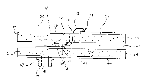
Referring to FIGS. 2A-3, the multiple-layer microstrip
assembly according to one embodiment of the present
invention illustrated therein comprises a first layer 10
and a second layer 12. The first layer 10 has a first top
surface 14 and a first bottom surface 16 substantially
parallel to the first top surface 14, separated by a first
edge surface 18. Similarly, the second layer 12 has a
second top surface 20 and a substantially parallel second
21~9:L33
bottom surface 22, separated by a second edge s~lrface 24.
Each of the first layer 10 and the second layer 12 is
composed of a suitable dielectric material.
Disposed on the first top surface 14 of the first
layer 10 is first top circuitry 26, and disposed on the
first bottom surface 16 of the first layer 10 is first
bottom circuitry 28. Each of the first top circuitry 26
and the first bottom circuitry 28 may comprise, for
example, a circuit element, a feedline, printed circuitry,
or a combination thereof. In this particular embodiment,
the first layer 10 has a hole 30 connecting the first top
surface 14 and the first bottom surface 16. The hole 30
has an appropriately sized diameter such that an
electrically conductive member 32, for example, a wire or
a ribbon, may pass therethrough. Alternatively, the hole
30 can be plated with an electrically conductive material
or an electrically conductive eyelet can be established in
the hole 30. The electrically conductive member 32 is
comprised of appropriate conductive material to establish
an electrical connection between the first top circuitry 26
and the first bottom circuitry 28.
As an alternative to using the electrically conductive
membor 32 to connect the first top circuity 26 to the first
bottom circuitry 28, these two sets of circuitry may be so
constructed as to form a single unitary member rather than
distinct sets of circuitry with a separate connection means
therebetween. This may be accomplished, for example, by
plating the first layer 10 to establish the first top
~?f:~
2~Q~33
circuitry 26 and the first bottom circuitry 28, and at the
same time plate the hole 30 to establish an electrical
connection between the first top circuitry 26 and the first
bottom circuitry 28.
As shown, the electrically conductive member 32 is
positioned within the hole 30 such that one end of the
electrically conductive member 32 abuts the first top
circuitry 26 and the other end of the electrically
conductive member 32 abuts the first bottom circuitry 28 at
attachment points 34. The electrically conductive member
32 is attached, for example, by a solder joint. The
attachment of the electrically conductive member 32 at
attachment points 34 forms an ohmic electrical connection
between the first top circuitry 26 and the first bottom
circuitry 28.
According to the embodiment of the present invention
as illustrated in FIGS. 2A-3 an optional first laminate
layer 36 comprising, for example, a resin material having
suitable dielectric and bonding characteristics, is
disposed on top of the first top surface 14 of the first
layer 10. The purpose of the optional first laminate layer
36, inter alia, is to electrically insulate the first top
circuitry 26, and to secure each of the first top circuitry
26 and the electrically conductive member 32 in place.
Disposed on the second top surface 20 of the second
layer 12 is second top circuitry 38. The second top
circuitry 38 may comprise, for example, a circuit element,
a feedline, printed circuitry, or a combination thereof.
210~3~
A ground plane 37 is arranged along the second bottom
surface 22 of the second layer 12. An input connector 43,
for example, a coaxial connector -- comprising a housing 39
and a feed pin 41 -- is attached to the ground plane 37
such that the housing 39 is physically and electrically
connected to the ground plane 37, while the feed pin 41, or
signal carrying line, passes through a gap in the ground
plane 37 into the dielectric substrate material comprising
the second layer 12, to physically and electrically connect
to the second top circuitry 38, for example, by means of
soldering.
The first layer 10 and the second layer 12 are
oriented such tha' the first bottom surface 16 of the first
layer 10 faces opposite the second top surface 20 of the
second layer 12. The second top circuitry 38 is positioned
adjacent and overlapping with the first bottom circuitry
28.
An electrical connection exists between the second top
circuitry 38 and the first bottom circuitry 28 in the
overlap region 40 by means of capacitive coupling between
the two sets of circuitry. Capacitive coupling provides a
reliable and easy method for establishing an electrical
connection between the two sets of circuitry. If certain
requirements are met, as discussed below, a capacitively
coupled electrical connection performs comparably to an
ohmic electrical connection. Moreover, the capacitively
coupled connection is established merely by bonding the two
sets of circuitry in an adjacent and overlapped position
~:~a~v.~3
using a lamination layer of suitable bonding and dielectric
properties. Because no physical connection need be
maintained between the two sets of circuitry to establish
a capacitively coupled connection, the reliability of the
assembly is enhanced.
Another possible embodiment with a different means of
forming an electrical connection between the two sets of
circuitry involves bringing the first bottom circuitry 28
into physical contact with the second top circuitry 38 such
that an ohmic electrical connection, rather than a
capacitively coupled electrical connection, is formed
therebetween. Typically, such a connection, however,
involves a greater degree of difficulty in construction
because the two sets of circuitry to be electrically
connected must be held in constant physical contact to
ensure a stable electrical connection. For example, to
establish an ohmic electrical connection between the first
bottom circuitry 28 and the second top circuitry 38 in the
microstrip assembly illustrated in FIG. 2A, it would be
necessary to laminate the first layer lO to the second
layer 12 such that the first bottom circuitry 28 was held
in constant physical contact with the second top circuitry
38 with no laminate material in between the two sets of
circuitry.
In the embodiment of the present invention shown in
FIG. 2A utilizing capacitive coupling, the characteristics
of the resultant capacitively coupled electrical connection
are determined by several parameters. Initially, when
..... ... `. .. ........ `.. ;,.. ,.,.. ~,',.~ i.. ~
2la~.~33
operating at higher frequencies, such as in the RF range,
it is important that interconnections between circuit
elements be impedance matched to minimize signal
reflections and maximize~power transfer. One method to
achieve an impedance matched connection is to create an
overlap length of A/4 between the two sets of circuitry.
As shown in FIG. 2A, the overlap length, V, of this
embodiment is substantially equal to A/4 thereby
establishing an impedance matched electrical connection.
Alternatively, the overlap length, V, may be equal to
a length other than A/4 as long as the overlapped surface
area establishes sufficient capacitive coupling between the
first bottom circuitry 28 and the second top circuity 38.
For example, an overlap length other than A/4 may be
desirable for systems which operate over a broad band of
frequencies and not just RF frequencies.
The capacitance of the connection, C, is determined by
the equation:
(i) C = ~A/d
where ~ is the dielectric constant of the material in
between the two sets of circuitry, A is the surface area of
the overlapped region, and d is the separation of the two
sets of circuitry. The impedance of the connection, Z, is
determined by the equation:
(ii) Z = -j/wC
where -j is equal to the square-root of -1, ~ is equal to
2~ times the frequency, and C is the capacitance of the
connection, calculated according to equation (i), above.
~ 2~0~33
When appropriate values of ~, A, and d are used, the
capacitance, c, is great enough so that the impedance, Z,
of the connection becomes negligible and the connection
effectively appears as a short-circuit to RF signals.
Referring to FIG. 2C, a top view showing the overlap
region 40 between the first bottom circuitry 28 and the
second top circuitry 38 is illustrated. As shown, one of
the two sets of circuitry, in this case the second top
circuitry 38, is slightly narrower, by an amount ~, than
the width of the first bottom circuitry 28, X + ~. The
purpose of the difference in width, ~, is to provide a
registration tolerance when constructing the apparatus of
the present invention. More particularly, to ensure that
the second top circuitry 38 sits entirely underneath the
first bottom circuitry 28 within the overlap region 40, the
second top circuitry 38 is slightly narrower to provide the
necessary registration tolerance when constructing the
microstrip assembly of the present invention.
Because the width of a feedlir.~ is inversely
proportional to its characteristic impedance, the second
top circuitry 38, taken alone, would have a characteristic
impedance greater than the first bottom circuitry 28, taken
alone, by an amount proportional to the difference in
width, ~. When the two sets of circuitry are coupled in
the manner described above, however, the characteristic
impedance of the aggregate structure -- that is, the two
sets of circuitry combined -- is determined solely by the
13
-- 21~9~3
width of the wider of the two sets of overlapping circuitry
-- in this case, the first bottom circuitry 28.
In the particular embodiment of FIGS. 2A-3, the second
top circuitry 38 is held adjacent and overlapping with the
first bottom circuitry 28 by means of a second laminate
layer 42 to ensure an electrical connection during
operation of the microstrip assembly. Although a laminate
layer is used in this embodiment, alternative means, such
as a support frame, clamps, screws, or springs, may be used
to hold the first layer 10 and the second layer 12
together.
An alternative embodiment with a different arrangement
for the overlap of the two sets of circuitry, providing
even greater registration tolerance, is~illustrated in FIG.
4. In the particular embodiment depicted therein, each of
the first bottom circuitry 228 and the second top circuitry
238 have a width X. The first bottom circuitry 228,
however, has a terminal end 230, in the shape of a stub,
with a width W significantly greater than X. The overlap
configuration in the embodiment illustrated in FIG. 4 is an
exception to the general rule that the width of wider of
the two sets of circuitry determines the characteristic
impedance of the aggregate coupled circuitry. In this
embodiment the value of the width W is irrelevant with
respect to the characteristic impedance of the overlapped
circuitry. As long as the overlap length, Vl, is
substantially equal to A/4, and the length, V2, of the
terminal end 230 is substantially equal to l/2, the
14
-~ 21~:l33
characteristic impedance of the overall structure -- that
is, the first bottom circuitry 228 overlapped with the
second top circuitry 238 -- is determined by the width X.
Therefore, a value of W should be chosen such that adequate
registration tolerance is provided in the overlap region
240. This embodiment has the advantages of providing ample
registration tolerance while maintaining a consistent
width, X, between the two sets of circuitry.
Still another embodiment of the present invention,
which takes advantage of the structure of a branch-line
quadrature hybrid circuit to form the overlapping
electrical connection of the two sets of circuitry, is
illustrated in FIG. 5. A branch-line quadrature hybrid
circuit element is used to divide the power of an input
signal among one or more output signals as well as to
supply one or more output signals with phase differences,
relative to the input signals, that are multiples of 90.
These phase differences are achieved by separating an input
port that provides the input signal from an output port
that provides an output signal by a transmission line that
is A/4 in length or a multiple thereof. In this embodiment
the second top circuitry 338, represented by dashed lines,
forms a first portion of a branch-line quadrature hybrid
circuit. The first bottom circuitry 328, represented by
solid lines, forms a second portion of the branch-line
quadrature hybrid circuit. The first bottom circuitry 328
overlaps the second top circuitry 338 in the overlap
regions 340 wherein a capacitively coupled electrical
-~ 2.~ 3 3
connection is established. The resulting structure formed
by the overlap of the first bottom circuitry 328 and the
second top circuitry 338 is referred to as a branch-line
quadrature hybrid. This device has four ports 346 and is
used, inter alia, for dividing power and supplying
different phase outputs. In the branch-line quadrature
hybrid, the length of each of the shunt arms 344 (the U-
shaped portions) and the series arms 342 (the connecting
portions) is substantially equal to A/4. Additionally, the
shunt arms 344 are wider, and therefore have a lower
characteristic impedance, than each of the series arms 342
and the four ports 346.
The establishment of the overlapping, electrical
connection between the first bottom circuitry 328 and the
second top circuitry 338 using the branch-line quadrature
hybrid structure provides several advantages.
Specifically, the U-shaped portions provide a convenient
location for the overlap of the two sets of circuitry to
occur for the following reasons. First, the shunt arms
344, already having increased width for reasons of circuit
operation, also provide the necessary registration
tolerance for the overlap between the two sets of
circuitry. As discussed above, the characteristic
impedance of the overall shunt arm structure -- that is,
the overlap regions 340 formed by the respective U-shaped
portions of the first bottom circuitry 328 and the second
top circuitry 338 -- is determined by the wider of the two
sets of circuitry, in this case, the second top circuitry
16
3 ~ :
338. Consequently, the narrower width of the U-shaped
portions of the first bottom circuitry 328 have little, if
any, effect upon the RF performance of the hybrid.
Second, because the shunt arms 344 of the branch-line
quadrature hybrid are already substantially equal to A/4 in
- length for reasons of circuit operation, having the two
sets of circuitry overlap in the U-shaped portions provides
an over].ap length substantially equal to A/4, thereby
ensuring an impedance matched electrical connection which
effectively appears as a short-circuit to RF signals. The
shunt arms 344, having the properties of both increased
width and a A/4 length are, therefore, a highly
advantageous location for the overlap of the two sets of
circuitry to occur in providing a transition for signals
between the first and second layers.
Finally, because the first bottom circuitry 328 can be
made narrower than the second top circuitry 338, two of the
four ports 346 that are part of the first bottom circuitry
328 are narrower than the shunt arms 344 as required for
proper operation of the hybrid.
It is important to note that the circuit elements and
feedlines in the above-described embodiments must maintain
the characteristics of a microstrip transmission line. As
mentioned previously, a microstrip transmission line
comprises a signal conductor separated from a single ground
plane only by a dielectric material. Therefore, in each of
the above-described embodiments there is no overlap between
the first top circuitry and the combination of the first
21 ~9133
bottom circuitry and the second top circuitry. In other
words, only dielectric material is present between the
first top circuitry and the ground plane. At signal
transition locations, however, the second top circuitry
will be sandwiched between the first bottom circuitry and
- the ground plane by a predetermined overlap amount to form
an electrical connection between the second top and first
bottom circuitry.
The above-described apparatus is useful for
transitioning electrical signals between analogous surfaces
of separate layers of a multiple-layer microstrip assembly.
Specifically, as shown in FIG. 2A, the electrical
connection between the first top circuitry 26 and the first
bottom circuitry 28 in conjunction with the electrical
connection between the first bottom circuitry 28 and the
second top circuitry 38 allows, for example, an electrical
signal originating in the second top circuitry 38 to be
routed through the first bottom circuitry 28 to the first
top circuitry 26. Thus, an apparatus is provided which
allows an electrical signal to be transitioned from a
specific surface of one layer to the analogous surface of
a different layer. For example, in the embodiment
illustrated in FIGS. 2A-3, an electrical signal may be
routed from the second top surface 20 of the second layer
12 to the first top surface 14 of the first layer 10. Of
course, the transitioning, or routing, of electrical
signals between different layers may be viewed as
proceeding in either direction. For example, the
18 ;
2:~1D9~3~
t
embodiment of the present invention as illustrated in FIGS.
2A-3 is equally well suited for transitioning signals from
first layer to the second layer as it is for transitioning
signals from the second layer to the first layer.
Several advantages arise from using the embodiment of
the present invention as illustrated in FIGS. 2A-3. For
example, this embodiment provides a structure which allows
electrical signals to exit or enter circuitry on a separate
layer other than the layer on which the signal originated.
Further, the embodiment of FIGS. 2A-3 allows circuitry to
be distributed among a plurality of layers while
maintaining RF circuit performance comparable to that of
circuitry arranged on a single layer. Another advantage is
the increased reliability of this conPiguration. Because
the two attachment points 34 of the electrically conductive
member 32 are each located on the same layer -- that is,
the first layer 10 -- the electrically conductive member 32
is subjected to less stress caused by relative movement
between two separate layers during construction.
Accordingly, the electrical connections at attachment
points 34 are less likely to fail due to breakage or
stress-induced impedance increase.
A method of constructing the above-described multiple-
layer microstrip assembly with means for transitioning
electrical signals between analogous surfaces of two layers
thereof, is set forth below with reference to FIGS. 6A
through 6D.
19 ' :~.:
-:-` 2~ 3~
Initially, as shown in FIG. 6A, a first layer 200,
composed of a suitable dielectric material, is provided
having a first top surface 202 and a first bottom surface
204. First top circuitry 206 is arranged on the first top
surface 202 and first bottom circuitry 208 is arranged on
the first bottom surface 204. The first layer 200 has a
hole 210 passing through the center thereof connecting the
first top surface 202 to the first bottom surface 204.
Next, as illustrated in FIG. 6B, an electrical
connection member 212, for example, a ribbon or a wire, is
passed through the hole 210 in the first layer 200 and
attached, for example, by means of soldering, to each of
the first top circuitry 206 and the first bottom circuitry
208 at attachment points 214, thus~ forming an ohmic
electrical connection between the first top circuitry 206
and the first bottom circuitry 208.
As an alternative to using the electrically conductive
member 212 to connect the first top circuity 206 to the
first bottom circuitry 208, these two sets of circuitry may
be so constructed as to form a single unitary member rather
than distinct sets of circuitry with a separate connection
means therebetween as previously discussed.
As shown in FIG. 6C, the first layer 200 is then bound
to a second layer 216, which is composed of a suitable
dielectric material and which has second top circuitry 218
arranged on a second top surface 220 thereof. The first
layer 200 and the second layer 216 are positioned such that
the first bottom circuitry 208 is brought adjacent and
`~
2~133
overlapping with the second top circuitry 218 when the two
layers are bound together. The overlap forms a
capacitively-coupled electrical connection between the
first bottom circuitry 208 and the second top circuitry
218. Consequently, the formation of an electrical
connection between the first bottom circuitry 208 and the
second top circuitry 218, along with the previously formed
electrical connection between the first top circuitry 206
and the first bottom circuitry 208, completes the structure
? necessary to transition signals between analogous surfaces
of two separate layers.
In the particular embodiment illustrated in FIGS. 6A
through 6D, the first layer 200 is bound to the second
layer 216 by means of a laminating step to form a first
lamination layer 224 deposited between the first bottom
surface 204 of the first layer 200 and the second top
surface 220 of the second layer 216. Alternatively, means
such as a support frame, clamps, screws, or springs may be
utilized to perform the binding operation between the first
layer 200 and the second layer 216.
Finally, as shown in FIG. 6D, an optional second
laminating step may be performed to form a second
lamination layer 226 deposited on top of the first top
surface 202 of the first layer 200. The second lamination
layer 226 insulates the first top circuitry 206 and holds
the electrical connection member 212 firmly in position.
Alternatively, the step illustrated in FIG. 6D may be
performed between the steps illustrated in FIG. 6B and FIG.
21
2~ 3~
. .
6C, respectively. That is, the optional second lamination
layer 226 may be deposited on the first top surface 202 of
the first layer Z00 before the first layer 200 and the
second layer 216 are bound together to form an electrical
connection between the first bottom circuitry 208 and the
second top circuitry 218.
Several advantages arise from using the method of
construction of the embodiment of the present invention as
illustrated in FIGS. 6A through 6D. The above-described
method for constructing a multiple-layer microstrip
assembly with an inter-layer connection allows for quick,
easy, and less costly construction of the microstrip
assembly than the method used previously. For example,
each type of layer may be separately mass pre-constructed,
stored, and used as needed without having to individually
construct each layer at the time of construction of the
overall microstrip assembly. Specifically, the electrical
connection member 212 may be pre-connected between the
first top circuitry 206 and the first bottom circuitry 208,
and the optional second lamination layer 226 may be
deposited on the first top surface 202 to complete
construction of the first layer 200. Following pre-
construction of the layers, when assembly of the overall
microstrip system is desired, the only step remaining is
binding, or laminating, the first layer 200 to the second
layer 216, thereby forming an electrical connection between
the first bottom circuitry 208 and the second top circuitry
218. In this way, the time and labor intensive step of
Z2
21~33
aligning the first and second layers is avoided.
Additionally, the method of construction of the present
invention allows each layer to be separately pre-
constructed so that the first top circuitry and the first
bottom circuitry may be electrically connected before
laminating the first layer and second layer together.
Thus, the assembly procedure is made streamlined and less
costly.
Although the invention has been described in detail,
it should be understood that various changes, substitutions
and alterations can be made herein without departing from
the spirit and scope of the invention as defined by the
appended claims.
, .. . ..