Note: Descriptions are shown in the official language in which they were submitted.
2 ~ L3: 2 8
LLne code using block il~v~ion for high speed links.
Te.-~ni-~l Field
~ The ~present invenlion relates generally to a high speed
s digital telecommunication techn~ique. In particular, it is directed to a
method of and an apparatus for communicating serially at high speed
digital data si~ .s which are block-coded in a new and more ef~icient
format for a good statistically b~l~nce~ n.~m;.ssion.
10 Bac3~ground Art ~ ~
In modern data teIecomrnunication, raw data is modulated
(encoded, or simply~coded) into PCM signals and then are ~ansmitted to
:
a destination terminal~ or terminals. The received PCM signals are then
demodulated (decoded)~ into the identical raw data at the destination.
5 There~ are numerous encoding (coding) and decoding schemes (also
called~formats).~A;specific coding scheme (or format) is chosen for a
parti~ular applicatlon,~ based upon required pe*ormance criteria, cost
effe~tiveness, the ~e of ~ transmission path to be~ used, etc. It is therefore
ve~ common that~ the~ raw data is coded ~and decoded many times in
20~:~ differentformats~as~they~travel ~hrough the communication path from
one level to another before they reach ~he desl:ination.
The ~ prffent inven~on relates to a new Line code, ~e term
generally used for a data t~n~micsion coding scheme and format, which
finds particular application in high speed seri~ data links, optical and
2s non-optical. Line~coding is used to create favourable sta~istical
proper'des in a trRn~mitte~ signaL In addition to essential requirements
of being ~:ransparent and lmiquely decodable etc., a line code must
exhibit some other features. Three important qualities are its dc balance,
transition density (and run bound), and bandwidth requirement~. An
::
30 additional prac~acal requirement of the code is that it be simple to
impl~nent, at high speed where memory lookup implementations are
.
impractical.
; ~ - 4. ~. 93
~ 03~t~
The dc balance (or dc component) is the shift of the
transmitted center level created by the average time the signal is on to
the time it is off. With code format, it is t~Le pattern of the positive pulse
duration and timing to that of the negative pulse or irL most instances, it
s is the alge~raic di~ference between the number of logical ones and the
number of logical zeros. AILY drift of the transmitted signal from the
center baseline level will create a dc imbalance and affects the
peri~ Lance of the communication operation. The line code must
therefore have a minimum or zero dc balance.
Decoding the data in the receiver can only be achie~ed if
the cloc3!c timing of the receiver is fully synchronized with that of the
transmitter Since the only connection between the receiver and
transmitter is via a data link, the timing points must be recovered out of
the received signal stream. That is, each symbol le~el transition, or in
5 effect the crossing of the zero level, will represent a clock tirning. This
call for code formats with as many transitions as possil:~le, with the
ideaI situation of possessing the characteristics of one transi~on for each
coded~ bit in the stream. Code formats, which provide enough
transitions from which the receiver can recover both the cloc3~ timing
20 and ~he data, are referred to as self-clocking codes. Coded data
telecommunication also often requires framing of bits ~nd usually a
frame bi~ inserted at reguIar intenraIs in a specific pattern indicates the
boundary of a frame.
Available bandwidl:h has an upper limit, in which
~,
25 trans~nission rates ~hat exceed will cause intersymbol interference.
- ' Therefore if the tr~n.smission rate out of the decoder is higher than the
.
link rate, ~ere Is~ight be a need for a reduction in ~e data r~te produced
by ~e source before the signal can be transmitted over the link. As
mentioned ea~lier, the data is converted from one code into another as it
30 travels through the tran~mi~sion path. It is quite common in practice to
add extra bits into a code word, when the code is converted, for the
purpose of ensuring more control functions, more error checlcing etc.
.
~i 21~9~2~
.
"
Therefore the bandwidth consideration becomes important.
Arnong many coding schemes in use today for high speed
,~ .
serial data links, some of the most popular are scrambiling, Manchester,
Miller, and nBmB (e.g. FDDI (Piber Distributed Data Interface) 4BSB
5 code).
Scrambling improves the statistics of transition density and
dc balance without increasing the required bandwidth. It cannot,
however, bound the worst case of these properties. The Manchester
code ensures a~ transih;on for e~ery bit and perfect dc balance. However,
10 it requires twice the transmission bandwidth (prior to framing
overhead). The Miller code requires only a modest increase in the
transmisslon bandwidth (prior to fra~ing overhead), but requires a
double frequency clock to recover the data. The FDI:?I 4BSB block code
has a 20% increase in bandwidth and it does bound the dc balance and
5 transi~on denslty. It does;;not include framing allocation. ~any other
coding schemes have been devised to improve transmission
characteristics. I t~ should also be noted ~hat many schemes, including
some mentioned above,~require *aming bits as an integral part so that
any future modifica~on~such as the length of a bloc~ etc. may not be
; 20 possihl~
~t ~ Other codes using inversion of blocks to preserve dc
b~l~nce are ~lesrribe~l in U.S. Patent Nos. 4,408,189, issued on Oct 4, 1983
to Betts et al, and 4,528,5~0, issued on July 9, 1985 to Graves. Another
tech~ique to s-lippress the dc componént is described in Bell System
Technical Journal, Vol. ~3, No. 6, 1974, pp 1103~ 6, "Spectrum of a
binary signal bloc~ coded ~r DC s~r~ssion" by Greenstein.
~: ~ It is ~er~0l2 an object of ~e present in~ention to provide
a me~Lod of and an apparatus for a high speed digital data
: ~ telecomm~nic~hon us~ng a more ~offi~~Pnt coding scheme;
It is another object of the present invention to provide a
me~hod of and an a~ydrdLus for coding digital data signals into a format
which realizes a more ~ff~r~Pnt tr~nsmission.
SUB~ l l I ~TE S~E~ 1
21~9~28
~J.
It is yet ano~er object of ~e present invention to provide a
~; method of and an apparatus for coding digital data signals into a bl~ck
coded format of any arbi~¢ary bit length which realizes a more efficient
transmission.
s It is still a further object of the present invention to
provide a method of and an apparatus for coding dig~tal data signals into
a bloclc coded format which has better statistical characteristics, yet can
carry il~o-~ation for f~aming and other control functions.
o Disclosure of Invention
Briefly stated, the present invention is directed to a high
speed digital teleconurD~cahon system having an apparatus for serially
transmitting digital data signals in blocks of coded bits. The apparatus
; comprlses encoder ~ means for encoding ~e digital data signals, serializer
s means for arr~n~ing the blts in the coded digital data signals, and driver
means for senalIy transmit'dng ~e bits in the coded cligital data signals.
The mvenhon ls ~haiact~ri7e~ in that the encoder means (10) encodes in
each bloclc,~data bits B (BO, B~,..., Bn-'7, Bn-l) of a preselected length n, n
being~a~positive~integer representing data words, a transition bit T and a
o ~ dc~balance bit D, ~an~ includes conversion means for converting the data
bits B~and tr~nsition~bits T~mto NR~ (Non-Retum-~o-Zero-Invert-on-
one)~form, ~the transi~on blt T (42) mdica~ng~a bit inversion opera'don
r~ ed in ~response to the number of bits in the data bits and the
r~n~it;on bit of the bloclc that are one of the binary states, and the dc
2s b~l~nc~ bit D (46) indlcating a bit in~rersion opera~on performed in
r~ol-se to the dc b~ ce of all the bits in said bloc~ with respect to a
previously accumulated sysleln balancej and the apparatus fu~ther
comprises system b~l~nc~ means (52) for updating ~e accumulated
i ~ s~ b~ ce by alge~raically sllmmin~ the the dc b~l~nce of all the bits
:~ ~ 30 iIl the block and the previously accumulated ~y~le~ balance,
According to another aspect, the present invention is also
directed to a me~hod of senally tr~n~mithng digital data signals in blocks
~;UE~
$,
~ 2 ~ 0~2~3
" ,
A, s
of coded bits which has steps of encoding, in each block, data bits B (BO,
B1...Bn-2,Bn-1) of a preselected length n, n being a positiue integer
representing data words, a transition bit T and a dc balance bit 1~), and
serially transmitting each successi~e blocl~. The invention is
charactérized in that the encoding step incIudes a step of converting the
data bits B and transition bit T into NR~ (Non-return-to-Zero-Invert-on-
one) form, the transition bit T indicating a bit inversion operation
pesfol~-ed in response to the number of bits in the data bits and the
transition bit of the block that are one of the binary states, and the dc
balance bit D indicating a bit inversion operation performed in response
to the dc balance of all the bits in the bloc~c with respect to a previously
accumulated system balance. The invention ~urther comprises steps of
calculating the dc balance of each bloc3c, updating the accumulated
ySL~I balance by alge~raically summing the dc balance of the bloc~ and
/ ~
;5 the previously accumulated system balance, and repeating the above
skps for each of successive blocks.
' ~ : :
; Brief Description of the Drawin~s
For a more complete understanding of the present
~ '
2û~ invention and for further objects and ad~antages thereof, references
may now be made ~to the following description taken in conjunction
with ~he accompanying ~drawings in which:
Figure 1 is a schematic diagram of the transmitter,
according to one embo~ YT~t of the invention;
2s Fi~re 2 is a schematic diagram of the receiver, according
~
; ~IB~ ~ TE S~E~
2 ~ 2 ~
j .
t 5a
to one embo~i~Pnt of the in~en'don;
Figures 3 and 4 are a flow chart and a block diagram
. . .
t' respec~vely of the encoder, according to one embodiment of the
, invention;
. ~ Figures 5 and 6 are a flow ~nart and a bloclc diagram
respec~ely of ~he decoder, according to one embodiment of the
in~ention;
. Figure 7 is a schema~ diagram of a framing and control
- circuit of the invention;
Figure 8 is a ta~le showing one example o~ a pseudo-
random pattern of the frame bits;
Figure 9 illustrates a bi-directional link using pairs of
~ar2~mitfers and receivers;
~ . .
,.
,
. ; .
.'; 1. ,. j
WO 92/22160 2 1 0 9 ~ 2 8 PCI /CA92/00220
.
Figure 10 illustrates a bi-directional link using
transmitters, receivers and repeaters; and
Figure 11 is a schematic diagram of the transmitter
including a serial encoder according to another embodiment of the
5 invention.
/
Mode(s) of Carrying Out the Invention
Figures 1 and 2 are brief functional block diagrams of a
transmitter and a receiver, respectively, which form a high speed data
0 telecommunication system. The figures show only parts concerning
encoding/decoding multiplex/demultiplexing and framing control etc.,
and are only small portions of functions which are carried out in a
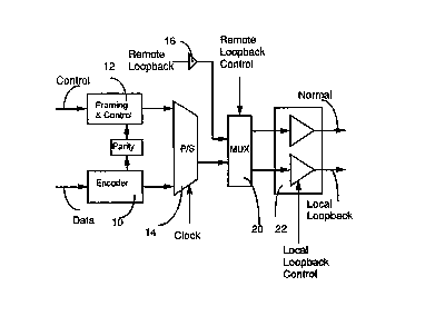
respective semiconductor chip. Therefore in Figure 1, there are
illustrated an encoder 10 and a framing and control circuit 12, both of
~; ;15 which are connected to a ~serializer 14. The encoder 10 receives a parallel
data signal and sends an ~co~le~l data signal to the serializer 14. At the
same time, a parity check signal is sent to the framing and control circuit
;~ ~12. The framing and control circuit 12 includes a frame pattern
generator which~generates frame bits in a distinct frame pattern. The
20 ~ circuit obhins control ~si~n~ls and mixes them with the generated frame
bits. The mixed frame bits and control s~ are sent to the serializer
14 which converts to a serial bit stream. A multiplexer 20 multiplexes
various serial bit streams and a driver circuit 22 transmits multiplexed
serial bit streams to a~receiver. The driver circuit 22 includes amplifiers
2s for a normal output and loopback output, the latter of which is used for
system testing of the comnlllnic~tion pat~s. The transmitter also
indudes a remote loopback circuit 16 to h~n-lle a remote loopback input
;for testing.
Figure 2 shows a receiver in brief diagrams. The serial bit
30 streams, normal input and loopback input, from the transmitter are
received and processed at a line driYer 24. After having been
demultiplexed at a demultiplexer 28, a bit stream is converted to a
I~ , * ~ ~
~ ~ ' $ ! ~ I ''7' i
WO~2/22l60 2~ D ~ 4 2 ~ Pcr/cAs2/oo22o
, u
parallel signal at a deserializer 30. The deserializer 30 separates frame
and control bits and data bits, both of which are respectively sent to a
:,
framing and control circuit 34 and a decoder 36. A loopback means 38
produces loopback conkol signals. An error signal is produced at a
parity check circuit which compares signals from the framing and
control circuit and the decoder. A remote loopback circuit 32 handles a
remote loopback output for testing.
Figures 3 and 4 show a flow chart and a circuit diagram,
; respectively, of the encoder illustrated in Figure 1. It should~be noted
0 that the following description deals mainly with a specific embodiment
of a line coding scheme of the present invention. The embodiment
finds its applications chiefly in high speed telecommunication.
However, simil~r or same line coding schemes can be used in various
areas of data comnl-mications.
The important criteria for a code to be used in high speed
telecommunication are:
- data tranTarency;
- control codes;
robust ~ framing, not requiring a synchronization
sequencei
; - bounded dc balance to permit ac coupling;
- bounded run length and high kansition density for clock
, ;~ recov~ly; and
- two level code.
In one of the preferred embo~ ents which will be
described below, the code is based on 20 bit long blocks. The coding does
not carry a~oss blo:ck boundaries (except to maintain dc bal~nce). The 20
bits are ~-~si~ne~ in the following manner:
- 17 data bits (B~B16)
- 1 bit for increasing transitions (T~
- 1 bit for ensuring dc balance (D)
- 1 bit for framing and control codes (F).
wo 92t22160 21 ~ 9 4 2 8 Pcr/cA92/oo22o
The description below follows the flow chart of Figure 3.
The steps described are not always carried out exdusively at the boxes
indicated but may involve other boxes numbered or unnumbered.
, ,
s Step 1 ~at box 40): Apply inversion to bits B3, B6, B7, B9, B11, B12, B13,
B14, B16. This step is included to distribute the energy in the data
spectrum for a static pattern of all zero data or all ones data, and thus to
reduce EMI (Electro-Magnetic In~elfer~llce). There exists a input pattern
that will produce a square wave line pattern, however it is unli~ely to be
lO maintained for any significant length of time. This step can be
eliminated for a circumstance where EMI is not a problem or other bits
. .
may be selected for inversion for other circumstances.
i~ :
Step 2 (at box 42): A transition bit set to zero (T=0) is added to the B16
15 side of the block. The block is checked to determine how many bits are
zero. If nine or more are zero, then all bits are inverted. Thus the
transition bit is set if the inversion took place, and is ~ero otherwise.
Output [B0', B1',...,B16', Tl
:
20 Step 3 (at box 44): The 18 bits are converted into Non-Return-to-Zero-
In~ert-on-Ones ~ l). This operation turns the ones ob~ained in the
previous step into transitions. This operation begins at T and proceeds
across to B0'. The level prece~1in~ T is assumed to have been a zero
(thefe~ore T=T") Output: lB0", B1",...,B16", T"]
Step 4 ~at box 46): A dc balance bit set to zero (D=0) is added to the T bit
side of the block. The block balance of the resulting 19 bit code is
calculated (number of ones - number of zeros). Output: ~B0",
B1 ",...,BI 6",T",D]
Step 5 (at box 48): The dc block balance is compared to the accumulated
system balance. The bits are inverted if the signs are the same. The
wo 92/22160 2 1 i3 ~ '12 ~ Pcr/cA~2/oo22o
~ g
,;~
, purpose of this operation is to reduce the absolute value of the
accumulated balance. It should be noted that the balance of the block can
~,~; never be zero, but ~he system balance can. When this is the case, blocks
with a positive balance are inverted at box 50, and those with a negative
- 5 ba}ance are not. After this operation, the D bit is set if an inversion
occurred, and is ~ero otherwise. Output ~B0~, B1't,...,B16~,T~,D]
.,
Step 6 (at boxes 52): The calculated dc balance is added to the
accumulated system balance if no inversion occurred and subt~acted if it
0 did (algebraic su~nation). (The system b~l~nce is set to zero on power
up or reset.)
. .
Step 7 ( at box 54): The frame bit is added to the D bit side of the block.
The framing sequence ls produced by a recursive 4 bit shift register,
5 which will be shown below. This produces a sequence which is 15 bits
long. Three of these lS bits are reserved to carry control information.
These three bits are id~tifiell by dec~ding 3 unique states of the shift
r egister. Output [B0*, B1*,...,B16~,T*,D,F]
' ~ ~ 20 Step 8: The block is transmitted serially. The F bit is transmitted ~irst
and B0 last. It should be noted that the effect of the F bit on the dc
bAlonce is ignored.
~;; py~mple:
~ ~ System dc R~1AnCe = 6
,
25 Next frame bit = 1
Input 17 ~ata bits 001100û0011111010
Step 1 00100011001000111 SelectiYe inversion
Step 2 110111001101110001 Inversion
Step 3 101101000100101111
Step 4 1011010001001011110 Add D=0 (Block Balance = 1)
Step S 0100101110110100001 Inversion
Step 6 System R~l~nce = 5
Step 7 01001011101101000011 Add F=1 or 0
WO 92/22160 , ~ P~CA92/00220
~;l 21 G~42~
,,, 10
Figure 4 is a block diagram of the encoder, and further
includes the complexity which indicates the amount of hardware which
may be required to accomplish these functions. The complexity shown
is a set of estimated values and the actual figures may vary not only in
5 numbers but breakdowns of stages.
As in Figures 3 and 4, the decoder f1lnctions are illustrated
in Figures 5 and 6 as a flow chart and a circuit diagram respectively. The
description below follows the flow chart of Figure 5. The incoming
,
' serial stream is [BO~j B1~,.. ,B16~,T~, D, F].
.',. 10
,
Step 1 (at box 60): Align to frame and remove frame bit. Output: [B0~,
B1 ~,. . .,B16~,T~,D]
~- ~ Step 2 ~at box 62): Invert if D-1 and remove D bit. Output: [B0",
.
' ~ 15 Bl",.. ,B16",T"]
,,
Step 3 (at box 643: Reverse ~e NRZI. Output: lB0', B1',...,B16',T'}
;'~ : '-
c ~ ~ Step 4 (at box 66): ~ Invert if T=1 and remove T bit. Output: lB0, B1,.. ,B16]
20 ~16 data bits and 1 cell frame pulse bit)
Step S (at box 68): Apply selective inversion to bits (B3, B6, B7, B9, B11,
B12, B13, B14, B16)
~:;
2s Step6: Outputparalleldata.
Example:
; ~ System dc p~ nce = 6
Incoming serial bits 01001011101101000011
Step 1 0100101110110100001
i ~ 30 Step 2 101101000100101111
. Step3 110111001101110001
'~ ~ Step4 0010001100100û111
Step 5 00110000011111010
:
~,~
,
J.
WO92/22l60 2 ~ ~ ~J 12 8 Pcr/cAs2/oo22o
," 11
Figure 6 includes a block diagram of the decoder and the
complexity.
The ~rame pattern is a self synchronizing pseudo-random
pattern of length 15. Three of the bits will be overwritten to carry
5 control codes. The frame pattern creation circuit is shown in Figure 7.
In the figure, a set of four shift registers E0, E1, E2 and E3 are used to
; generate the pseudo-random bit pattern for framing. There is also
shown in the figure a control bit insertion circuit 72 which receives
three control logic bits C1, C2, C3 for modifying bits in predetermined
0 positions w~thin the framing pattern. In this embodiment, the control
logic bits are used for the control of certain functions in the data
communication, such as equipment testings ~loopback testings) in
addition to the no~nal mission. The pseudo-random pattern of 15 bits
long generated by four shift registers is shown in Flgure 8.
5 ~Three control logic bit positions occur when E2 and E0 of
the shift register are zero. The rem~inin~ two bits determine which
control bit is indicated. If all ~e bits are zero, a one is shifted into E3 of
the shift register to kickstart the framing sequence. Thus:
,
~ ~ ~ State ~ E3 E2 E1 E0
O O 1 0 Control Logic Bit
0 0 0 Control Logic Bit
0 1 0 Co~trol Logic Bit
25 ~ ~ Kick Start 0 0 0 0 ~lsallowed State
A control logic bit is asserted by inverting the frame bit that
would normally occur in that position. Control logic bits are not acted
upon ~ntil framing is establi~e-1. A s~:robe signal will be pro~ided to
30 in~ te when the externally accessed con~ol logic bits may be changed.
It will occur when 1111 is held in ~e shift register.
In the present embo~liment, combinations of C1 and C2 are
used for mission for transmitting data, and for testing the system by
wo 92/22160 Pcr/cA92/00220
~1 09'1~8
12
looping back test data through the transmitter or receiver. C3 is
dedicated to link error monitoring.
The four possible combinations Qf C1 and C2 ar~ assigned
in the following table
C~ C1 Control Code
O Mission (Normal Mode)
0 1 ~ission (Normal Mode)
0 1 0 RepeaterLoopbackControl Code
Remote Loopback Control Code
.
In the mission mode the parallel data is encoded, the
frame and control logic bits are added, and then converted to serial
format using an internally generated clock. The loopback modes are
used ~or system testing of the communication paths. In local loopback
mode the serial data is~sent through the local mate receiver to test its
functionality. The remote loopback mode tests the serial tran~lnicsion
mediurn used in a bidlrecfion~l link.
Figure 9 depicts~a configuration of a bi-directional link
:
using pairs of transmitters and receivers. A transmitter Tx1 and receiver
are a; local set located at one location, and a transmitter Tx2 and
eceiver Rxl are a remote;~set~ located at another loc~tion~ Serial data bits
and other control or frame bits ~are sent in direc~ions shown therein. A
25~ selection of contro 1 signals~ determines the mode of operations and
selecfs the proper paths~for such~operations. Figure 10 on the other hand
i llustrates a configuration~ of a bi-directional link using pairs of
-
transmitters and receivers in ~ition to repeaters.
~ Referring back to Figure 7, the control logic ~it ~3 in the
.
30 framing sequence ca~ries a parity bit that covers the data after encoding
(before decoding). It does not cover the frame bit. As the parity is
inserted only ~nce in a frame it covers 19~15 bits. The control logic bit
strobe signal is used to update the parity value.
WO 92J22160 2 ~ ?, 8 Pcr/cA~2/oo22o
13
The frame bit in the code according to the present
invention does not interact with the rest of the block This allows
greater freedom in choosing the frame pattern and also the line interface
part of the system design re~nAirls completely independent of data
5 structure. Any frame length or pattern can be chosen to fit the needs of
the con~ nirAtion syslen-. Also, in the case where the data has been
previously encoded with;fr~m;n~, by choosing a frame length that is not
a fraction of the previous frames, the possibility of r~imil king the frame
pattern by static data is virtually eliminated This method has allowed
10 the use of a circuit which generates'effi.~ient pseudo-random codes for
frAming patterns.
The length of the frame pattern and the framing state
m.~hine combine to define the average reframe and false frame times
and the probability of static data imihtin~ the frame patle~n By using a
15 two-state frAminf~ algorithm, the time to loss of frame due to random
errors can be si~nific~ntly increased. This algorithm requires two
coI~ce~ .ve frame words to have errors~before a frame is coIlc;~1ered lost
It also requires two consecutive corréct ~frame words before a frame is
;~; found. This has negligible~ effect on the l~fralne time.
2 0 Using ~ this~ algorithm the ~ reframe time (based on average
n~intenAtlce time~for hlse~frame);is less than 1~1 second for frame
yall~u length from~4~to 32~bits~ At the shortest~frame pattern the time is
donninated by fa~lse~fr~min~,:at'~e longest;by~the time taken to load the
patteM. ~ The mainPn~nce time~ass~ing a~ bit error rate of 10-14 iS
25 essentîAlly forever ~Thus,~within the'~range of 4 to 32 bits the *ame
' length is not critical, ~
While Figures~ and 2~ ' show encoding and decoding
operations on parallel~data;~streams at the block rate, it is of course
possible to perform~such~operat}ons on-serial data streams at the
- 30 transmission rate. Therefore as shown in Figure 11, a transmitter
includes a parallel-to-serial~ converter which is located ahead of an
encoder for the serial ~opera~tions. A combiner combines the frame and
WO g2/22160 Pcr/cAs2/oo22o
21~42~ 14
encoded serial bits. A receiver can be arranged in a similar fashion for
reverse operations.
The properties of the coding scheme according to the
present invention have been analyzed by a combh~ation of analytical
5 methods, exhaustive code combinations, and random data simulations.
The last two methods involved computer analysis due to the number of
possible data combinations in 17 bits of data (131x103). The resulting
statistics on the run bound and the dc bAl~nce appear below.
Comparisons are made with the HP (Hewlet-PackardTM)
10 code and the FDDI 4B5B code. These codes are the most simil~r to the
code according to the present invention. The HP code is made up of
four blocks of 4BSB and can be collci~ored~as 16B20B or modified 4B5B.
The HP code is ~e~crihe l in detail in the Procee~lin~ of the 1989 Bipolar
Circuits and Technology MeetinE on ~.,~l~mber l8-19, 1989, in an article
5 entit1e~1 "A ~'hipset for Gigabit Rate~ Data Co~nntunication" by Walker et
al, pp. 2B8-290.
Overhead
Of the 20~bits in ~a~code block, ~ere~ are 3 bits of overhead
20 ~which provide imyro~v~ ent in~the tr~nC~i~sion characteristics, control
codes and framing~for~the link. This~ co~ ds to 15% overhead. The
;; HP code uses 4 Wts~ out of a 20 bit block to provide these features (20%
overhe~ l). T~e 4B5B~encQ~ uses 20% overhead to provide the data
tr~nc~icsi~l chara~l~;slics.~ Additional~bandwidth would be nee-1e~ to
25 provide framing~and control codes. ;~
,
Tr~n~itin 1 D~,~silx and Run Bound~
The ~code ~ accordmg to the present invention has a
mininlum of ~ 9 tr~nciHons in eac~ 20~ bit block. This gives a minimum
; ~30 transition-densiq~of 44%~and a maximum run bound of 19. This run
; ~bound can only occur acrass block boundaries. It occurs very
infrequently and is~ separated~by at least 18 transitions.
::
wo 92/22160 ~ 2 g PCI'/CA92/00220
The HP code has a minimum transition density of S%, as
only one transition is guaranteed in the 20 bit bloclc. The run is 20 bits.
This occurs only within a block, but can occur in adjacent blocks as many
times as the data remains unchanged. The 4B5B has a minimum
5 trAnC;tiQn density of 40% and a run bound of 3 bits.
DC Balance
The accumulated dc imbalance cannot exceed +8, -9 bits
using the code of the present invention (measured at block boundaries
lo and not including the frame bit). Within blocks the im~ nce can reach
+13 or -14 bits. The HP code bounds the dc imbAl~n~e to i19 bits at block
boundaries, and +~8 within block. In 4B5B code, each ~ode has a b~1Ance
of +10%. Th~l~erore, the code can have a dc drift of up to ilO% at all
freq -enries.
15In an ac coupled s~ystel 4 dc inlbA1~nce in the transmitted
; signal causes the mid height of the received pulses to be shifted from set
sampbng point. This causes~eye closure. ~
In a code (like the code;ac,J~i..g to the y.ese.-t inven'~ion)
where~both s)~sle.n dc inlbAl~nce and run length are bo11n~1e~, the longer
20 of ~ the two bounds determines the maximum eye closure due to ac
coup~g. ~ Thus, in ~this code, it is ~1~termir~ed by the run bound of 20 bits
(Induded~ frAmin~
%Droop = R(T)(100)~ ~ ~
where: R = Run bound (20 bits)
T = bit period~ (1 ns)
=; time conslant of ac coupling filter (RC)
30 Circl~it Complexity
Comparisons of clrcuit complexity are difficult to make
meaningful unless the~ same amount of time is spent optîmizing each
implementation. Thc HP code can be reasonably estimated as requiring
::
:: ~
WO 92/22160 PCI /CA92/00220
16
2/3 the circuitry as the code of the present invention as the HP code only
pe.~l.ns 2/3 the operations on the data.
Even ~ough the present code requires more circuitry than
the HP code, it is not e~cessjve. A rough estimate in terms of equivalent
s 2 input gate is 1.6k gates for the encoder, and lk gates for the decoder.
These estimates include the framing circuitry, control circuitry and
retiming flip-flops. For co~ ,arison purposes, the alignment buffer in
the receiver is estimated at 2k gates.
0 ErrorMultiplication
If one~ bit in this code is corrupted in transport, several bit
errors may result after ~lecodingt These errors never span across 16 bit
words. Thus, if the data is used on a word basis, the error multiplication
effect is important only ~ln the manner in which error detection is
5 encoded into the data itself. I t should be noted that parity on a word
basis~is a particularly poor~choice as it will miss the majority of single bit
errors.
The following table shows the result;to the output data of
each possible single bit~error:
20 ~
Bit in Error ~ Result
:
F~ No ~errors in output data~ will cause
change in Frame or Control Code state
~ machine
B~ lipsall~bitsexcept B16
Bl-Bl6 ' ~ Errors in bits Bn and Bn-l
, B0 ~ ~ Errors in bit B0
::