Note: Descriptions are shown in the official language in which they were submitted.
CA9-93-021 1 2109682
MULTIPLE BUS INTERFACE
Field of the Invention
The present invention relates to personal computers
and more particularly to the implementation of adapter
cards that can be used to connect to computers with
different bus architectures with a single bus of a desired
architecture.
Backqround of the Invention
The IBM~ personal computer family was established as
a standard which has been adopted by thousands of computer
companies. Following from the inception of the first
personal computer which used to PC bus, the personal
computer AT was subsequently introduced by IBM and used a
slightly different architecture called the AT architecture.
This architecture has been used in the IBM Personal
Computer AT, the IBM Personal Computer model 25, and 30,
and other IBM computers and the personal computers produced
by many companies worldwide.The AT bus has been accepted as
the ISA standard for personal computers. Subsequent to the
introduction of the AT, architecture IBM introduced the
microchannel architecture, or the Micro Channel Bus as it
is normally called. This bus was used in the IBM PS/2
Models 50,55,60,70,80,90,95, among others and in computers
made by other companies. Subsequent to the development
architecture, advances were made in miniaturization of
electronic circuits and memory such that it became possible
to store tremendous amounts of data in a small format and
the PCMCIA architecture was born. Other architectures have
been developed such as the EISA architecture, the PCI
Architecture and the VESA architecture. Different
architectures have evolved in response to the evolution of
computer microprocessor capabilities.
To provide flexibility in the design of accessory
boards for different bus architecture it would be desirable
if a single integrated circuit could accommodate any of
these bus architectures so that for instance an Infrared
communications adaptor could be constructed for an AT, MCA
or PCMCIA bus using the same integrated circuit. This
would reduce the need for the development for ICs for each
~_ 2109682
CA9-93-021 2
bus.
No references have been found by the applicant which
disclose a multi-bus interface adapter that can permit one
IC to be used in manufacturing the same product for several
different bus architectures.
Summary of the Invention
The present invention provides a circuit, for instance
a module or integrated circuit, that can be used to connect
systems with different architectures to a common expansion
option.
Basically this invention provides a circuit which
transforms signals conveyed on any of a number of
architectural busses into a standardized bus protocol to be
used locally on an adapter card or module to provide a bus
connection for a functional device, such as a diplay driver
on the adapter card.
One aspect of the invention provides a multiple bus
interface adapter, or module for connection to the bus of
a data processing device. The adapter includes a common
interface or group of lines for connection to any of
several bus architectures for operation therewith. The
interface adapter includes:
(a) a control interface for accepting control signals
from the bus of the data processing device,
(b) an address interface for accepting address signals
from the data processing device, and
(c) a data interface for accepting data signals from
said data processing device.
A bus identifier is provided for identifying the bus
architecture of the data processing device, as well as a
bus protocol decoder responsive to the bus identifer.
The decoder derives its input from the control
interface, and is adapted to produce as an output
standardized local control signals derived from the data
processing bus control signals for use by a local
functional device to be accessed by the data processing
device.
The interface can be bidirectional depending on
architectural and functional requirements.
The bus protocol decoder advantageously can be
2109682
CA9-93-021 3
responsive to the bus identifier to derive protocol
specific control signals from control signals from the
control interface.
Also, address capture logic coupled to the address
interface using transparent latches enabled by control
signals from the control interface can be used to provide
a standardized local address for the local functional
device.
In addition, local functional enable logic responsive
to the standardized local address can provide an activation
signal to the local functional device.
The local functional enable logic can provide feedback
to the data processing device.
The feedback can include acknowledgment of receipt of
the standardized local address and a corresponding
standardized local control signal.
The acknowledgment (signal) can include an
acknowledgment signal from the local functional device
signifying completion of the function initiated by the
standardized local control and address signals.
The bus identifier can convey bus identification to
the local functional device.
Brief Description of the Drawings
A better understanding of the present invention can be
had by reference to the following detailed description of
an embodiment of the invention in conjunction with the
following drawings in which;
Figure 1 is a representation of an overall system
diagram.
Figure 2 is a representation of bus protocol decoder
logic.
Figure 3 is a representation of common input receive
circuitry.
Figure 4 is a representation of system address capture
logic.
Figure 5 is a representation of data routing logic.
Figure 6 is a representation of mode selection logic
(bus identifier).
Figure 7 is a representation system access detect
logic (local functional enable logic).
~, 2109682
CA9-93-021 4
Detailed Description of a Preferred Embodiments of the
Invention
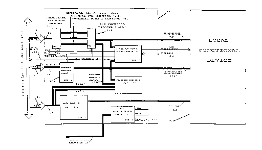
Referring to Figure 1, it can be seen that the
embodiment of the invention, adapter 1 illustrated is
composed of interface lines (2), (3), (4) for connection to
a computer system bus (5) consisting of Control (6),
Address (7) and Data (8) portions. The adapter (1) is
intended as an interface from a computer system to a local
functional device (9) the adapter provides a local bus
consisting of Local Control (10), Local Address (11) and
Local Data buses (12), which connect to a Local Functional
device (9).
The adapter (1) can be seen to be further composed of
Common Control Input Receive Circuitry (13), Bus Protocol
Decoder Logic (14), Local Functional Enable Logic (15),
Address Capture Logic (16), Data Routing Logic (17),
Platform Specific Logic (18) and Bus Identifier Logic (19).
The current embodiment of the invention is designed to
conform to any one of ISA, Microchannel or PCMCIA bus
specifications. The embodiment illustrated is an
implementation of a Memory and I/0 Slave to the computer
system to which it is connected. Accesses to the adapter
(1) are passed to the local functional device (9). Those
skilled in the art will recognize that support for more
comprehensive use of system capabilities (such as DMA and
interrupts) would be possible by extension of the
principles defined herein.
A summary of the operation of the current invention is
as follows. When bus cycles are executed on the computer
system bus, the adapter (1~ determines the validity of the
current bus cycle as it pertains to the local function
being supported. This involves for one thing decoding the
input control signals to determine the cycle type being
performed, for example memory read, memory write, I/0 read
or I/0 write. In the case of memory accesses, any
necessary decode of the System Address (7) is done to
determine if the address range being accessed by the system
is in the range allocated to the local functional device
(9). In the case of input/output (I/0) accesses, the
adapter circuitry decodes the system address to determine
if the I/0 port being accessed is allocated to the local
2109682
CA9-93-021 5
functional device. When a valid address is detected on the
System Address while a valid cycle type is detected, the
adapter (1) will activate the CYCLE_ACTIVE signal on cycle
active line (20) to the local functional device (9)
accompanied by the standardized local control signals on
local control bus (10) and the standardized local address
on local address bus (11). The adapter (1) will also
generate the necessary feedback signals to the computer
host system as required by the specific system bus being
interfaced to. One important such feedback signal is the
CYCLE_EXTEND signal on line (21) (in ISA and Microchannel
this is IOCHRDY and in PCMCIA this is WAIT-) which is used
by the adapter (1) to extend system bus cycles until the
local functional device (9) has completed the requested
operation or transaction (indicates by a CYCLE_END signal
on CYCLE_END line (51) generated by the local function).
It will be clear to those skilled in the art, that the
function of the CYCLE_END signal would not be necessary in
the event that the Local Functional device (9) is a zero
wait state device on all platforms (in other words capable
of meeting the fastest system cycle times). In the event
however that the local functional device (9) may require
variable time to respond to system accesses (for example in
the event of a local function that implements a form of
local direct memory access or DMA) the CYCLE_END signal is
used by the local functional device (9) to indicate when it
is ready for the current system cycle to terminate and
hence complete the operation. Consider a system access
initiated while the local function was performing a local
Direct Memory Access (DMA) operation, for example, the
completion of the system cycle would have to be delayed
until the local DMA operation had completed and the local
resources could be granted to the host for the pending
cycle.
As much as the current embodiment strives to unify the
interface to the three system busses, when there are
platform specific requirements to be met to maintain
specification compliance, then platform specific logic, eg.
logic (18) will be necessary.
For example, the Microchannel architecture specifies
the use of Programmable Option Select (POS) Registers for
2109682
CA9-93-021 6
expansion card resource allocation, (eg. memory or I/0
address ranges) which those skilled in the art of
Microchannel adapter design will be familiar with both in
their implementation and application.
In the ISA architecture, resource allocation is
typically performed by on board DIP switches which connect
to an ISA interface as is the case in the present
embodiment. Those skilled in the art of ISA Adapter design
will be familiar with variations of this technique and will
be familiar with their application.
In the PCMCIA architecture, Attribute memory is in a
unique and mandatory memory space (if PCMCIA specification
compliance is desired) used to control resource allocation
and some generic PCMCIA functions. Those familiar with the
PCMCIA Architecture will be familiar with implementations
and applications of the PCMCIA Configuration Registers and
the Card Information Structure (CIS) of Attribute Memory.
With reference to Figure 3, it can be seen how common
control input receive circuitry (13) which receives host
control signals via input pins (or bus lines) 2 (Input 1,
Input 2, Input 3, Input 4, Input 5 and Input 6) is used to
generate three sets of signals, namely, Internal ISA
Control (22), Internal MCA Control (23) and Internal PCMCIA
Control (24).
With reference to Figure 2, the Bus Protocol Decoder
Logic (14) is seen taking Internal PCMCIA Control (24),
Internal ISA Control (22) and Internal MCA Control (23) as
its inputs and producing Standardized Local Control (10)
and Platform Specific Control (25) as its outputs. The Bus
Protocol Decoder Logic can be seen as comprising PCMCIA Bus
Protocol Decoder Logic (26), MCA Bus Protocol Decoder Logic
(28), ISA Bus Protocol Decoder Logic (27) and a Protocol
Decoder Funnel (29).
The ISA Bus Protocol Decoder Logic (27) uses Internal
ISA control (22) as inputs and produce output on lines
(31). Figure 2a illustrates the details of the ISA Bus
Protocol Decoder Logic (27).
With further reference to Figure 2, the MCA Bus
Protocol Decoder Logic (28) can be seen to take input on
lines (23) and produce output on lines (32) and (25b).
Figure 2b illustrates the details of (32) and (25b) as
2109682
CA9-93-021 7
outputs. Figure 2b illustrates the details of the MCA Bus
Protocol Decoder Logic (28).
With further reference to Figure 2, the PCMCIA Bus
Protocol Decoder Logic (26) can be seen use lines (24) as
inputs and produce outputs on lines (30) and (25a). Figure
2c illustrates the details of the PCMCIA Bus Protocol
Decoder Logic (26).
With further reference to Figure 2, the Protocol
Decoder Funnel (29) can be seen to use lines 30, 31 and 32
as inputs and produce outputs on the Standardized Local
Control line (10). Figure 2d illustrates the details of
the Protocol Decoder Funnel.
Again referring to Figure 2, the Platform Specific
Control Lines (25) can be seen to be the combination of the
PCMCIA Protocol Decoder Platform Specific Lines (25a) and
the MCA Protocol Decoder Platform Specific Lines (25b).
The functioning of the bus protocol decoders will be
readily apparent to those familiar with ISA, MCA and PCMCIA
bus architectures.
With reference to Figure 2a, the generation by ISA
protocol decoder (27) of ISA output ISA protocol decoder
signals ISA_READ, ISA_WRITE, ISA_IORD and ISA_IOWR are
mutually exclusive by the specification of the ISA bus in
that only one of MEMRD-, MEMWR-, IORD- or IOWR- will be
active during a slave cycle. One of these four output
signals will be asserted during ISA slave memory read/write
operations and slave I/O read/write operations.
Referring to Figure 2d; in the event that one of these
ISA output signals become active, a local control signal
(LOCAL_READ-, LOCAL_WRITE-, LOCAL_IORD- or LOCAL_IOWR-)
will be generated by the protocol decoder funnel (29) on
local control line 10 at the output of the corresponding
three input NOR gate. It should be noted that for
activation, for a ISA output on bus (31) input bus ISA must
be high indicating adapter (1) is in ISA mode of operation
as a result of input from bus identification logic (19).
In the event that ISA line 33 is low, the four signals
ISA_READ, ISA_WRITE, ISA_IORD and ISA_IOWR will be inactive
or low hence not able to activate any of LOC_READ-,
LOC_WRITE-, LOC_IORD- and LOC_IOWR-.
In Figures 2c and 2d are depicted the corresponding
2109682
CA9-93-021 8
PCMCIA protocol decoder (26) and Microchannel protocol
decoder 28. As was the case with the ISA protocol decoder
~27~, the assertion of any of the MCA decoder output (32)
signals or PCMCIA output decoder (30) signals requires the
corresponding mode signals MCA or PCMCIA from the bus
identifier logic (19) to be active respectively. It should
also be noted that the Microchannel protocol decoder (28)
produces two specific signals, MCA_SETUP_WR (25(b(1))) and
MCA_SETUP_RD (25(b(2))) which will only be generated during
system configuration operations in a Microchannel system
while accessing Programmable Option Select (POS) registers
which would be implemented in the platform specific logic
18 (not illustrated). Likewise, the PCMCIA protocol
decoder (26) produces two specific signals, ATTR_RD
(25(a(2))) and ATTR_WR (25(a(1))) which~ are generated
during system accesses to PCMCIA Attribute memory space.
These platform specific control signals (25(1(1)),
25(a(2)), 25(b(1)), 25(b(2))) are used by the Platform
Specific Control logic (18) in the current embodiment. For
both the Microchannel protocol decoder (28) and the PCMCIA
protocol decoder (26), all of the outputs are mutually
exclusive, meaning that only one output can be logically
active at the same time.
With reference to Figure 4 showing the address capture
logic (16), the system address produced by the various
system busses are captured differently.
PCMCIA addresses are held stable by a computer which
uses PCMCIA architecture during each transaction and hence
need not be latched internally.
A 16 bit ISA bus uses 24 bit addresses (System
Addresses 0-23).
System addresses 0-19 (SA[l9:Ol) are provided across
a standard 8-bit ISA connector (not shown) and are stable
throughout system accesses. ISA system addresses 20-23
(LA[23:20]) are not stable and must be latched locally by
the System to Local Interface adapter (1).
Microchannel architecture uses system addresses 0-23
([23:0]) all of which are not stable and must be latched by
the System to Local Interface adapter (1).
ISA addresses are latched using the ISA bus signal
BALE (22a) (Bus Address Latch Enable), and Microchannel
~, 2109582
CA9-93-021 9
addresses are latched by the MCA bus signal ADL- (23a)
(Address Latch). The active signal (BALE or ADL-) and the
proper level are selected by the address capture logic (16)
based on the state of the MCA output from bus
identification logic (19) according to the architecture
being interfaced to (ISA (uses BALE) or MCA (uses ADL-)).
The Address Capture Logic (19) also selects which address
to use, the unlatched addresses SA[23:0] for PCMCIA, the
latched address SA_L[23:0] for MCA or the combination
address (latched SA_L[23:20], unlatched SA[19:0]) for ISA
to generate ADDR[23:0~ which may be driven as required by
the local functional device (9) onto the Local Address bus
11 to the local functional device (9).
With reference to Figure 5, it can be observed that
the data routing logic (17) connects system to local data
through input buffer (36) and local data output driver tri-
state buffer (38); and local data to system transfer using
local data input buffer (39) through tristate buffer (40)
through system data output driver tristate buffer (37). The
process of transferring data to or from the system bus (5)
is as follows: System data is received at the System Data
pins (2) of the adapter (1) and is routed through the Data
Routing Logic (17) to the Local Data bus (12) in the case
of a write operation, or Local data is received at the
Local Data lines (12) of the adapter (1) and is routed
through the Data Routing Logic (17) and driven onto the
System Data bus (5) in the case of a read operation.
Platform specific operations occur independently of the
Local Data Bus (12) and data may be exchanged with the
system bus 5.
Data can be sent to the platform specific logic (18)
through system data input buffer (36). Data can be
transferred from platform specific logic (18) to the system
data bus (8) through tristate buffer (41) and system data
output driver tristate buffer (37).
Tke tristate drivers (37), and (40) are enabled by
system reads of data from the local data bus (12).
Drivers (37), and (40) are enabled during system reads
of platform specific data.
Driver (38) is enabled on system writes to the local
data bus.
~_, 2109682
CA9-93-021 10
Figure 6 illustrates the bus identification logic (19)
which uses the input condition to mode pins (42) to
generate the ISA, MCA and PCMCIA signals used throughout
the adapter (1). It can be seen that these signals are
mutually exclusive in that only one can be high at any
point in time.
Figure 7 illustrates the decode that is performed on
the local control signals (LOC_READ-, LOC_WRITE-, LOC_IORD-
and LOC_IOWR-) on local control bus (10) in conjunction
with the captured address (ADDR[23:0]) to detect the
occurrence of a valid system cycle and to generate the
corresponding CYCLE_EXTEND and CYCLE_ACTIVE signals. The
Captured System Address ~ADDR[23:07]) is compared to the
supported address ranges for Memory and I/O in both ISA and
Microchannel architectures. The difference between the two
is the source of the supported address range. In the case
of operation in ISA mode, the settings of external switches
(ISA_SWITCH 52 Bus on Figure 7) may be used to position an
window (eg. 8 kilobytes) of accessible local memory in the
system address range HEX COOOO-HEX DFFFF (commonly referred
to as the C and D segments) on one of 16 possible 8k
boundaries in that range; ie: HEX COOOO, HEX C2000, HEX
C4000... where a hexadecimal increment of HEX 2000 e~uates
to an 8k step in memory space. The same operation is
performed in the Microchannel architecture except that the
allocated address range is determined according to the
contents of MCA_POS (53), the Programmable Option Select
(POS) registers in the Platform Specific Logic (18). In
the current embodiment, this address range positions an
8kilobyte window on one of 16 possible 8k boundaries in the
C and D segments.
In PCMCIA architecture, this address validation
operation is not required. In the case of I/O accesses,
the same approach is used as above to determine if the
System Address being presented falls within the active 16
byte block of I/O space. The active block of I/O space in
the current embodiment is one of 8 16-byte boundaries in
the range HEX 300, HEX 310, HEX 320, HEX 330, HEX 340, HEX
350, HEX 360 or HEX 370. Again, the active setting is
determined in ISA by DIP switch settings (eg. external to
the Adapter (1)) and in Microchannel by the settings of
2109682
CA9-93-021 11
Programmable Option Select registers. The CYCLE_ACTIVE
signal is active as long as a valid system cycle condition
is detected. The CYCLE_EXTEND signal is asserted as
feedback to the system in the presence of CYCLE_ACTIVE and
the absence of CYCLE_END. Those skilled in the art will
observe that zero wait state operation of the interface is
capable by forcing the CYCLE_END signal to the active state
at all times and hence eliminating the assertion of
CYCLE_EXTEND to the system.
The Platform Specific Logic (18) indicated in Figure
1 and Figure 5 (the data routing logic) is used to support
platform specific requirements such as the implementation
of the Microchannel POS registers, PCMCIA Attribute Memory
and the current embodiments usage of external DIP switches
to determine the active system memory and I/O ranges in an
ISA system. The details of the implementation of the
Platform Specific Logic are not described as the contents
of this logic should conform to the respective bus
specifications which are known to those skilled in the art.
Access to the Platform Specific Logic (18) may be
controlled by the Platform Specific Control signals (25)
and a decode of the captured system address lines (11)
where necessary. The detailed implementation of Platform
Specific Logic (18) is dependent upon the sophistication
desired of the adapter's capabilities.
The invention herein is not limited to the specific
embodiment shown. Many modifications may be made without
departing from the spirit and scope of the invention.