Note: Descriptions are shown in the official language in which they were submitted.
7 5 3
PHN 14.269 1 28.01.1993
Circuit arrangement.
The invention relates to a circuit arrangement suitable for high-frequency
operation of a discharge lamp, provided with ~ -~
- input terminals for connection to a low-frequency supply volhge source, -- rectifying means coupled to the input terminats for rectifying a low-
S frequency supply voltage supplied by the low-frequency supply voltage source,
- a first branch comprising first capacitive means and coMected to the
rectifying means,
- a DC-AC converter coupled to the first capacitive means for generating
a high-frectuency current from a direct voltage present across the first capacitive means,
10 and
- a further branch of which a first end is coMected to a point of the DC-
AC converter at which a high-frequency volhge is present during la np operation and of
which a further end is coupled to the rectifying means.
Highfrequency operation of a discharge lamp in this coMection is
understood to mean operation at an operating frequency of approxi nately 10 kHz and
higher. A low-frequency supply voltage source is understood to mean, for example, a
substantiatly sinusoidat mains voltage with a frequency of, for example, S0 or 60 Hz.
Such a circuit arrangement is known from US 4,782,268. The known
circuit a~Tangement comprises a DC-AC converter consisting of a bridge circuit. The
further branch comprises both inductive and capacitive means and in addition twodiodes. A first end of the further branch is connected to a junction point of two
switching etements forming part of the bridge circuit. A fur~her end of the further
25 branch is connected to an output of the rectifying means. It is achieved by means of the
further branch that the circuit arrangement behaves like an ohmic resistance to a
considerable degree during lamp operation. As a result, the circoit arrangement causes
only a comparatively small amount of interference in the low-frequency supply voltage
7 J ~
P~J 14.269 2 28.01.1993
source and a high power factor is realised by the circuit arrangement during lamp
operation.
- A disadvantage of the known circuit arrangement is that, in addition to the
diodes forming part of the rectifying means, further diodes are neressary, i.e. the two
5 diodes in the further branch, for realising the favourable properties of the circuit
arrangement as regards mains interference and power factor.
The invention has for its object inter alia to provide a circuit arrangement
10 for the high-frequency operation of a discharge lamp with which a comparatively high
power factor and only a comparatively small arnount of mains interference can berealised during lamp operation, while the means by which these favourable properties
are achieved comprise only a comparatively small number of components.
According to the invention, a circuit arrangement as described in the
15 opening paragraph is for this purpose characterized in that the further branch is
conductive for AC current in both diI~ections and the further end of the fur~er branch is
connected to a first input terminal.
In a circuit arrangement according to the invention, the further branch is
conductive for AC current in both directions (i.e. from the first end to the further end
20 and wce versa) and contaLns no diodes. Since the further end of the further branch is
coMected to an input terminal, the further branch couples a point of the DC-AC
converter at which a high-f~equency voltage is present during lamp operation to an input `~
of the rectifying means. It is achieved thereby that the diodes in the rectifying means
not only rectify the low-frequency supply voltage but also perform a function which
2S corresponds to that of the diodes in the further branch in the known circuit. As a result,
a circuit arrangement according to the invention has favourable properties as regards
interference in the supply voltage source and power factor, while the circuit
arrangement can at the same time be realised with a comparatively small number of
components. Thanks to this comparatively small number of components, the circuit30 arrangement is comparatively simple and therefore also comparatively easy to
manufacture.
An advantageous embodiment of a circuit arrangement according to the
invention is characterized in that the fur~er branch comprises second capacitive means.
"-
.
:: : -
-
.
~ l ;u ~ ~ ~ 3
PHN 14.269 3 28.01.1993
The capacitive means in the further branch prevent a direct current from flowingthrough the further branch. If these capacitive means were absent, a discharge lamp
operated by-means of the circuit arrangement might pass a direct current under certain
circumstances, whereby cataphoretic effects could occur in the lamp. When the further
S branch is connected to a further input terminal via third capacitive means in this
advantageous embodiment of a circuit arrangement according to the invention, thesecond capacitive means and the third capacitive means form a filter for suppressing
supply mains interference. The second capacitive means in such an embodiment of a
circuit arrangement according to the invention fulfil both the function of blocking direct
10 current and the function of filtering out interference in the supply voltage mains.
A further advantageous embodiment of a circuit a~Tangement according to
the invention is characterized in that the impedance of the further branch is substantially
zero. Since the further branch in a circuit arrangement according to the invention
contains no diodes, while it is not necessary in every embodiment to include second
15 capacitive means in the further branch, the further branch may be realised as a
conductive connection in this further advantageous embodiment, i.e. no components are
included in the said branch. As a result, this further advantageous embodiment of a
circuit arrangement according to the invention can be realised in a comparatively simple
manner and at a comparatively low price.
A further embodiment of a circuit aaangement according to the invention
is characterized in that the rectifying means comprise a voltage multiplier. When the
amplitude of the low-frequency supply voltage is comparatively low compared with the
operating voltage of a lamp operated with the circuit a~Iangement, it may be
advantageous to cause the DC voltage present across the first capacitive means in the
2S first branch to be comparatively high.
Embodiments of the invention will be e~cplained with reference to a
drawing.
In the drawing:
Fig. 1 shows an embodiment of a circuit arrangement according to the
invention;
Fig. 2 shows a further embodiment of a circuit arrangement according to
.... - . ...... , ~ ... .. . ~. . :
- - - -
.
-.
- .
. .. ' '' , ' .
~ ,~. .. ... :
PHN 14.269 4 ~ 7 ~ 3 28.01.1993
the invention; and
Fig. 3 shows an alternative embodiment of a circuit arrangement
according to the invention.
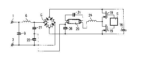
In Fig. 1, reference numberals 1 and 2 denote input terrninals for
connection to a low-frequency supply voltage source. The rectifying means are formed
by a diode bridge G. The first capacitive means and the first branch in this embodiment
are formed by capacitor 16. The DC-AC converter is formed by switching elements 18
10 and 19, control circuit S, coil 24, capacitor 31, and capaci~or 36. A discharge lamp 20
is connected to the DC-AC converter. The furtha branch, which in this embodimentcomprises capacitive means, is formed by capacitor 22. Capacitor 21 in this
embodiment forms third capacitive means.
Input terminals 1 and 2 are interconnected by capacitor 9. Input terminal 1
15 is also connected to a first end of coil 6. A further end of coil 6 is connected to input ~ -
terminal 2 ~rough a series arrangement of capacitor 21 and capacitor 22. The further
end of coil 6 is also connected to a further input of the diode bridge G, and input
terminal 2 is coMected to a further input of diode bridge G. A first output of the diode
bridge G is connected to a further output of the diode bridge G via capacitor 16.
20 Capacitor 16 is shunted by a series arrangement of the two switching elements 18 and
19. A control electrode of switching element 18 and a control electrode of switching
element 19 are connected to respective outputs of control circuit S. A junction point of
switching element 18 and switching element 19 is connected to a first end of coil 24. A
further end of coil 24 is connected to a first electrode of the discharge lamp 20. A -
25 further elestrode of the discharge lamp 20 is coMected to a first side of c~pacitor 36. A
further side of capacitor 36 is coMected to a side of capacitor 16. The discharge lamp
20 is shunted by capacitor 31. A junction point of the discharge lamp 20 and capacitor
36 in this embodiment forms the first end of the further branch. The further end of the
further branch is input terminal 2.
The operation of the circuit arrangement shown in Fig. 1 is as follows.
When the input terminals 1 and 2 are coMected to a supply voltage source
which supplies a low-frequency supply voltage, this low-frequency supply voltage is -
rectified by the diode bridge G, whereby a DC voltage appro~imately equal to the
.. . ..
- ~ ' - ' ' ' .
' ' :, . :. '. :' ' . :,
7 ~ ~)
PHN 14.269 5 28.01.1993 -
maximum amplitude of the low-frequency supply voltage is present across capacitor 16.
At the same time, the control circuit S renders the two switching elements alternately
conducting and non-conducting with high frequency. As a result of this, a high-
frequency current flows through the branch formed by coil 24, discharge lamp 20,5 capacitor 31 and capacitor 36, and a high-frequency voltage is present at a common
junction point of capacitor 36 and discharge larnp 20. The fact that this commonjunction point is connected to input terminal 2 through the further branch formed by
capacitor 22 achieves that the low-frequency supply voltage source supplies current
during time intervals in which the instantaneous amplitude of the low-frequency supply
10 voltage is lower than the voltage across the capacitor 16. This means that the amount of
interference (conducted interference) caused by the circuit arrangement is considerably
less than if the circuit arrangement were not provided with the further branch formed by
capacitor 22. Capacitor 9 and coil 6 together form an input filter for suppressing high-
frequency interference. In the present embodiment, the series arrangement of capacitor
15 21 and capacitor 22 also serve as a filter for suppressing interference.
In the circuit arrangement shown in Fig. 2, components corresponding to
components of the circuit arrangement shown in Fig. 1 are given the same reference
letters or numerals. The circuit arrangement shown in Fig. 2 differs from that shown in
Fig. 1 in that the series arrangement of capacitor 21 and capacitor 22 is replaced by
20 capacitor 10, and in that a capacitor 37 is included between a common junction point of
the switching elements and the first end of coil 24. ~ addition~ the circuit arrangement
shown in Fig. 2 differs from that shown in Fig. 1 in that the fur~er branch of the
circuit arrangement shown in Fig. 2 comprises no capacitor, but is formed by a
conductive connection whose impedance is substantially ~ero between input terminal 2
25 and the junction point of the discharge lamp 20 and the capacitor 36.
The operation of the circuit arrangement shown in Fig. 2 is similar to the
operation of the circuit arrangement shown in Fig. 1.
When the input terminals 1 and 2 are connected to a supply voltage source
which supplies a low-frequency supply voltage, this low-frequency supply voltage is
30 rectified by diode bridge G so that a DC voltage is present across capacitor 16, and the
control circuit S renders the two switching elements alternately conducting and non-
conducting with high frequency. As a result of this, a high-frequency current flows
through the branch formed by capacitor 37, coil 24, discharge lamp 20, capacitor 31
. .. :. ~ :
'.
..
J ~,s ~ ~ 3
PHN 14.269 6 28.01.1993
and capacitor 36, and a high-frequency voltage is present at a common junction point of
capacitor 36 and discharge lamp 20. The presence of the further branch achieves that
the low-frequency supply voltage source supplies current during time intervals in which
the instantaneous amplitude of the low-frequency supply voltage is lower than the
S voltage across capacitor 16. This means, as it does for the circuit arrangement shown in
Fig. 1, that the amount of interference (conducted interference) caused by the circuit
arrangement is considçrably less than if the circuit arrangement were not provided with
the further branch. Capacitor 9 and coil 6 together form an input filter for suppressing
high-frequency interference also in this embodiment. Capacitor 10 again serves as a
10 filter for suppressing interference. Capacitor 37 prevents a direct current from flowing
through the further branch.
In the alternative embodiment of a circuit arrangement according to the
invention shown in Fig. 3, components corresponding to the components of the circuit
arrangement shown in Fig. 1 are given the same reference letters or numerals. The
15 circuit arrangement shown in Fig. 3 differs from that shown in Fig. 1 in that the series
arrangement of capacitor 21 and capacitor 22 is replaced by capacitor 10 and in that the
rectifying bridge G is replaced by a voltage doubler G' built up from diodes D1 and D2
and capacitors 32 and 33. The circuit arrangement shown in Fig. 3 also differs from
that shown in Fig. 1 in that the further branch of the circuit arrangement shown in Fig.
20 3 is formed by capacitor 23 which interconnects input terminal 2 and the common
junction point of the discharge lamp 20 and the capacitor 36.
The operation of the circuit arrangement shown in Fig. 3 is similar to the
operation of the circuit arrangements shown in Figs. 1 and 2 and is accordingly not
described in detail. Since the diode bridge G is replaced by the voltage doubler G', the
25 voltage across capacitor 16 is appro~dmately twice as high during stationary lamp
operation. This may be desirable when the ma~cimum amplitude of the low-frequency
supply voltage is comparatively low. It was also found for the circuit arrangement
shown in Fig. 3 that the further branch achieves a considerable interference
suppression.
For practical embodiments of the circuit arrangements shown in Figs. 1
and 2, with which a low-pressure mercury discharge lamp with a rated power of
apprw~imately 18 W was operated and which were supplied with a substantially
sinusoidal supply voltage with a frequency of appro~dmately 50 Hz, it was found that
,, .
.
: ,
~ :
~ l U 3 7c3 ~
PHN 14.269 7 28.01.19~3
the amount of interference caused in the supply voltage sou~ce was considerably lower : : :
than the arnount allowed by IEC/552, part lI.
.' ~-'.
, ~,.
: . ~
'' '~ ;''
,, : , : ; - ~ ~ - . . :. - .
- . -. , . : - --