Note: Descriptions are shown in the official language in which they were submitted.
->,
~~1~~2~~
IS07~ATOR SORGE PROTECTOR FOR DC ISO'hATION
AND AC GROUNDING OF CATHODICAI~LY BROTECTED SYSTEMS
TECHNIC7AI, FIELD
This invention pertains generally to the field of
power distribution systems and apparatus therefor, and more
particularly to isolator/surge protector circuits.
HACRGROOND OF THE INVENTION
Stray electrical currents associated with farm
installations, particularly dairying equipment, can present
a significant economic problem for farm operations. Dairy
operations are susceptible to stray electricity because
cows are extremely sensitive to electricity, much more so
than humans, and will respond to potentials as low as one
volt or less. Such problems are described in a report by
H. A. Cloud et al. "Stray Voltage Problems with Dairy Cows"
North Central Regional Extension Publication 125.
An advantageous solution to an aspect of the
problem involves opening the link between the primary and
secondary neutrals of the transformer serving the farm.
However, this link must be closed very rapidly any time the
voltage between the neutrals exceeds a predetermined level
(i.e., as might be caused by a transformer failure,
lightning surge, or other surge condition). In U.S. Patent
No. 4,958,250, issued to Kotski on September 18, 1990, an
isolator/surge protector is disclosed to mitigate the cause
211~U~t~
of stray voltage problems. An electronic switch circuit is
disclosed which will close on 60 hertz (Hz) overvoltage
conditions or on lightning surges of several tens of
thousands of amperes having rise times in the order of 1 to
microseconds. The high speed electronic switching
apparatus which is connected between the primary and
secondary neutrals of the distribution transformer normally
provides a very high impedance between the primary and
secondary neutrals to both AC and DC. These types of
10 isolator/surge protectors are sometimes used with metallic
systems which are cathodically protected by an external DC
bias which prevents corrosion from being initiated.
Unfortunately, this external DC bias can operate to hold
the electronic switches of a surge protector in a
conductive state once triggered by a surge event or
transient event because the external DC bias may be greater
than the turn OFF voltage of the switch. The external DC
bias often holds the switch ON even though the event which
caused the triggering condition has ended. In this
condition, the switch is "stuck" in an ON state. Thus, the
external DC bias can prevent proper operation of the
isolator surge protector.
Isolator/surge protectors may also be used in
systems which protect metallic structures against corrosion
so that the metallic structures operate safely and
experience failures less frequently. Many metallic
structures and systems must be protected against corrosion.
For example, metallic gas transmission and distribution
lines must be protected against corrosion to prevent gas
leaks, particularly in certain environments. Further,
metal encased high-voltage underground transmission lines
should be corrosion protected. Underground transmission
lines commonly consist of three paper insulated conductors
encased in a single metal pipe which is filled with oil and
pressurized. Any small pinhole in the pipe due to
corrosion can cause a cable failure (i.e., line-to-ground
fault) causing considerable economic loss and customer
- 3 -
complaints. Similar situations exist with many other
metallic objects which can cause economic or safety
concerns when allowed to corrode.
The most common method of corrosion protection of
metallic systems is to make the system to be protected more
negative in potential than any other metallic object with
which it is in electrical contact. A common method to
accomplish this is to insulate the object that is to be
corrosion protected (e.g., such as by applying an
insulating coating), and to isolate it from other objects.
A negative DC potential is then applied to the system
relative to ground, with typical values being in the .6
volt to 3.0 volt range. While this procedure may eliminate
corrosion, it introduces a second problem if the corrosion
protected system is an inherent part of a 60 Hz power
system (or 50 Hz in European countries) or if it is coupled
to such a power system through resistive, capacitive, or
inductive coupling. In the event of a fault (e. g,, a short
circuit) within the power system, the electrically
isolated, corrosion protected system may rise in voltage to
unsafe levels, which is not acceptable. To prevent such
corrosion protected systems from reaching unsafe voltage
levels in the event of a fault, lightning, switching
transient, or other system disturbance, it would be highly
desirable if the corrosion protected system were connected
to ground through a device that would present a high
impedance to DC, at least up to the DC voltage level of
interest (which may be up to l0 volts when stray DC
influences are considered), but presents a low impedance to
AC at all times so that the voltage of the corrosion
protected system is limited to values safe for personnel
and equipment.
To date, such isolator/surge protector functions
have been performed by a device known as a polarization
cell, an electromechanical device which has the ability to
present a relatively high impedance to DC (up to about 1.2
volts DC) and simultaneously present a low impedance to AC.
- 4 -
21I00~0
Among the several problems with the polarization cells are
that it is often necessary to connect several in series to
isolate to the desired DC voltage level, it is an
electromechanical device which requires routine maintenance
and eventual disposal of the electrolyte, and the
electrolyte is extremely caustic and hazardous.
An isolator surge protector (ISP) may also be
used to isolate DC current and transmit AC current for
power transformers which are not designed to accommodate a
DC current flowing through the transformer windings. DC
currents as low as several amperes can cause partial core
saturation, resulting in excessive reactive power losses in
the transformer (i.e., excessive heating), a drop in system
voltage, the introduction of undesirable harmonics, and a
significant increase in noise level. Sources of DC current
that can cause this problem include geomagnetically induced
currents caused by solar flares, stray DC current from
rapid transit systems typically found in large cities, and
stray DC current associated with high-voltage DC
transmission systems particularly when operating in the
monopolar mode (i.e., earth return mode). In such
applications, it may be necessary to block up to 4,000
volts DC while simultaneously carrying up to 200 amperes
AC, with the ability of the isolating device to carry power
system fault currents up to 60,000 amperes and withstand
lightning/switching transients, all while preventing
hazardous voltages from being developed across the two
points to which the ISP is connected. In other
applications, an ISP may be used to prevent unsafe voltages
between parts of corrosion protected systems (e.g., such as
across an isolated flange in a gas pipeline).
SUMMARY OF THE INVENTION
The present invention provides a solid state
alternative to the polarization cell which does not have
any inherent limit on the DC voltage that can be isolated,
2~zoozo
_5_
does not require routine maintenance, and does not contain
a hazardous electrolyte.
In accordance with the present invention, an
isolator-surge protector includes a bypass circuit which
short-circuits the high current capacity thyristors of the
protector after the triggering event has ended. The bypass
circuit shunts the current away from the thyristors so that
the voltage across the thyristors falls below the holding
voltages. Thus, the thyristors will not be permanently
~10 stuck in a conduction mode by the external DC bias.
The isolator surge protector of the invention can
i be autonomous so that it does not require an auxiliary
i
source of electrical power. The power for operation is
I
tapped from a condition that causes a trigger event. The
autonomous feature is advantageous for applications in
which an auxiliary power source is unavailable. In these
applications, the ISP is a passive two terminal device that
does not require any additional power source. If the
current through the thyristor reaches a continuous DC level
after a surge, a bypass switch in a turn-off circuit
diverts the DC current from a thyristor for a sufficient
time for the thyristor to turn off and regain its forward
blocking capability after a triggering event. The
condition for turning on the bypass switch may be when the
voltage across the thyristor falls below a predetermined
threshold after a selected period of time following the
surge condition. Generally, a continous DC current will be
considered to occur when current below a selected level
flows through a turned-on thyristor for more than one full
cycle of power from the AC power system, e.g., for more
than a sixtieth of a second. After a predetermined period
of time, the bypass switch is turned off, returning the ISP
to a high impedance state. The turnoff circuit has a logic
and drive circuit and a bypass switch coupled across a pair
of thyristors. The logic and drive circuit turns ON the
switch when a delayed signal falls below a predetermined
level after the triggering event.
zmoa~a
- 6 -
The ISP may also include a bipolar bypass switch.
The bipolar bypass switch includes two unipolar bypass
switches coupled in anti-parallel to provide a bypass
function for both directions of current. A preferred
embodiment includes a composite bipolar bypass circuit
including two MOSFETs coupled in series opposition. Each
MOSFET may include internal anti-parallel diodes integral
within their structures.
A non-autonomous ISP in accordance with the
present invention, which is particularly useful in high
voltage ISP devices, includes a bias supply. The non-
autonomous ISP may include at least one insulated gate
bipolar transistor (IGBT) for providing a low impedance
path across the terminals of the ISP. The IGBT in
combination with the bias supply provides the diversionary
path when drive pulses have not been delivered to the
thyristors for a period of time sufficient to ascertain
that a thyristor has become stuck in conduction, for
example 100 milliseconds, and voltage across the thyristor
is less than a first predetermined voltage but greater than
a second predetermined voltage. The IGBT is driven ON for
a brief period of time by a logic and drive circuit in
response to these conditions and then turned OFF, thereby
giving the thyristor time to recover its forward blocking
capability and return the ISP to its normal blocking mode.
The ISP of the invention may also include a
resistive shunt path for dissipating the inductive energy
associated with the external DC power supply.
Further objects, features and advantages will be
apparent from the following detailed description when taken
in conjunction with the accompanying drawings.
BRIEF DESCRIPTION OF THE DRAWIN(i8
In the drawings:
Fig. 1 is a schematic circuit diagram of a power
system including an isolator/surge protector.
211UU~~~
Fig. 2 is a simplified basic circuit diagram of
the isolator surge protector of the invention without a
bypass circuit for the thyristors, and showing the
externally applied DC bias voltage.
Fig. 3 is a simplified schematic of the logic and
3 drive circuitry for the autonomous isolator circuit of the
present invention.
Fig. 4 is a waveform illustrating the operation
of the autonomous isolator circuit during a lightning
strike with DC follow current.
Fig. 5 is another waveform illustrating the
operation of the autonomous isolator circuit under AC fault
with DC follow current.
Fig. 6 is another waveform illustrating operation
of the control circuit with an AC voltage of 10 volts peak
across nodes A and B.
Fig. 7 is yet another waveform illustrating the
operation of the control circuit with an AC voltage of 2.5
volts peak across nodes A and B.
Fig. 8 is a simplified schematic of an ISP
utilizing current transformers.
Fig. 9 is a more detailed schematic circuit
diagram of an autonomous isolator surge protector in
accordance with the invention.
Fig. 10 is a basic circuit schematic of an
autonomous isolator surge protector utilizing a bipolar
bypass switch.
Fig. 11 is a detailed circuit schematic of the
isolator surge protector with a bipolar bypass switch.
Fig. 12 is a simplified basic schematic for a
non-autonomous high voltage isolator surge protector with
bipolar bypass.
Fig. 13 is a detailed circuit schematic for a
non-autonomous high voltage isolator surge protector with
bipolar bypass.
2110U'Z!~
_8_
Fig. 14 is a waveform illustrating the operation
of the non-autonomous high voltage isolator surge
protector.
Fig. 15 is a functional schematic of a voltage
clamp circuit which may be used with the isolator surge
protector of the invention.
Fig. 16 is a detailed circuit diagram for the
isolator surge protector of the present invention including
the voltage clamp circuit.
Fig. 17 is an illustrative waveform of the
voltage across the capacitor when the bypass switch turns
off at low DC current.
Fig. 18 is an illustrative waveform of the
voltage across the capacitor when the bypass switch turns
off at high DC current.
Fig. 19 is a circuit schematic of an alternative
voltage clamp circuit for the isolator surge protector.
Figs. 20-22 are schematics of alternative
circuits for providing reverse blocking capability in an
isolator surge protector of the invention using an
asymmetrical GTO.
Fig. 23 is a simplified circuit diagram for an
auxiliary commutating circuit using SCRs in an isolator
surge protector of the invention.
DETAILED DESCRIPTION OF THE INVENTION
With reference to the drawings, a schematic view
of the interconnection of a power system lines 14 and a DC
isolated structure 15 is shown in Fig. 1 for purposes of
illustrating the present invention. The isolated structure
15 may be, for example, the pipe used in a metal encased
high voltage system, a ground stake or a gas transmission
line.
Because of conducting line resistance, imperfect
electrical contact with the structure 15, and the character
of the ground, a certain finite resistance 24 exists
2110020
- 9 -
between the structure 15 and the true ground potential
which is illustratively represented at a node 23 in Fig. 1.
An external DC source 37 may be applied to the structure 15
to minimize the oxidation of the structure 15.
An ISP 30 in accordance with the present
invention may be connected between the structure 15 and the
ground as illustrated in Fig. 1. Alternatively, the ISP 30
may be coupled to other systems, such as a power
transformer, or may be used in the electrical system
discussed in U.S. Patent No. 4,958,250. The ISP 30
normally presents a very high DC impedance between nodes 31
and 32 so that substantially no DC current flows between
the nodes. Thus, DC voltages appearing on the structure 15
are not transmitted through the ISP 30 to the ground 23.
In the event, however, of a fault on the
structure 15, such that voltages above a selected threshold
voltage are applied to the structure 15, the ISP 30
switches to provide a low impedance path between nodes 31
and 32, thereby shunting any fault current back to the
ground 23. For example, if the power system lines 14 short
circuit to the structure 15, the ISP 30 provides a path to
ground 23.
An electrical schematic of a basic ISP 30 is
shown in Fig. 2, wherein the apparatus is connected between
the node 31 and the node 32. The ISP 30 includes a pair of
triggerable electronic switches or thyristors such as SCRs
34 and 35 connected in parallel, with opposite polarity of
conduction, between nodes A and B, an inductor 48 connected
in series with the anti-paralleled SCRs 34 and 35, and a
varistor 47 connected in parallel with the series-parallel
combination of inductor 48 and SCRs 34 and 35. The entire
combination of elements is connected between the nodes 31
and 32. An AC bypass capacitor 49 may be coupled between
the nodes A and B and thus across the thyristors 34 and 35.
The value of the bypass capacitor 49 is selected
so as to provide a relatively low impedance AC path to
ground at all times so that any steady-state AC current can
211U021~
- 10 -
be diverted to ground while still blocking DC. For
corrosion protection applications, the capacitor 49 is
typically a 10,000 or 20,000 microfarad (~,F) capacitor.
For example, with the thyristors 34 and 35 being set to
trigger at 9.1 volts, the capacitor 49 allows either 24 or
48 amperes AC RMS 60 HZ (depending upon whether its
capacitance is 10,000 or 20,000 ~CF) to flow from node 31 to
32 while still blocking DC before the 9.1 volt trigger
levels are reached. If the current exceeds the 24 or 48
ampere level, it is assumed that a fault or other system
disturbance has occurred, and the capacitor 49 is bypassed
by turning on the inverse parallel thyristors 34 and 35 to
protect the capacitor 49 against excessive currents and
keep the voltage across nodes 31 and 32 to a safe level.
A gate 38 of the SCR 34 is coupled to the anode
of the SCR 34 through a rectifier diode 39, a zener diode
40, and a resistor 41. The rectifier diode 39 is connected
to have the same polarity as the SCR 34, blocking any
reverse current that might flow from the secondary terminal
32 through the SCR cathode, thereby preventing any damage
to the SCR 34. The zener diode 40 is connected with
polarity appropriate to block current flowing from the
primary terminal 31 to the gate 38 of the thyristor below
the breakover voltage of the zener diode 40 while passing
current above the breakover voltage. The resistor 41
limits the current flowing into the gate under expected
transient voltage conditions until the thyristor is
triggered to conduct. The gate 42 of the thyristor 35 is
similarly connected to the anode of the thyristor 35
through a rectifier diode 43, a zener diode 44 and a
resistor 45. It has been found that a satisfactory typical
breakover voltage for zener diodes 39 and 44 is
approximately 10 volts peak (approximately 7 volts RMS).
Typically, the inductor 48 has a value of approximately 1
to 4 microhenries and the varistor 47 is a metal oxide type
with turn-on voltages of about 400 volts. The operation of
- 11 - 2110020
the basic surge protector 30 is discussed in, for example,
U.S. Patent No. 4,958,250.
s
The external bias voltage source 37 provides a
voltage between nodes 31 and 32. A typical voltage value
Ii 5 that is compatible with the above-named component values
may be from less than one volt to several volts for
corrosion protection applications. Other applications
require DC voltage from 100 to several thousand volts, and
this may require modification to the circuitry shown in
Fig. 2. Because of this voltage source, a continuous DC
current may flow through one of the thyristors after the
surge condition is over. The present invention provides
turn off of the thyristor when the DC current is below a
level indicative of a surge and is due to the bias voltage
source.
With reference to Fig. 3, a simplified block
diagram of a first preferred exemplary embodiment of a
portion of the ISP 30 is shown which includes a bypass
circuit 50 coupled to the thyristors (SCRs) 34 and 35. The
trigger circuitry for the SCRs 34 and 35 associated with
the ISP 30 has been eliminated from Fig. 3 for simplicity.
The bypass circuit 50 is an autonomous unipolar turnoff
circuit for providing a low impedance path across nodes A
and B (SCRs 34 and 35) to selectively pass current from
node A to node B. The bypass circuit 50 includes a diode
53, a diode 55, a capacitor 57, a resistor 51, a capacitor
59, a logic and drive circuit 52, a Schottky diode 60, and
a MOSFET 62. The anode of the diode 60 is coupled to the
anode of the SCR 34, and the cathode of the diode 60 is
coupled to the drain of the MOSFET 62. The gate of the
MOSFET 62 is coupled to the logic and drive circuit 52.
The source of the MOSFET 62 is coupled to the cathode of
the thyristor 34. The anode of the diode 55 is also
coupled to the anode of Schottky diode 60. The cathode of
the diode 55 is coupled to the logic and drive circuit 52
and a first terminal of the capacitor 57. A second
terminal of the capacitor 57 is coupled to the cathode of
211U02~~
- 12 -
the thyristor 34. The cathode of the thyristor 34 is also
coupled to the logic and drive circuit 52. The anode of
the diode 53 is coupled to node A, and the cathode is
coupled to a node F. The node F is coupled to a first
terminal of the capacitor 59 and resistor 51.
The logic and drive circuit 52 includes an
undervoltage comparator 54, a filtered SCR voltage
comparator 56 and an AND gate 58. A node designated Vcc
which is coupled to the cathode of diode 55 is connected to
the positive input of the undervoltage comparator 54. The
negative input of the comparator 54 typically receives a
7.5 volt reference voltage. The negative input of the
filtered SCR voltage comparator 56 is coupled to the node F
and the positive input is typically coupled to a 2.0 volt
reference. Comparators 54 and 56 may be incorporated in
the same integrated circuit (IC) unit and be powered by the
voltage Vcc across the capacitor 57. The outputs of the
comparators 54 and 56 are provided to the inputs of the AND
gate 58. The output of the AND gate 58 is provided to the
gate of the MOSFET 62.
The operation of bypass circuit 50 may be
described as follows with reference to Fig. 3. Whenever
the SCR 34 is triggered due to a triggering event such as a
lightning strike or other surge current event, an
instantaneous anode to cathode voltage of at least equal to
the breakover voltage of the diode 40 in Fig. 2, which is
typically at least 12 to 13 volts, is applied across the
SCR 34 and the SCR is triggered or fired by the circuitry
in the ISP 30 as described above. Every time the SCR 34
triggers, the SCR is in danger of becoming permanently
latched ON because of the external bias provided by the
voltage source 37 (shown in Fig. 2). Once conducting, the
SCR 34 will continue to conduct as long as a current
greater than the holding current flows through the SCR,
which means that the voltage across the SCR is greater than
the holding voltage since the voltage across the SCR is
related to the current flowing through it (although not
/.~
- 13 _ 211000
necessarily linearly related). In order to reduce the
current through the SCR 34 to a level below the holding
current and hence turn OFF the SCR 34, the MOSFET 62 is
controlled to provide a low impedance path across the SCR.
The MOSFET 62 is an electronically controlled
switch which provides such a low impedance path. The
closure of the MOSFET 62 is effected by applying a drive
voltage to the gate of the MOSFET 62. Opening the MOSFET
62 is effected by removing the drive voltage from the gate.
The combined voltage drop across the Schottky diode 60 and
the MOSFET 62 at maximum DC current must be less than the
minimum holding voltage of the SCR 34 so that the SCR may
be turned OFF. Typically, this minimum holding voltage is
as low as approximately .6 volts at elevated junction
temperatures.
The logic and drive circuit 52 produces the drive
voltage in response to voltage conditions across the SCR
34. When the SCR 34 is triggered, the capacitor 57 is
charged to a voltage approximately equal to the breakover
voltage of the diode 40 plus the gate to cathode trigger
voltage of the SCR 34, less the voltage drop of the diode
55. This total is typically approximately 12.0 volts. The
capacitor 57 may be a good quality low inductance type of
capacitor, such as a metallized polypropylene capacitor, so
that it may rapidly charge to the desired level of voltage
when a rapidly rising voltage is applied to the ISP 30,
which causes the voltage across the SCR 34 to rise from 0
to the trigger voltage in less than one microsecond. The
energy thus captured powers the logic and drive circuit 52
for a sufficient amount of time so that the circuit 52
remains energized until conditions are correct for
implementing the bypass function. Typically, the capacitor
57 is connected physically close to the SCRs 34 and 35 to
minimize stray wiring inductance.
With reference to Fig. 8, the circuit 52 may
alternatively be powered by a current transformer 12 and a
rectifying bridge and capacitor network 21 coupled to a
-..
2110020
- 14 -
line leading from a node C to node B. Alternatively, the
circuit 52 may be powered by a current transformer 13 and a
rectifying bridge and capacitor network 19 coupled to a
line leading from node D via the capacitor 49 to node B.
With reference to Fig. 3, the capacitor 57 is
sized so that the voltage across it decays from its initial
value at the triggering of SCR 34, approximately 12 volts,
to about 7.5 volts after a minimum period that typically
should be about 100 milliseconds. As long as the voltage
at capacitor 57 is greater than 7.5 volts, the output of
the undervoltage comparator 54 is a logic HIGH which is
provided to one of the inputs of the AND gate 58. Thus,
the undervoltage comparator 54 opens an ~~active window° of
typically 100 milliseconds after each triggering event
during which the output of the AND gate 58 may turn on the
MOSFET 62. The 100 millisecond time period is chosen
because the SCR would latch on due to DC follow current
from external source 37 (shown in Fig. 2) within a period
significantly less than 100 milliseconds after the last
triggering event of the SCR 34. SCR 34 only needs to
conduct without a break since it was last triggered for a
maximum period greater than one cycle at the AC line
frequency to signal the onset of unidirectional current
flow.
During this active window, the MOSFET 62 can be
driven ON if commanded by the filtered SCR voltage
comparator 56. The rising voltage at the anode of the SCR
34 before the SCR is triggered is transmitted essentially
instantaneously via diode 53 across the capacitor 59 to the
negative input terminal of the comparator 56 at a node F.
The falling voltage is delayed or "filtered" by the RC time
constant of the resistor 51 and capacitor 59, e.g.,
typically 15 milliseconds, so that the comparator 56 reacts
only after a time delay somewhat greater than one cycle of
line frequency to a decreasing SCR voltage. The comparator
56 gives a high output whenever the voltage across the
capacitor 59 falls below a predetermined level. This level
w
- 15 - ~11.U0~0
is set to be higher than the maximum SCR voltage drop at
any value of DC follow current from the external source 37.
A suitable level of approximately 2.0 volts (or highter, if
appropriate) ensures that the MOSFET 62 is closed at the
level of DC follow current.
Whenever the voltage at the node F falls below
2.0 volts within the active window of 100 milliseconds
defined by the comparator 54, both inputs to the AND gate
58 are HIGH and the AND gate 58 applies a gate drive
voltage to the MOSFET 62. The MOSFET 62 is driven into
conduction and bypasses current away from the SCR 34. At
the end of the active window, the output of comparator 54
becomes logic LOW and removes the gate drive voltage from
the MOSFET 62 in response to the logic LOW at the AND gate
58. The ISP 30 returns to a high impedance blocking state
because the turn OFF voltage of the SCR 34 has been reached
while the MOSFET 62 was turned ON. The MOSFET 62 is
prevented from closing during a normal blocking operation
because the filtered voltage across the capacitor 59 at
normal line frequency always remains higher than 2.0 volts
when the voltage across the nodes A and B is greater than
7.5 volts. Alternatively, signals representing the current
through the SCRs 34 and 35 may be provided by a current
transformer 12, or signals representing the current through
the capacitor 48 may be provided by a current transformer
19 as is shown in Fig. 8.
The operation of the ISP 30 of Fig. 3, when a
high current surge such as caused by a lightning strike is
applied to the ISP, is illustrated diagrammatically by the
waveforms of Fig. 4. Prior to time to, the ISP 30 has a DC
bias voltage Vo~ applied, and the forward blocking voltage
across SCR 34 is Vo~. At time to, a surge of current flows
into the ISP 30. As a result of this current, the voltage
across SCR 34 increases rapidly (typically within a
microsecond). At time t~, the voltage across SCR 34 reaches
the trigger level, typically about 12V, and SCR 34 turns
on.
-a
211U0'~U
- 16 -
The voltage across the capacitor 57 also reaches
at time t~. The voltage on the capacitor 57 is
retained after SCR 34 has fired, due to the blocking action
of the diode 55, and this voltage, V~~, is available to
power the control circuit 52. The output of the
undervoltage comparator 54 assumes a logic high value at
time t" since at this time the voltage V~~ across the
capacitor 57 is higher than the undervoltage trip level,
which may typically be set to about 7.5V.
The voltage across the capacitor 59 also
increases to a level of V.t.,~a at time t, . The voltage across
the capacitor 59 is trapped by the diode 53 when the SCR 34
fires at time t,. The voltage across the capacitor 59 then
proceeds to discharge through the resistor 51.
At time t2, the current through the SCR 34 has
already fallen to just the DC follow current, caused by the
steady bias voltage Vp~ applied to the ISP, and the filtered
SCR voltage across the capacitor 59 has decayed to the
switching level (typically about 2V) of the SCR voltage
comparator 56. The output of comparator 56 assumes a logic
high value, the MOSFET 62 is turned on, and the DC follow
current flowing in the SCR 34 is diverted into the MOSFET
62.
At time t3 the voltage across the capacitor 57 has
decayed to the switching level of the undervoltage
comparator 54, the output of this comparator assumes a
logic low value, turning off the MOSFET 62, reducing the DC
follow current to zero, and re-establishing the applied DC
bias voltage across the SCR 34.
The operation of the ISP 30 of Fig. 3 when a line
frequency AC fault is applied to the ISP is illustrated
diagrammatically by the waveforms of Fig. 5. Prior to time
to, the ISP 30 has a DC bias voltage VDT applied, and the
forward blocking voltage across SCR 34 is Vp~. At time to,
a surge of AC line current flows into the ISP 30. As a
result of this current, the voltage across the SCR 34
increases rapidly. At time t~ the voltage across the SCR 34
~\
17 - ~~1~0~~
reaches the trigger level VT~c, typically about 12V, and the
SCR 34 turns on.
The voltage across the capacitor 57 also reaches
. VT~o at time t~. The voltage on the capacitor 57 is
retained after the SCR 34 has fired, due to the blocking
action of the diode 55, and voltage Vcc is now available to
power the control circuit 52. The output of the
undervoltage comparator 54 assumes a logic high value at
time t" because at this time the voltage Vcc across
capacitor 57 is higher than the undervoltage trip level.
The voltage across capacitor 59 also increases to
a level of VT~a at time t,. The voltage across capacitor 59
is trapped by diode 53 when SCR 34 fires at time t,.
At time t2, the AC fault current reverses, and at
time t3 the SCR 34 fires. The SCR 35 carries the fault
current until this current again reverses at time t4. At
time t5, the SCR 35 fires, and carries the fault current
until time t6, when the fault current again reverses. The
sequence of alternating conduction of the positive and
negative half-cycles of the fault current by the SCRs 34
and 35 respectively, continues until, e.g., time t,~, at
which point the SCR 34 fires and stays in indefinite
conduction, because the net current in this SCR does not
again reverse polarity.
Throughout the period t1 to t,~ the voltage Vcc
across capacitor 57 charges to VT~o just prior to each
refiring of SCR 34. This voltage therefore remains higher
than the undervoltage level of comparator 54, and the
output of comparator 54 remains at logic high.
Also throughout the period t~ to t,~, the filtered
SCR voltage across capacitor 59 remains higher than the
switching voltage of the SCR voltage comparator 56, and the
output of this comparator remains at logic low.
At time t,8 the filtered SCR voltage across the
capacitor 59 has decayed to the switching level of
comparator 56. The output of the comparator 56 assumes a
logic high value, the output of the AND gate 58 assumes a
211Q.~20
- 18 -
logic high value, the MOSFET 62 is turned on, and the DC
follow current in SCR 34 is diverted into MOSFET 62.
At time t~9, the voltage across capacitor 57 has
decayed to the switching level of the undervoltage
comparator 54, the output of this comparator assumes a
logic low value, turning off the MOSFET 62, reducing the DC
follow current to zero and re-establishing the applied DC
bias voltage across the SCR 34.
During normal blocking operation, at voltage
below the SCR trigger level, the MOSFET 62 does not receive
gate drive and the bypass switch remains permanently open.
This is because drive voltage for the MOSFET 62 is produced
only when V~~ is simultaneously greater than the
undervoltage trip level (typically about 7.5V) and the
filtered SCR voltage is less than about 2.0V. This
condition does not occur during normal blocking operation,
because the time constant of the capacitor 59 and the
resistor 51 is set to about 15 milliseconds and the
filtered SCR voltage across the capacitor 59 at normal line
frequency always remains higher than 2.0V, when V~~ is
greater than 7.5V -- even when pure AC voltage is applied
to the ISP 30.
Operation of the ISP 30 at AC voltage that is
less than the SCR triggering level is illustrated
diagrammatically by the waveforms in Figs. 6 and 7. The
waveforms in Fig. 6 illustrate the operation with a steady
AC voltage across the SCRs 34 and 35, having a lOV peak
amplitude. The output of the undervoltage comparator 54 is
permanently high, but the output of the SCR voltage
comparator 56 is permanently low. The drive voltage to the
MOSFET 62 is therefore permanently low and the bypass
switch is permanently off.
The idealized waveforms in Fig. 7 illustrate the
operation with a steady AC voltage across the SCRs, having
a 2.5V peak amplitude. The output of the SCR voltage
comparator 56 goes "high" for periods, but the output of
the undervoltage comparator 54 is permanently low. The
211~J(12~
- 19 -
gate drive voltage to the MOSFET 62 is therefore
permanently low and the bypass switch is off.
In the above description, typical values of
operating levels are referenced. It is understood that
other widely different operating values could be chosen to
suit any particular design requirement without altering the
operating principles.
A more detailed diagram implementing an
autonomous unipolar bypass circuit 50 is shown with
reference to Fig. 9. MOSFET 62 is comprised of ten IRFZ 44
MOSFET transistors connected in parallel. Individual
resistors of 100 ohms are connected in series with each
MOSFET gate to prevent the possibility of parasitic
oscillation of the parallel connected MOSFETs. The
capacitor 57 may be comprised of four S~,F 100 V
polypropylene capacitors. The resistor 51 and the zener
diode 61 are employed to control the voltage of a capacitor
74 to about 15 volts.
Resistors 75, 76 and 77 are connected in series.
Resistor 75 in combination with a zener diode 64 clips the
peak SCR voltage presented at the resistors 76 and 77 to
about 10 volts. Resistors 76 and 77 attenuate this
"clipped" SCR voltage at the negative input of the
comparator 56 so that when the actual SCR voltage across
nodes A and B is about 2.0V, the attenuated SCR voltage at
the negative input terminal of the comparator 56 is about
400 mV. The capacitor 59 is typically a 1.O~CF 100 V
polypropylene capacitor.
The comparators 54 and 56 are comprised of two
portions of an LP339 quad-comparator coupled to various
biasing resistors. The comparators 54 and 56 are powered
by the Vcc node voltage and are also connected to a
"ground" return, in this case, node B.
With reference to Fig. 9, the operation of the
bypass circuit 50 is essentially similar to the operation
described with reference to Figure 3. When a triggering
event occurs, the voltage across nodes A and B becomes
2110020
- 20 -
greater than approximately 12.0 volts. The capacitor 57
stores energy and provides a voltage at the node Vcc. A
zener diode 66 is powered from the node Vcc via a resistor
65 and provides a nominal 5.1 V reference voltage. This
reference voltage is attenuated by resistors 65A and 65B to
about 400 mV at the positive input terminal of the
comparator 56. The voltage at the negative input terminal
of the comparator 56 becomes 400 millivolts when the actual
SCR voltage at the anode of the diode 53 is approximately 2
volts. Thus, the output of the comparator 56 becomes high
when the SCR voltage becomes less than approximately 2
volts.
The 5.1 V reference voltage applied to the
negative terminal of the comparator 54 is obtained from the
zener diode 66. The capacitor 68 provides filtering and
storage functions for the zener diode 66 so that a smooth
signal is provided to the comparator 54.
The voltage signal at the node Vcc is provided a
voltage divider comprised of resistors 69A and 69B to the
positive terminal of the comparator 54. When the voltage
at Vcc falls below approximately 7.5 volts, the voltage at
the positive terminal of comparator 54 is less than the
voltage at the negative terminal, of approximately 5.1
volts, and the output of the comparator becomes a logic
low. In contrast, whenever the voltage at Vcc is greater
than 7.5 volts, the output of the comparator 54 is a logic
high.
After the trigger event, the comparator 56
receives a filtered signal at the negative terminal. The
signal is a delayed signal of the voltage at node A after
the trigger event. The signal is delayed by an RC time
constant determined by the resistor network comprised of
resistors 75, 76 and 77 and the capacitor 59. When the
signal at the negative terminal of comparator 56 is less
than the reference voltage of approximately 400 mV provided
at the positive terminal, comparator 56 outputs a logic
high. When the comparators 54 and 56 both output a logic
~noa~a
- 21 -
high, MOSFET 62 is turned ON by a gate signal passed
through a resistor 81.
When the MOSFET 62 is turned ON, the SCR 34 is
effectively bypassed. A zener diode 72 provides protection
against the voltage at the gate of MOSFET 62 from rising
above 15 volts. Since the comparators 54 and 56 have open
collector outputs, both must be logic high for a logic high
to be produced at the gate of MOSFET 62. If either of the
comparators 54 and 56 are logic low, the voltage at the
gate is a logic low which turns OFF the MOSFET 62. Thus,
the function of AND gate 58 in Fig. 3 may be accomplished
by the use of open collector comparators such as the LP339
comparator.
A diode 71 is employed to introduce a voltage
drop of approximately .4 volts from the node Vcc to the
output of the comparators 54 and 56. Thus, the outputs of
comparators 54 and 56 are .4 volts lower than they
otherwise would be for a logic high condition. Therefore,
the diode 71 provides additional margin to ensure that the
MOSFET gate voltage remains below the 2.0V threshold level
under normal blocking operation of the circuit 50, when the
voltage across nodes A to B is less than about 2V. Under
this condition, the LP339 comparator can give an unwanted
high output.
Bypass circuit 50 is an autonomous unipolar
bypass switch which bypasses in one direction only. This
type of bypass circuit 50 is suitable for systems in which
the externally applied DC bias voltage from the source 37
always has the same polarity and where the possibility does
not exist for the ISP 30 to be mistakenly connected
backward in the power system. A second similar unipolar
bypass circuit could, of course, be added in inverse
parallel for bipolar operation to bypass in the other
direction.
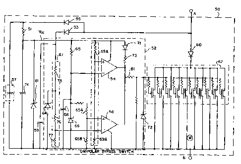
With reference to Figure l0, an exemplary
autonomous bipolar bypass circuit 80 in accordance with the
invention is coupled between the nodes A and B for use in a
-~ ~\
- 22 _ 2moozo
power system similar to the power system shown in Fig. 1.
The bypass circuit 80 includes a MOSFET 84, a MOSFET 86, a
logic and drive circuit 82, a capacitor 88, a capacitor 90,
a resistor 92, a diode 94, a diode 96, a diode 98, and a
diode 99. The MOSFETs 84 and 86 are connected in series
opposition across nodes A and B and each include internal
anti-parallel diodes integral within their structure.
The node A is coupled to the anodes of the diode
98, the diode 96 and the drain of the MOSFET 84. The
cathodes of the diodes 98 and 96 are coupled to the
cathodes of diodes 99 and 94, respectively. The node B is
coupled to the anodes of the diodes 99 and 94 and the drain
of MOSFET 86. The sources of the MOSFETs 84 and 86 are
coupled to each other and to a first terminal of capacitor
88, a first terminal of the capacitor 90, and a first end
of resistor 92. A second end of resistor 92 is coupled to
a second end of the capacitor 90, the logic and drive
circuit 82, and the cathode of the diode 99 (node Fj. The
second end of capacitor 88 is coupled to the node Vcc and
the logic and drive circuit 82. The sources of the MOSFETs
84 and 86 are also coupled to logic and drive circuit 82.
The gates of the MOSFETs 84 and 86 are coupled to the logic
and drive circuit 82.
The operation of bypass circuit 80 is similar to
bypass circuit 50. The capacitor 88 captures a positive
voltage across the SCR 34 via the diode 96 and the integral
diode of the MOSFET 86. The capacitor 88 also captures the
negative voltage across the SCR 34 via the diode 94 and the
integral diode of MOSFET 84. The voltage associated with
capacitor 88 is provided at the node Vcc to the logic and
drive circuit 82.
The filtered voltage at the node F also is
provided to the logic and drive circuit 82. The positive
filtered voltage is provided from node A via the diode 98.
The negative filtered voltage is provided from node B via
the diode 99. Therefore, the voltage appearing across the
capacitor 90 is full wave rectified by diodes 98, 99 and
--
- 23 -
the integral diodes associated with the MOSFETs 84 and 86.
The capacitor 90 and the resistor 92 provide an RC time
constant similar to the resistor 51 and the capacitor 59
discussed with reference to Fig. 3. This time constant is
typically approximately 15 milliseconds which keeps the
filtered voltage high for a long enough period of time so
that the logic and drive circuit 82 does not turn MOSFETs
84 and 86 ON during a fully asymmetric first half cycle of
fault current. Thus, the RC time constant for the
capacitor 90 and the resistor 92 is comparable with the
period of the line frequency.
When the voltage at the node Vcc is greater than
7.5 volts and the voltage at the node F is below 2.0 volts,
the logic and drive circuit 82 provides a positive gate
voltage in excess of the threshold voltage at the gates of
MOSFETs 84 and 86. When MOSFETs 84 and 86 are turned ON,
current flow in either direction is allowed across nodes A
and B through the MOSFETs 84 and 86. When the MOSFETs 84
and 86 are turned OFF, current flow is prevented through
the MOSFETs 84 and 86. The ON resistance of the MOSFETs 84
and 86 should be selected so that the voltage drop across
nodes A and B at maximum DC follow current does not exceed
approximately .5 volts. The maximum voltage drop across
each MOSFET 84 and 86 in the ON state is approximately .25
volts. Thus, when the MOSFETs 84 and 86 have positive
voltage in excess of the gate threshold voltage applied
between the gate and source, they become essentially
symmetrical resistive elements for current of either
polarity, shunted for current in one direction by the
integral diodes.
With reference to Fig. 1l, a more detailed
schematic of the autonomous bipolar bypass circuit SO
includes similar components to those discussed with
reference to Fig. 10. However, MOSFETs 84 and 86 are each
comprised of eight MOSFETs such as IRFZ 44 MOSFETs
connected in parallel. The operation of the logic and
drive circuit 82 is similar to that discussed with
2~,10U~a
- 24 -
reference to the logic and drive circuit 52 with reference
to Fig. 9. The capacitor 88 is comprised of four 5.0 ~cF
polypropylene capacitors.
With reference to Fig. 12, a non-autonomous
bypass circuit 110 is shown coupled between the nodes A and
B. The bypass circuit 110 has applications which require
that high voltage switches with capabilities greater than
MOSFETs 84 and 86 be used. However, these high voltage
type switches, such as insulated gate bipolar transistors
(IGBT), cannot by themselves provide a sufficiently low
voltage drop to turn off an SCR and therefore require an
additional voltage biasing source to divert the current
from the SCR. The additional voltage bias source can
conveniently be provided by independent power supplies.
Thus, in applications where independent power supplies are
available, the circuit 110 provides a turn off circuit with
high voltage control capability. The bypass circuit 110
further provides logic for driving the SCRs 34 and 35.
Bypass circuit 110 includes a drive and logic circuit 112,
a drive and logic circuit 114, a power supply 116, a power
supply 118, a resistor 120, a resistor 122, a diode 124, a
diode 126, an IGBT 128, an IGBT 130, a capacitor 132, and a
capacitor 134.
The node A is coupled to the emitter of the IGBT
130, a terminal of the drive and logic circuit 112, the
power supply 116, and the capacitor 132. The node B is
coupled to the emitter of the IGBT 128, a second terminal
of the drive and logic circuit 114, the power supply 118,
and the capacitor 134. The collector of the IGBT 130 is
coupled to the cathode of the diode 124, and the anode of
diode 124 is coupled to a first end of the resistor 122 and
the positive terminal of the capacitor 134. The second end
of the resistor 122 is coupled to the positive terminal of
power supply 118 and a first input of the drive and logic
circuit 114. A first output of the drive and logic circuit
114 is coupled to the gate of the IGBT 128. A second
output is coupled to the gate of the SCR 34. The collector
2110U~0
of the IGBT 128 is coupled to the cathode of diode 126.
The anode of diode 126 is coupled to the positive terminal
of capacitor 132 and a first end of resistor 120. A second
end of resistor 120 is coupled to the positive terminal of
5 power supply 116 and a first input of the drive and logic
circuit 112. The gate of IGBT 130 is coupled to a first
output of the drive and logic circuit 112. The gate of SCR
is coupled to a second output of the drive and logic
circuit 112. The bypass circuit 110 is typically for use
10 with an ISP 30 having a maximum DC blocking voltage of 200
volts, a maximum DC follow current of 150 amps, an AC
bypass capacitor of 6,500 microfarad (~CF), an SCR
triggering voltage of 300 volts, and a primary auxiliary
power source of 110 volts DC. The power supplies 116 and
15 118 are typically 15 volt power supplies.
The logic and drive circuits 112 and 114 are
similar to the logic and drive circuit 82. However, the
logic and drive circuits 112 and 114 are responsible for
driving the SCRs 34 and 35 and the IGBTs 128 and 130. The
20 logic and drive circuit 114 operates the same with respect
to the SCR 34 as the logic and drive circuit 112 operates
with respect to the SCR 35. Specifically, taking the above
typical example for illustration, when the forward voltage
across SCR 34 is greater than 300 volts, the logic and
25 drive circuit 114 provides a drive pulse to the SCR 34.
The duration of this drive pulse is sufficient to ensure
that the SCR 34 triggers into conduction, and typically
could be 30~s. The SCR 34 turns ON in response to this
drive pulse. Within a set period, which typically may be
30 80 milliseconds, following the triggering event, the
circuit 114 drives the SCR 34 in response to a forward
voltage of greater than 5V across nodes A and B.
When the circuit 110 is required to unlatch or
turn OFF the SCR 34, the IGBT 128 is turned ON for a period
35 at least equal to the SCR turn-off time and typically .5
milliseconds and then turned OFF. During the period in
which the IGBT 128 is turned ON, the DC follow current is
211Q0'~f~
- 26 -
diverted from the SCR 34 through the capacitor 132, the
diode 126 and the IGBT 128. This diversion results in a
reverse voltage of approximately 11 volts across the SCR 34
(15 volts minus the voltage drop across the diode 126 and
IGBT 128 which is typically about 4 volts). The power
supply 116 provides the proper reverse biasing voltage for
the capacitor 132.
When the SCR 34 is reverse biased for a period at
least equal to the SCR turnoff time, the SCR 34 is
effectively turned OFF. When the drive voltage to the IGBT
128 is removed, the SCR 34 has regained its forward
blocking capability and the flow of DC follow current is
prevented. The operation for unlatching the SCR 35 is
similar to that for the SCR 34 with IGBT 130 operated to
unlatch or turn OFF the SCR 35.
A more detailed schematic of the bypass circuit
110 is given in Fig. 13. The bypass circuit 110 includes
the IGBT 130, the diode 124, the power supply 118, the
resistor 122, the capacitor 134, the logic and drive
circuit 112, the IGBT 128, the diode 126, the power supply
116, the resistor 120, the capacitor 132 and the logic and
drive circuit 114. The logic and drive circuit 114 is
similar to the logic and drive circuit 112.
Logic and drive circuit 114 which controls the
SCR 34 and the IGBT 128 includes a 5 volt comparator 140, a
300 volt comparator 142, an OR gate 144, a level shifter
146, an AND gate 150, and a drive pulse generator 152.
Logic and drive circuit 114 also includes a pulse generator
151, a .3 volt comparator 156, a 3 volt comparator 158, a 5
volt comparator 160, an AND gate 162, a 5 microsecond delay
circuit 164, an AND gate 168, a resistor 170, and an FET
172. The node A is coupled to the positive input of the 5
volt comparator 140, the 300 volt comparator 142, and the
.3 volt comparator 156. The positive terminal of the 5
volt comparator 160 is coupled to the collector of the IGBT
128. Node A is also coupled to the negative terminal of
the 3 volt comparator 158.
/~.
- 2~ - ~110(~~d
For the SCR 34 to be fired for the first time,
the SCR 34 must have a forward voltage across the nodes A
and B of 300 volts or greater. SCR 34 may be fired within
80 milliseconds of the first time firing whenever the
voltage from nodes A and B is greater than 5 volts.
An inductor 48A is connected in series with the
capacitor 49 across nodes A and B. The SCR firing control
circuit is arranged so that whenever the SCR is initially
fired from the specified "high voltage" trigger level, such
as 300V, the back-to-back SCRs 34 and 35 are kept
essentially in continuous conduction, until all the energy
initially stored in the AC bypass capacitor 49 of the ISP
has substantially been dissipated, which may take a
multiple number of oscillatory cycles for completion.
The total discharge period is determined by the
natural oscillation frequency of the capacitor 49 with the
inductor 48A. This period typically could be 20 to 30
cycles of oscillation, which typically might take a total
time of about 80 milliseconds. The period could be
significantly longer or shorter, depending on the
particular design.
The inductor 48A in series with the AC bypass
capacitor 49 is necessary because the energy stored in the
bypass capacitor 49 at the SCR triggering instant is
relatively high, in a high voltage ISP. Without this
inductor, the capacitor would "dump" all its energy into
the SCR 34 or 35, within a short time (a few tens of
microseconds) after the SCR is triggered. This is
acceptable at low voltage, where neither the energy stored
in the capacitor, nor the instantaneous SCR voltage, are
too great. At high voltage, however, a rapid dump of a
large amount of energy from the capacitor 49 would damage
or destroy the SCR. The inductor 48A prevents an immediate
"energy dump" from the capacitor 49. It greatly alleviates
the stress on the SCR 34 or 35 by letting the capacitor 49
dissipate its energy slowly, over a multiple number of
cycles of decaying oscillation.
- 28 -
The circuitry that controls the triggering of the
SCRs 34 or 35 ensures that once the oscillatory discharge
is set in motion (by initially firing an SCR), the
combination of SCRs 34 and 35 are then kept in essentially
continuous conduction (i.e., without the instantaneous
blocking voltage applied to them being allowed to rise
above a few volts), until the oscillation has been
completed.
Without this feature, the "internally generated"
oscillation would be reflected from the ISP 30 back to the
connected system, rather than being kept as an "internal
event" within the ISP. Since the purpose of the ISP is to
be a passive blocking/shunting device as far as the
external system is concerned, it is undesirable that the
internal oscillatory discharge of the capacitor 49 should
be "seen" by the external system.
After the oscillation is finished, the SCR 34 is
only fired by first time conditions. A first time firing
is specifically described as follows. When 300 volts
occurs over the nodes A and B, the output of 300 volt
comparator 142 is a logic high. When the output of the 300
volt comparator 142 is a logic high, the output of OR gate
144 is a logic high. This logic high signal is provided
for 80 milliseconds by the timer 148 and provided to AND
gate 150. The output of the 5 volt comparator 14o is also
provided to AND gate 150. When the timer 148 and the 5
volt comparator 140 both provide a logic high to the AND
gate 150, the AND gate 150 provides a logic high to drive
pulse generator 152. In response to the signal from the
output of the AND gate 150, the drive pulse generator 152
provides a 30 microsecond drive pulse to the SCR 34. Thus,
whenever the SCR 34 voltage exceeds 300 volts, a first
pulse is delivered to its gate, turning it 0N. Within the
subsequent 80 millisecond period set by the timer 148, the
SCR 34 is fired whenever its voltage exceeds 5 volts,
ensuring that the voltage across the SCR 34 will not exceed
5 volts while the capacitor 49 completes its oscillatory
w ~ ~ 2110020
- 29 -
discharge. The output of the 300 volt comparator 142 is
provided to a similar OR gate through a level shifter in
logic and drive circuit 112 similar to the level shifter
146, starting a similar 80 millisecond timer for the SCR 35
and enabling it to be fired whenever its voltage attempts
to exceed 5V.
The OR gate 144 also provides a logic high to the
timer 148 when either the AND gate 162 or the level shifter
146 provides a logic high. The level shifter 146 provides
a logic high when a 300 volt comparator in the logic and
drive circuit 112, which is similar to the comparator 142,
outputs a logic high. This later event ensures that the
AND gate 150 is enabled for an 80 millisecond period
following first-time firing of the SCR 35, should this SCR
be the first SCR to be fired, in readiness for the above-
described oscillatory current discharge of the capacitor 49
to reverse polarity and require the SCR 34 to conduct.
The IGBT 128 is also controlled by the logic and
drive circuit 114. The IGBT 128 is turned ON when the SCR
34 becomes stuck in a conduction state by an external power
source. The AND gate 166 operates to turn IGBT 128 ON.
Specifically, the pulse generator 151 supplies a pulse of
about 300 microseconds duration 100 milliseconds after the
last firing pulse to the SCR 34 produced by AND gate 150.
Thus, the AND gate 166 is enabled by the pulse generator
151 100 milliseconds after the SCR 34 receives its last
pulse.
The AND gate 168 provides a logic high to the AND
gate 166 whenever the comparators 156 and 158
simultaneously provide logic highs. The comparator 156
provides a logic high to AND gate 168 when the voltage
across nodes A and B is greater than .3 volts. The
comparator 158 provides a logic high whenever the voltage
across nodes A and B is less than 3 volts. Thus, the AND
gate 168 provides a logic high when the voltage across
nodes A and B is between .3 volts and 3 volts. When both
AND gate 168 and delay circuit 151 output a logic high, the
- 30 - 211000
AND gate 166 outputs a logic high to the one millisecond
monostable 157.
The one millisecond monostable 157 provides an
output high signal for a set period of 1 millisecond which
is a sufficient time to ensure that the SCR 34 turns OFF.
The output of the 1 millisecond monostable is provided
through the resistor 170 and turns the IGBT 128 ON. At the
end of the 1 millisecond period, the output of the
monostable 157 goes low and turns OFF the IGBT 128.
This signal is also provided through delay
circuit 164 to the AND gate 162 after a 5 microsecond
delay. The AND gate 162 provides a logic high signal to
FET 172 when the voltage across the IGBT 128 is greater
than 5 volts and the delay circuit 164 outputs a logic
high. The AND gate 162 turns the FET 172 ON and hence
turns the IGBT 128 OFF if the voltage across the IGBT
becomes greater than 5 volts after a period of 5
microseconds from the turning ON of the IGBT 128. The AND
gate 162 also provides the signal to the OR gate 144. The
signal provided to the OR gate 144 refires the SCR 34 if
the IGBT 128 is ~~prematurely~~ turned OFF due to the voltage
across it becoming greater than 5V during its otherwise
intended conduction period. The AND gate 162 ensures that
excessive currents are not driven through the IGBT 128.
The operation of logic and drive circuit 114
ensures that the IGBT is driven appropriately.
Specifically, the logic and drive circuit 114 drives the
IGBT 128 when a bypass closure of the IGBT 128 has not
taken place since the last firing pulse provided by the
drive pulse circuit 152, no gate drive pulses from circuit
152 have occurred within 100 milliseconds, and the voltage
across nodes A and B is less than approximately 3.0 volts
positive but greater than .3 volts positive. The no bypass
closure condition ensures that unnecessary closures of the
IGBT 128 do not take place when SCR 34 or SCR 35 is already
providing the blocking function between nodes A and B. The
100 millisecond condition ensures that the IGBT 128 is
2110020
- 31 -
activated only when an SCR is "stuck" in conduction due to
DC follow current from an external supply. The less than
3.0 volts positive and greater than .3 volts positive
condition ensures that the IGBT 128 is turned ON only when
the SCR 34 is in conduction. Turning ON the IGBT 128 when
the SCR 35 is conducting, which would be represented by a
negative voltage across nodes A and B, therefore less than
0.3V positive, may produce undesirable high circulating
current.
Typically, the IGBT 128 and the IGBT 130 could
each be comprised of 6 parallel IRGPC50F 70 Amp, 600 volt
IGBT's or 10 parallel IRGBC40F 49 Amp, 600 volt IGBT's.
The IGBTs 128 and 130 could also typically be each
comprised of a single high current IGBT module rated at
several hundred amps. With reference to the foregoing
description of Fig. 13, it is understood as with the
circuits in all the figures that the operating levels,
component selection and timing periods could be widely
different without alternating the basic principles of the
circuit 110.
operation of the circuits of Fig. 13 is
illustrated diagrammatically in Fig. 14. Prior to time to,
the ISP has a DC bias voltage V~ applied, and the forward
blocking voltage across the SCR 34 is Vp~. At time to, a
surge current flows into the ISP. As a result of this
current, the voltage across SCR 34 increases.
At time ti, the voltage across SCR 34 reaches the
trigger level, which typically could be several hundred to
several thousand volts, and SCR 34 turns ON. The output of
the 80 millisecond timer 148 assumes a logic high at time
t" and the capacitor 49 proceeds to resonate with the
inductor 48A, producing an underdamped oscillating current
throughout the period t, to t2. This current flows freely
through the back-to-back SCRs 34 and 35, each SCR
commencing conduction as soon as its anode voltage reaches
a voltage of about 5V, in each successive half-cycle.
2110020
- 32 -
The total current through the SCRs is the sum of
the applied fault current and the oscillating current in
capacitor 49. At time t2, the SCR 34 turns on for the
"final" time, the current in this SCR now becoming
unidirectional as a result of the DC current flowing into
the ISP 30.
The 100 millisecond-delayed pulse circuit 151
starts a fresh time-out period as each SCR firing pulse is
initiated. Since no SCR firing pulses occur after time t2,
the output of the 100 millisecond delayed pulse circuit 151
assumes a logic high at time t3, which occurs approximately
100 milliseconds after time t2.
The duration of the logic high pulse of the 100
millisecond delayed pulse circuit is about 300
microseconds. During this period the AND gate 166 is
enabled. The output of AND gate 168 is already high at
time t3, because the voltage across SCR 34 at this time
falls within a 0.3 to 3.0V window. Therefore, the output
of AND gate 166 assumes a logic high value at time t3, the
output of the 1 millisecond monostable assumes a logic high
value, and the IGBT 128 is turned on. The voltage across
SCR 34 is now reversed by the DC bias voltage across the
capacitor 132, and the current in SCR 34 diverts into the
IGBT 128.
During the period t3 to t4, the current flowing in
IGBT 128 increases, as capacitor 132 sends a charging
current into capacitor 49, as well as into the external
system. At time t4 the 1 millisecond monostable times-out,
the drive voltage is removed from IGBT 128, which turns
off, and the voltage across the SCR 34 starts to re-
establish to the applied DC value, VDC~
With reference to Fig. 15, a portion of an ISP
circuit includes a shunt path comprising a MOSFET 269, a
resistor 267 and a diode 271 which may be used with the
bypass circuit 50 in an ISP. The shunt path is controlled
by a circuit 260. ISPs are susceptible to a pumped up
voltage across nodes A and B from inductance associated
2110020
- 33 -
with the external voltage source 37 represented by an
inductor 261 in Fig. 15, as well as the internal inductance
of the ISP, which will contain energy when the bypass
circuit 50 turns the current OFF.
This stored energy can generate a voltage across
the nodes A and B which can retrigger the SCR 34 after the
bypass circuit 50 turns OFF the SCR 34. Thus, the inductor
261 can cause a continuous repeating cycle of operation
under which the SCR 34 repeatedly turns ON and OFF.
The circuit 260 includes an AND gate 262, a
comparator 264, and a delay circuit 265. The FET 269 could
be replaced by an IGBT or other type of switching device.
The diode 263 is not a necessary part of the supply 37.
The delay circuit 265 receives a signal at node E from the
logic and drive circuit 52 within the bypass circuit 50
(Fig. 3). The signal at node E turns the bypass switch ON
and OFF as described above. When the signal turns the
bypass switch from ON to OFF, the delay circuit 265
provides a logic high to the AND gate 262. The signal from
the delay circuit 265 provides a "watch period" which
enables the AND gate 262. If the voltage across the SCR 34
becomes greater than a preset reference voltage which would
typically be about 8V for the bypass circuit 80 of Fig. 11,
and typically several hundred volts for the bypass circuit
110 of Fig. 13, the comparator 264 provides a logic high to
the AND gate 262. The AND gate 262 outputs a logic high to
the FET 269.
When the FET 269 is turned ON, a shunt path or
clamp circuit including the resistor 267 and FET 269 is
provided between the nodes A and B and the resistor 267
shunts the current across the node A and the node B. The
shunt path arrests the rise of voltage across the node A
and the node B. Thus, the inductor 261 is not able to
retrigger the SCR 34. The resistor 267 is sized so that
the combined voltage developed across it, the transistor
269 and the diode 271 with maximum DC follow current
flowing through it is less than the level which switches
- 34 -
the output of comparator 264 to a logic high. When the
voltage across the nodes A and B falls below a voltage
which is less than the above preset voltage reference, the
comparator 264 outputs a logic low and the AND gate 262
turns OFF the FET 269.
The comparator 264 is designed with hysteresis to
provide proper operation. For example, the comparator 264
provides a logic high when the voltage across the SCR 34 is
greater than 8 volts. The comparator 264 provides the
logic high until the voltage at the positive input falls
below 7.5 volts. The resistor 267 may be successively
connected and disconnected multiple times within the "watch
period", as energy from the inductor 261 successively pumps
up the voltage across the capacitor 49, the FET 269 is
turned on, the capacitor 49 discharges into the resistor
267, the MOSFET 269 is turned off, and the cycle repeats
until all the energy stored in the inductor 261 is
dissipated.
The circuit 260 is typically designed with the
following performance specifications. The nominal SCR
trigger value of the ISP circuit is 12 volts, the maximum
DC bias voltage in source 37 is 5 volts, the maximum DC
bias current is 40 amps, the maximum value of the
inductance 261 of the circuit external to the ISP is 25
millihenries, and the minimum value of the capacitor 49 of
the ISP is 10,000 ~CF. The value of the resistor 267 is
typically .15 ohms. Typically, the delay circuit 265
provides a watch period of at least 400 milliseconds. In
general, the duration of the watch period is set to ensure
that all energy stored in the inductor 261 is dissipated by
the operation of the clamp circuit when the inductor 261
and the DC follow current simultaneously have their maximum
possible design values.
kith reference to Fig. 16, a more detailed
schematic of the circuit 260 is shown. The circuit is
essentially the same as previous bypass circuits discussed
21I0~3~a
- 35 -
with reference to Fig. 11. Only the additional circuitry
associated with the circuit 260 is described below.
The circuit further utilizes three MOSFETs which
operate to provide the function of the FET 269 discussed
with reference to Fig. 15. Typically, the comparator 264
and the delay circuit 265 are comprised of LP339 open
collector comparators. As described with reference to Fig.
11, the AND gate 162 can be eliminated if these components
are used.
The three MOSFETs representing the FET 169 are
coupled to a diode 271, a diode 272 and a resistor 267.
The MOSFETs are controlled by FET transistors 276A (N-
channel) and 276B (P-channel) coupled to the comparator 264
and the delay circuit 265.
The operation of the circuit 260 of Fig. 16 is
illustrated in Figs. 17 and 18, which show waveforms of the
voltage across the bypass switch after it turns off and the
voltage clamp circuit 260 is activated, due to energy
stored in the DC source inductance 261.
The waveforms in Fig. 17 are for a relatively low
value of DC follow current. The clamp circuit switches on
and off just three times, before the energy in the DC
source inductor 261 is exhausted.
The waveforms in Fig. 18 are for a much higher
value of DC follow current. The clamp circuit switches on
and off multiple times before the energy in the DC source
inductance 261 is exhausted.
With reference to Fig. 19, an alternative voltage
clamp circuit 277 for use with a bypass circuit such as
circuit 80 discussed with reference to Fig. 10 is shown.
The alternative clamp circuit includes a resistor 278, a
MOSFET 279, a MOSFET 280, and a resistor 281. The MOSFET
84 and MOSFET 86 each belong to the main bypass switch as
shown in Fig. 10. The clamp circuit could be used to
replace the FET 269 and resistor 267 and the diodes 271 and
272 shown in Fig. 16. The circuit 277 utilizes two MOSFETs
:.~ ~ ~ ~ ~l~,t~02~
- 36 -
and eliminates the diodes 271 and 272 in the bypass path in
Fig. 16.
With reference to Figs. 20 through 22,
alternative embodiments of ISPs are shown which utilize
asymmetrical gate turn off thyristors (GTOs). GTOs are
commercially available with forward voltage ratings of up
to 4500 volts and rated peak turn off current up to several
1000 amperes.
With reference to Fig. 20, GTOs 382 and 384
replace SCRs 34 and 35 in an ISP similar to the ISP 30
discussed with reference to Figs. 1-19. The GTOs 382 and
384 can be turned OFF by applying a negative pulse of
current at the gate. Thus, the use of a GTOs 384 and 382
eliminates the need for a turn off circuit such as the turn
off circuit 50 discussed with reference to Fig. 3. In the
main ISP switch 220, a logic and drive circuit would be
used to produce a negative gate pulse for turning OFF GTOs
382 and 384 when the surge condition has passed.
With reference to Fig. 21, a further main ISP
switch 385 is shown which utilizes a GTO 387, a GTO 389, a
diode 381 and a diode 383. With reference to Fig. 22, a
further embodiment of a main ISP switch 390 is shown
utilizing one GTO 392, and full bridge of diodes 393, 394,
395, and 396. Alternatively, each of the GTOs in Figs. 20
through 22 could be substituted by functionally similar
devices such as static induction thyristors or mos-
controlled thyristors.
The circuits 220, 385 and 390 are also applicable
in providing a bypass circuit for geomagnetically induced
current. In such applications, the required blocking
voltage may be in the range of several thousand volts.
These types of circuits could be applied in a manner
similar to that of the circuit discussed with reference to
Fig. 12; however, GTOs would be used rather than SCRs and
IGBTs. The disadvantages of using GTOs is that they are of
higher cost and have lower overall current ratings and
lower surge current ratings. Further, the reverse voltage
1w! :W.
2110020
- 37 -
blockage of a GTO is generally significantly less than an
SCR and the drive current provided at the gates of the GTOs
is greater, especially for turning OFF the GTO. Diodes 381
and 383 and the diodes 393, 394, 395 and 396 may be
utilized to provide reverse voltage blocking capacity.
With reference to Fig. 23, an ISP 400 is shown
which utilizes a turn off circuit 410 which turns off the
main SCRs 34 and 35. The turn off circuit 410 includes a
commutating capacitor 412, a commutating SCR 414, a
commutating inductor 415, and a commutating SCR 416. When
a logic and drive circuit similar to the logic and drive
circuit 52 or 112 and 114 determines that one of the SCRs
should be turned OFF, the logic and drive circuit fires the
commutating SCRs 414 and 416. The precharged commutating
capacitor 212 is precharged by a precharging circuit 418.
A local resonating alternating current powered by the
capacitor 412 is produced across the SCRs 34 and 35, which
turns off the appropriate SCRs 34 or 35.
The values shown in the various figures are
preferred values for a particular embodiment and are not
shown in any limiting sense. The various signal levels are
also preferred values and are not shown in any limiting
sense. Various other values or package types could be
utilized.
It is understood that the invention is not
confined to the particular construction and arrangement of
parts herein illustrated and described, but embraces all
such modified forms thereof as come within the scope of the
following claims.