Note: Descriptions are shown in the official language in which they were submitted.
2110187
Technical Field
The present invention relates to transistor mounting devices, and in particular, to
mounting clamp assemblies for electrically connecting transistors or other high-powered
devices to other circuit elements, especially where such transistors and/or devices are
5 used for cyclically operated high-powered applications.
Background of the Invention
High-powered transistors used for amplifying ultra-high frequency (UHF) and
microwave frequencies often have low input and/or low output impedances which
n~s~arily require m~t~hing network components to be placed as close as possible to the
10 transistor in order to achieve reasonable power bandwidths. Typically in order to connect
a radio frequency (RF) power transistor in an actual circuit, the flange of the transistor is
mechanically screwed to a heat sink while the base, emitter and collector tabs of the
tran~i~tor are soldered to a printed circuit board on which the necessary matçhing network
col,lponents are placed. Thus soldering is generally used as both the electrical and
15 mechani~l fa~tPning technique for such transistors.
In circuit applications which do not permit the transistor to be driven continuously,
such as the cyclical operation of power amplifiers used for cellular communications
traffic, thermal cycling stress and associated mechanical creep can lead to early failure of
solder joints, especially in high current applications having small joint cross-sections, and
20 especially where the m~terial connected by soldering have different co-efficients of
thermal expansion. The latter condition is prevalent in situations where solder is used as
the method of joining a power transistor or other high-powered device to a printed circuit
board trace.
The above-referenced conditions which can lead to thermal cycling stress and
25 mechanical creep are particularly present for solder joints between the collector output tab
of high power RF transistors, especially those that use nickel steel (known as Alloy 42)
for the output tab, and an associated circuit board trace and the tabs of the closely spaced
matching c~pacitQrs. Typical lifetimes of such solder joints when cycled at full RF power
are from two to four months in cellular communication applications, and somewhat longer
30 if power output is reduced. Identical amplifiers using the same transistors but operating
on a contlnuous basls do not exhlblt such solder ~olnt
fallures. Unfortunately, ln many appllcatlons, lncludlng such
cellular communlcatlon slgnal channel ampllflers, energy costs
are slgnlflcant and as a result, the ampllflers are operated
on a cycllcal need basls dependent on the volce trafflc.
A prlor art fastenlng technlque whlch can wlthstand
the thermal cycle stresses and mechanlcal creep assoclated
wlth lntermlttent hlgh power use ls known as brazlng. Thls
process uses hlgh meltlng temperature materlals, such as
sllver alloys, for connectlng two electrlcally conductlve
ob~ects whlch have stlll hlgher meltlng temperatures. Thls
technlque ls commonly used ln alr condltlonlng and heatlng
appllcatlons. However, the temperatures needed for conducting
the brazlng operatlon are typlcally ln excess of 800 degrees F
(ln excess of 426 degrees C). These temperatures cannot be
tolerated by power translstors nor by typlcal prlnted clrcult
boards and related components. In addltlon, other prlor art
electrlcal connectlon technlques whlch are commonly uæed ln
automotlve and home wlrlng make use of mechanlcal fastenlng
methods such as bare wlre connected wlth screws, crlmped
connectlons, posts and the llke. Such technlques are not
satlsfactory for preventlng connectlon fallures due to thermal
stress and assoclated mechanlcal creep encountered ln the
hlgh-powered translstor appllcatlons. They are also
unsatlsfactory for hlgh frequency appllcatlons (typlcally
above 400 MHz) slnce the wlre used ln such technlques
lntroduce slgnlflcant lnductance lnto the overall clrcult.
The present lnventlon provldes a solutlon for
65993-244
2 ~
mountlng such hlgh-powered translstors by use of a translstor
mountlng clamp assembly.
Summary of the Inventlon
Accordlng to a broad aspect, the present lnventlon
provldes a mountlng clamp assembly for electrlcally connectlng
an electrlcal connector tab of an electrlcal devlce to another
area, comprlslng: A) a top clamp havlng a flrst surface
dlmensloned for engagement wlth the connector tab of the
electrlcal devlce; B) a bottom clamp havlng a flrst surface
dlmensloned for engagement wlth the top clamp flrst surface
and wlth the connector tab posltloned therebetween; C) means
for mechanlcally urglng the top clamp and bottom clamp
together so as to sandwlch the connector tab between said
flrst surfaces; and D) means for electrlcally connectlng the
clamp assembly to another area.
Accordlng to a speclflc embodlment, a translstor
mountlng clamp assembly ls descrlbed whlch overcomes thermal
cycllng stress and mechanlcal creep assoclated wlth solder
~olnts used to ~oln hlgh-powered translstors to matchlng
network components mounted on prlnted clrcult boards, where
such translstors and matchlng network components are typlcally
used ln ultra-hlgh frequency (UHF) or mlcrowave-type
appllcatlons. The translstor mountlng clamp assembly provldes
a rellable electrlcal connectlon between the collector output
tab of a hlgh-powered radlo frequency (RF) type translstor and
assoclated closely spaced matchlng network components mounted
to a prlnted clrcult board. Such components are typlcally
65993-244
2110187
used in UHF and microwave power amplifiers, including class C amplifiers. For such
amplifiers the m~t~hing network components are typically mica capacitors if the
c~pacit~nce is 10 pF or greater, due to their power handling capability and high quality
factor (Q). All these components, as well as the cireuit board, undergo thermal cycling
5 stress ~oei~tPd with cyclical operation of such elass C amplifiers under high-power
conditions.
In a plt;r~lled embodiment of the present invention, the elamp assembly is used
with a six-tab power transistor. The elamp assembly for this prerelled embodiment has a
hexagonal geometry which permits fastening the colleetor output tab of the transistor to
10 the clamp assembly without contacting the ground tabs of the transistor. The hexagonal
geometry of the clamp further provides for better position control and manllf~ct~ hility
of the clamp. A T-shape clamp assembly is also described in an ~ltem~tive embodiment.
In order to permit secure mounting of the transistor and the associated network
m~t~ hing e~r~itors~ especially where the transistor tab and capacitor tab geometries may
15 vary, a conically shaped pressure contact area is formed by the top and bottom clamps.
This cone area for either the top or bottom clamp, or both, may also be knurled or
otherwise surface treated so as to have surface discontinuity (height variations) to
f~-ilit~te pres~.lre equalization associated with varying tab thicknesses. In a prerelled
embodiment, the upper surface of the bottom clamp has a stepped circular concave20 geometry which secures the tabs at the step edges. Shims may also be used to increase
the effective thicknPs~ of one or more connector tabs which are significantly thinner than
the thick~st tab secured by the clamp assembly.
In addition, this well defined contact arrangement faeilit~t~s repeatability of
assembly for the required m~t~hing network components . Since capacitance values are
25 critically determined by the electrical paths from the caraeitors to the power transistor,
this repeatable assembly ensures substantially consistent electrical path lengths which
greatly facilitate overall manufacture of the amplifier.
The top and bottom clamp each have a central bore, with the bore of the bottom
clamp tapped. A machine screw is used to secure the top and bottom clamp together with
30 the mounting tabs of the transistor and capacitor secured in the contact area. A
wide extending tab is fastened to the top clamp by the same machine screw.
A shoulder washer ls typlcally used to place the
clamp assembly onto an associated heat slnk. Flnally, a
Bellevllle washer ls typlcally used to absorb stress
assoclated wlth dlfferentlal expanslon of dlsslmllar
materials, whlle gold platlng of the clamp assembly components
ls used to mlnlmlze corroslon and oxldatlon.
The translstor mountlng clamp assembly ls attached
to the clrcult board by solderlng the extendlng tab to a
clrcult board trace. The extendlng tab may alternatively be
dlrectly connected to other clrcult components. The resultlng
conflguratlon læ found to be extremely rellable ln operatlon
regardless of the thermal cycllng assoclated wlth lntermedlate
use of the assoclated ampllfler. A lug may also be formed on
the extendlng tab to provlde DC power to the connected
components and thereby reduce cycllcal heatlng assoclated wlth
DC current flow through the power translstor.
It ls therefore a broad ob~ect of the present
lnventlon to provlde a mountlng clamp assembly for
electrlcally connectlng an electrlcal connector tab of an
electrlcal devlce to another area.
Ob~ects of the Inventlon
It ls another ob~ect of the present lnventlon to
provlde a translstor mountlng clamp assembly for mechanlcally
and electrlcally mountlng a hlgh-power translstor to a clrcult
board wlth lts assoclated matchlng components, partlcularly
for use ln hlgh-power ampllflers whlch are cycllcally
operated, thereby causlng thermal stress.
A further ob~ect of the present lnventlon ls to
65993-Z44
~1 1 0 1~
provlde a clamp assembly of the above descrlption whlch ls
hexagonal ln shape so as to allow fastenlng of the center
collector tab of the translstor wlthout touchlng the
assoclated ground tabs.
A stlll further ob~ect of the present lnventlon ls
to provlde a clamp assembly of the above descrlptlon whlch ls
able to accommodate varlatlon exhlblted by translstor and
assoclated component tab geometrles by use of a conlcal
pressure contact area formed by top and bottom clamps formlng
part of the clamp assembly, further whereln thls contact area
lncorporates stepped reglons for securlng the mountlng tab of
the translstor and matchlng components.
Another ob~ect of the present lnventlon ls to
provlde a clamp assembly of the above descrlptlon, whereln the
stepped reglon of the contact area achleves repeatablllty of
electrlcal path lengths so as to facllltate matchlng component
value selectlon.
Another ob~ect of the present lnventlon ls to
provlde a clamp assembly of the above descrlptlon that also
uses shlms to lncrease the effectlve thlckness of connector
tabs
5a
65993-244
,
~110187
which are signific~ntly thinner than the thickest tab secured by the clamp assembly.
A still further object of the present invention is to provide a clamp assembly of the
above description, further having a tab forming part of the clamp for supply DC power
and thereby reducing the thermal stress at the transistor tab.
S A further object of the present invention is to provide a mounting clamp assembly
for connecting high powered electrical devices to other devices.
Other objects of the present invention will in part be obvious and will in part
appear hereinafter.
Brief Description of the Drawings
For a fuller understanding of the nature and objects of the present invention,
reference should be made to the following detailed description taken in connection with
the accol.lparying drawings, in which:
Figure 1 is a top plan view of the transistor mounting clamp assembly according to
the present invention, showing the assembly secured to a circuit board with electrical and
mech~ni-~l connection to a power transistor and its associated network element
c~p~citors. The view does not show some of the elements forming the mounting clamp
assembly for purposes of clarity.
Figure 2 is a side cross-sectional view of the transistor mounting clamp assembly
with the elements not shown in Figure 1 included in Figure 2. This figure is generally
taken along line 2-2 of Figure 1.
Figure 3 is a bottom view of the top clamp of the transistor mounting clamp
assembly.
Figure 4 is a side elevational view of the top clamp.
Figure S is a top plan view of the bottom clamp of the transistor mounting clampassembly.
Figure 6 is a side elevational view of the bottom clamp.
Figure 7 is a top plan view of the extending tab forming part of the transistor
mounting clamp assembly.
Figure 8 is a side elevational view partially in cross-section of the extending tab.
Figure 9 is an enlarged view of the bottom clamp showing how a mounting tab is
2110187
secured at the stepped regions.
Figure 10 is a top plan view of an alternate embodiment of the top clamp.
Figure 11 is a side view of the top clamp shown in Figure 10.
Figure 12 is a top plan view of an alternate embodiment of the bottom clamp for
S use with the top clamp shown in Figures 10 and 11.
Figure 13 is a side view of the bottom clamp shown in Figure 12.
Figure 14 is a top view of the alternate clamp assembly with the top clamp not
shown, but with the lock washer shown in phantom.
Figure lS is a side view of the alternate clamp assembly.
Best Mode for Carr,ving Out the Invention
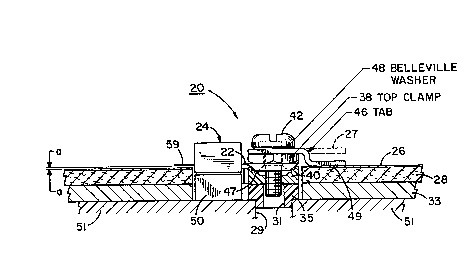
As best seen in Figures 1 and 2, a transistor mounting clamp assembly 20
comprises a number of con~tituent elements as described below which, in combination
function to provide secure mech~ni~l and electrical connection of a collector connector
tab 22 of a power transistor 24 to the metallized trace 26 of printed circuit board 28. The
lS transistor also has an emitter tab 55 and four base tabs 56, 57, 58 and 59. The mounting
clamp assembly also ensures reliable mechanical and electrical connection of mounting
tabs 30 and 32 of m~tching network capacitors 34 and 36. The con~titllent elem~,nts of
the transistor mounting clamp assembly include a top clamp 38, a bottom clamp 40, a
machine screw 42 which is threaded into threads 53 within the central orifice 44 of
bottom clamp 40, an optional non-conductive shoulder washer 35, an extending tab 46,
and a Belleville or lock washer 48, all as best seen in Figures 2, S and 6.
As seen in Figures 1 and 2, the transistor mounting clamp assembly and the
~oci~ted transistor 24 are positioned over a recess 21 in printed circuit board 28 and
metal ,~hiel(ling box 33, the recess having segments 70, 71, 72, 73, 74, 75, 76, 77, 78,
and 79. Thus collector tab 22 and clamp assembly 20 only make electrical contract with
circuit board 28 at region 49; that is, where extending tab 46 is soldered or otherwise
connected to trace 26.
The top clamp 38 as seen in Figures 3 and 4 includes a beveled cone-shaped
surface 39 for securing engagement with transistor collector tab 22 as best seen in Figures
1, 2 and 9. The top clamp has a central bore 23 which may be countersunk at region 25.
2110187
In this configustion, transistor tab 22 at region 47 is mechanically secured between top
clamp 38 and bottom clamp 40, as best seen in Figures 2 and 9. Machine screw 42 and
Belleville washer 48 mPch~nic~lly secure the overall mounting clamp assembly in its rigid
configuration by threading the machine screw 42 into the threaded region 53 of bottom
S clamp 40. The m~chine screw may also pass into a portion of bore 31 formed within
shoulder washer 35 which in turn is mounted atop a cutout 29 in heat sink 51. Washer
35, which is preferably made from Teflon~ or other non-electrically conductive m~tPri~l,
electri~lly isolates clamp assembly 20 from the heat sink and thus the ground plane
formed by metal box 33, while providing a secure mechanical rest for the clamp
10 assembly.
As seen in Figure 2, the extending tab 46 is mechanically sandwiched between theBelleville washer 48 and the upper surface of top clamp 38 so as to make intim~te
mP~h~nir~l and electrical connection thereto and thus secure electrical connection with
tr~n~i~tor collector tab 22. The extending tab is in turn soldered at region 49 to the
mPt~lli7e~ trace 26 of printed circuit board 28. Region 49 could ~ltPrn~tively be
mech~ni~lly secured to trace 26 or could be directly attached to other circuit components
(not shown). The extending tab may include a lug 27 (shown in phantom) for supplying
DC power to the clamp assembly. By supplying DC power to the clamp assembly,
overall power variation in collector tab 22 is reduced with corresponding reduction in
20 thermal expansion/contraction.
The transistor flange 50 is internally connected to the transistor and thus forms
part of transistor 24. This flange is secured to a heat sink 51 by machine screws (not
shown) passing through orifices 52 and 54.
As seen in Figures l, 3 and 4, top clamp 38 is preferably hexagonal in shape so as
25 to provide merh~nical and electrical engagement with the collector tab 22 of transistor 24
and the mounting tabs 30 and 32 of matching network capacitors 34 and 36, but so as not
to contact the transistor base tabs 56 and 58. Base tabs 56 and 58 are shown respectively
notched at regions 63 and 65 so as to provide additional clearance from the clamp
assembly. The hexagonal geometry makes the clamps rotary symmetric which f~cilit~tPs
30 manufacturing since such clamps can be manufactured on a screw machine. Other rotary
symmetric geometries may also be used.
2110187
It has been found that the transistor mounting clamp assembly shown in Figures 1and 2 achieves reliable electrical and mechanical connection of transistor tab 22 and
c~pacitor tabs 30 and 32 to the printed circuit board met~lli7ed trace 26. This connection
is not subject to fatigue and deterioration associated with thermal cycling of the transistor
5 during its normal operation. In particular, for power transistors used in UHF and
miclowave applications and especially class C amplifiers that are cyclically energi_ed and
de-energi_ed, prior art techniques have caused solder deterioration if the collector tab 22
is soldered to the m~t~lli7ed trace 26. It is believed that the problem is in part due to the
therrnal cycling of the co---ponents and in particular, to the different thermal coefficients
10 of expansion between the metal used to form the collector tab of the transistor and that
used on the printed circuit board, as well as the solder which is used to mechanically and
electrically connect those components to one another. Solder gran~ ri7~tion can occur as
a result of thermal cycling which in turn increases the resistance at the solder junction,
which in turn can lead to rapid catastrophic mechanical and electrical connection failure.
The present invention by means of the top and bottom clamps which wedge the
tabs between steps 41 in bottom clamp 40, mechanically and electrically secure the tabs.
Surface 64 of bottom clamp 40 has sharp edges 43, 45 and 61 formed by steps 41. As
seen in Figure 9, these edges form depressions in tabs 22, 30, and 32, where the tabs
contact these edges (tab 32 not shown in Figure 9) so as to resist movement of tabs as the
20 tabs and the associated clamps 38 and 40 expand and contract due to cycled operation of
transistor 24. By so securing tabs 22, 30 and 32, the electrical paths therebetween and
to solder region 49 remain relatively fixed and repeatable from in~t~ tion to in~t~ tion.
This repeatability is maintained during cycled operation of the transistor for easier
in~t~ tion since the capacitance values of capacitors 34 and 36 can be set (typically 12
25 pF for the disclosed inst~ tion) and need not be changed during in~t~ tion. The above
result is not achievable through traditional soldering techniques. Other techniques for
electrically and mechanically connecting components to one another which undergothermal expansion and contraction, such as bra_ing, are not possible for configuring
power transistors in the current configuration due to the high temperatures associated with
30 the brazing process which would be destructive to the transistor and matching network
capacitors and printed circuit board.
2110187
If any tab secured by the clamp assembly is significantly thinner than the thickest
tab (such as thinner tab 22 shown in Figure 9 - note orientation of tab 30 for purposes of
illustration only and does not correspond to orientation shown in Figure 1), a shim 67 can
be placed adj~,nt the thinner tab to increase its effective thickness to approximate the
thick~,st tab, such as shown by shim 67 in Figure 9. The shim is preferably made from
the same m~t~,ri~l as the thinner tab to which it is placed so as to minimi7~ differential
p~n~ion. Thus for collector tab 22, the shim is typically formed from Alloy 42.
The details of the bottom clamp are best seen in Figures 5 and 6 while the details
of the extending tab are best seen in Figures 7 and 8. It should be noted that the
Belleville spring washer or lock washer 48 serves as a mechanical buffer to absorb the
stresses on the m~r,hine screw 42 due to differential thermal coefficient of expansion of
the tli~imil~r metals associated with the transistor collector tab and the col,-ponents of the
clamp assembly and printed circuit board. Belleville washers are generally preferable to
lock washers due to the former's favorable compression length versus force
charact~,ristics, thereby allowing such washers to absorb greater expansion/contraction of
the clamp assembly.
It should also be noted that the relatively large area 49 of extending tab 46
improves the electrical and thermal conductivity between the extending tab and the
underlaid portion of the trace. In addition, the top and bottom clamps of the clamp
assembly are preferably formed from brass or similar m~t~ri~l and provide a heat sinking
function for all the connected tabs as well as the heat conductive structures associated
with the extending tab 46. This heat sinking thereby reduces the stress of the extending
tab solder joint to the met~lli7ed trace.
Although soldering of the extending tab 46 is used in the preferred embodiment,
other means for connecting the clamp assembly to the printed circuit board trace or other
co-~ponent can be used. Thus the tab need not be soldered to trace 26 but could be
secured thereto by mechanical means. A direct connection could also be made to another
component without connection to the printed circuit board.
It should be noted that the cone-shaped portion 39 of top clamp 38 may also be
knurled as shown by region 37 (Figure 4) to help secure tabs 22, 30 and 32. Dimples,
non-crossing ridges, or other surface projections can also be used to define contact areas
2110187
to increase pies~u~e against the tabs. Either or both surfaces 39 and 64 may include such
surface projections. The important feature of this securing technique is that the tabs be
slightly deformed at edge regions such as edges 43 for steps 41 in bottom clamp 40,so as
to resist movement during thermal contraction and expansion. Clamps 38 and 40 are also gold plated (see Table 1) so as to resist corrosion and oxidation.
Although not germane to the design of the mounting clamp assembly, in the
configuration shown for use in UHF applications, the geometry of the clamp assembly
causes a change in the matching capacitor values for capacitors 34 and 36 from approxi-
mately 10 pF to 12 pF. This causes an approximate 12 dB reduction in the level of
10 second harmonics at the ~mplifier output when the clamp assembly is used in association
with a class C power amplifier, together with significantly lowered third harmonics. The
various component and inst~ tion dimensions for this preferred use of the present
invention are set forth in Table 1.
TABLE 1
COMPONENT TYPE
transistor 24 SD1496
tab 22 alloy 42, gold plated
capacitors 34, 36 mica 12 pF
tabs 30, 32 silver plated
top clamp 38 m~tPri~l brass, hex-stock
finish: gold plating 50 micro
inches
bottom clamp 40 material: free cuffing brass 1/4" hex stock
finish: gold plating, 50 micro
inches
dimensions (see Figures 2,4,5-8 for reference character locations)
reference character dimension (inch)
a-a 0.011
2110187
b-b 0.03
c-c S/32 dia
d-d 0.030
e 0.089 dia through c'sink 5/32 dia x 82
f_f .288
g #50 drill and ~f2-56 UNC-2B tap through
h-h 0.012
i-i 0.024
jj 0.036
k-k 0.211 dia
1-1 0.182 dia
m-m 0.154 dia
n-n 0.125 dia
o-o 0.050
p-p 0.086
qq 0.000 datum point
r 0.072
s 0.145
t 0.216
u 0.29
v 0.125
w 0.300
x 0.48
y 0.089 dia
z 0.000 datum point
ab 0.085
ac 0.016 max radius
ad 0.016 max radius
An alternative embodiment 20' of the invention is seen in Figures 10 - 15.
2110187
Figures 10 and 11 shows that an alternative top clamp 38' can have a T-shape forsecuring the transistor collector tab 22 and the main capacitor tabs 30,32 therebeneath.
The corresponding bottom clamp 40' as seen in Figures 12 and 13 is ~lim~n~ioned to
wedgedly secure these tabs as seen in Figure 15. This embodiment may use planar
5 opposed surfaces 39' and 64' for the top and bottom clamps. These surfaces mayoptionally be knmled or otherwise ridged or dimpled so as to create regions for securing
the transistor or c~pa~itor tabs. Figure 14 shows the clamp assembly with top clamp 38'
removed and with lock washer 48 shown in phantom.
Although the two disclosed embodiments respectively show a hex shape and T-
10 shape configuration of the clamp assembly, other configurations of the clamp assemblytop and bottom clamps are, of course, possible depending upon the placement of the tabs
to be secured by the clamp assembly. In addition, although a stepped configuration of the
top surface 64 of the bottom clamp has been found to be preferable for securing tabs, this
configuration could be used on the opposing bottom surface 39 of the top clamp alone or
15 with the same configuration on the top face of the bottom clamp. Other methods of
generating surface discontinuities that define contact areas and increase contact pres~ule,
such as knurling, etching, or dimpling, can also be advantageously used on thesesurfaces.
Thus what has been described is a transistor mounting clamp which is clesign~l for
20 mech~nic~lly and electric~lly connecting the collector tab of a power transistor so as to
ensure reliable mechanical and electrical connection to a trace of a printed circuit board,
even when the transistor is thermally cycled due to intermittent use of the transistor. The
present invention is thereby able to drastically reduce the field failures of such power
transistors when used in UHF and microwave power amplifier applications such as those
25 associated with cellular communications.
Although the disclosed embodiments are directed for use with RF power
amplifiers, the clamp assembly can also be used to reliably secure the emitter and/or base
tabs of power transistors as well as any electronic component tab, especially high power
components that generate relatively large amounts of heat, such as those used on electrical
30 power loads and couplers.
It is thus seen that the objects set forth above and those made al)pal~;nt from the
2110187
precelling description, are efficiently attained and, since certain changes may be made in
carrying out the above construction without departing from the scope of the invention, it
is intende~ that all matter contained in the above description and drawings shall be
in~l~r~ted as illustrative and not in a limiting sense.
It is also to be understood that the following claims are intended to cover all the
generic and specific features of the invention herein described, and all statements of the
scope of the invention which, as a matter of language, might be said to fall thel~b~lwæn.
14