Note: Descriptions are shown in the official language in which they were submitted.
211~327
TOUCH SWI'rCH WITH COATING
FOR INHIBITING INCREASED CONTACT RESISTANCE
sackaround-Qf the Inv~n~iQ~
1. Field of the Invention
The field of the invention i8 electrical switches, and
more particularly, transparent membraneous switches known as
touch panel switches or touch screen switches.
2. Description of the Background Art
Transparent touch screens are used as i~put devices for
computers, often being disposed over the screen of a monitor
or CRT or other type of visual display. Two types of
resistive touch screen switches are ~analog resistive~ and
~matrix~. In an analog resistive touch screen, the location
of the touch is decoded by analyzing the screen as a voltage
divider in the X-direction and in the Y-direction based on
voltage readings in the X-direction and Y-direction,
respectively, caused by a touch anywhere on the screen. In
matrix switches, the contacts on one layer are conductive
strips running in an X-direction and opposing contacts on a
second layer are conductive strips running in a Y-direction,
so that each switch location is defined by the intersection
of an X-direction conductive strip and a Y-direction
conductive strip.
Both analog resistive and matrix touch screens are
electrical contact devices with resistance type contacts.
Some of these devices utilize switch contacts and switch
conductors formed of indium tin oxide (ITO) or tin oxide,
which are semiconductive ceramic materials exhibiting
transparency and light transmission qualities which are
2110327
advantageous for application to touch screens.
When resistive touch screens are operated, contact is
made between opposing surfaces of I~O or tin oxide.
Electrical contact resi~tance has been observed to increase
significantly after many cycles of operation (switch
closures). This can cause problems with switch reliability.
When the switch contacts are closed, a very small amount
of localized surface deterioration takes place. If the
switch is closed many times in one location, this
deterioration may cause an increase in contact resistance
over time. If the contact resistance between the two
conductive planes of thin film becomes large enough to no
longer be considered insignificant, the decoding circuitry
can no longer determine the position of the touch, which will
eventually lead to switch malfunction.
There is a problem of increasing contact resistance over
the life of resistive touch screens. The life of a touch
screen is one of its more important characteristics. One
commercial objective is that a touch screen should last as
long as the display on which it is used. Improvement in
maintaining contact resistance improves the important
performance areas of product life and switch function
consistency.
Summarv o~_~k~Invention
In the invention, a very thin film of a metal, which in
use does not form an appreciable amount of insulating oxide,
such as palladium, platinum, iridium, gold, silver, rhodium
or a mixture thereof, is coated over at least one of a pair
of opposing, spaced apart contacts formed of a transparent or
2110327
semi-transparent conductive material. This relatively thin
film probably forms islands rather than a continuous film.
Therefore, it does not affect the overall operating
resistance of the contacts. Contact resistance is maintained
within an acceptable operating range over many switch
operating cycles.
The invention is more particularly embodied in a switch
comprising a substrate; a flex member; a spacer between the
flex member and the substrate; a first switch contact of at
least semi-transparent, conductive material on the substrate;
a second switch contact of at least semi-transparent,
conductive material on the flex member positioned in opposing
relation to the first contact and spaced apart from the first
contact by a gap which is closed when the flex member is
moved toward the substrate to bring the contacts in
operational contact with each other; and a metallic film
which does not form an appreciable amount of insulating
oxide, the film being formed over at least one of the first
and second switch contacts to reduce the effects of repeated
switch operation on contact resistance over many operating
cycles.
If a very thin film of palladium, in a thickness range
from about lOA to about 30A, is coated over the surfaces of
two contacts formed of indium tin oxide ~ITO), contac~ life
is increased from approximately 40,000 cycles to over 2
million cycles and yet there is only a very small change in
optical properties. The palladium layer is so thin that its
sheet resistance does not appreciably alter the sheet
resistance of the ITO contacts in the X-Y plane. This is
important to the operation of an analog resistive touch
211~327
screen. The effect is thought to result from the palladium
forming islands rather than a continuous film over the switch
contacts. A continuous film would provide an additional
resistive element and possibly a significant variation in
sheet resistance.
In most applications, the base transparent conductor
would be indium tin oxide (ITO) although tin oxide could also
be used. Metallic films of neutral color may be used as the
coating. Metals such as platinum, iridium or rhodium may
work as well as palladium in preventing changes of contact
resistance. A thin layer of gold may be used where amber
coloration is desired. Silver may also be used, or a
mixture, including an alloy of one or more of the fo~egoing
metals, may be used.
One type of display that this type of touch screen might
be used with, uses a neutral density filter. The gray color
of the palladium provides a secondary attribute that is
advantageous for this product.
Other objects and advantages, besides those discussed
above, shall be apparent to those of ordinary skill in the
art from the description of the preferred embodiment which
follows. In the description, reference is made to the
accompanying drawings, which form a part hereof, and which
illustrate examples of the invention. Such examples,
however, are not exhaustive of the various embodiments of the
invention, and therefore reference is made to the claims
which follow the description for determining the scope of the
invention.
211~327
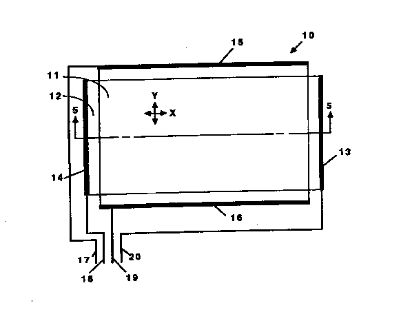
Fig. 1 is a plan view of an analog resistance touch
screen switch of the present invention;
Figs. 2 and 3 are schematic detail diagrams of the touch
screen switch of Fig. 1;
Fig. 4 is a schematic sectional view of the touch screen
switch of Fig. 1;
Fig. 5 is a sectional view in elevation taken in the
plane indicated by line 5--5 in Fig. 1; and
Fig. 6 is a enlarged, elevational view of a portion of
Fig. 5;
Fig. 7 is a fragmentary plan view of a portion of Fig.
6; and
Fig. 8 is a plan view of a second embodiment of the
present invention.
The preferred form of the invention is a switch within a
larger switching device of the type having a construction of
relatively thin or low profile membranes, substrates and
films. Such larger switching devices include transparent
touch panels or touch screens as illustrated in Fig. 1 and 8.
The invention may be applied, however, to other types of
switches. -
Figs. 1-3 shows an analog resistive type of touch screen
10 which includes a top transparent layer 11 disposed over a
bottom transparent layer 12. As seen in detail sketches in
Figs. 2 and 3, the top layer 11 acts as a resistive layer
running in a Y-direction between upper ~us bar 15 and lower bus
2110327
bar 16, and the bottom layer 12 acts as a resistive layer
running in an X-direction between right side bus bar 13 and
left side bus bar 14. As seen in Fig. ~, right side bus bar 13
and left side bus bar 14 are connected to thick film conductors
18 and 20 of silver particle-filled polymer, which in turn
connect to decoding circuitry (not shown) of a type known in
the art. Similarly, upper bus bar 15 and lower bus bar 16 are
connected to the decoding circuitry by thick film conductors 17
and 19 of silver particle-filled polymer.
AS shown in Fig. 4, the analog resistive touch switch 10
is operated by applying a voltage gradient (VIN) across one
conductive layer (the bottom layer 12 in this instance) and
measuring voltage VouT at a point of contact with the opposing
conductive layer 11, which is left floating to sense VouT. The
bottom layer 12 comprises a substrate 21, bus bars 13, 14, and
a transparent resistive coating (shown as two resistors RLEFT
and RRIGHT) connected in series between the two bus bars 13,
14. The point of contact is represented by the vertical arrow
marked VouT. The resistance between the point of contact VouT
and the right bus bar 13 is represented by RRIG~T~ and the
resistance between the point of contact VouT and the left bus
bar 14 is represented b~ RLEFT. The ratio of voltage measured
between the point of contact and the grounded bus bar 13 to the
voltage gradient (VIN) is equal to the ratio of the resistance,
RRIGHT, to the total resistance RRIGHT + RLEFT. Thus, the
touch switch acts as a voltage divider circuit. By alternately
applying the voltage gradient ~one bus bar at VIN, the opposite
bus bar grounded) in the X-direction, and later in the Y-
direction, and using Vo~T valves, the x-Y coordinates of the
touch can be determined by the decoding circuitry.
--6--
2110327
AS shown in Figs. 2 and 3, the conductive layers 11 and
12 can be represented as a group of resistive elements which
are connected in parallel. They further illustrate, that the
total resistance in the X-direction between the bus bars 13,
14, is the same, without regard to the Y-coordinate along the
bus bars 13, 14. Also, the total resistance in the Y-
direction between th~ bus bars 15, 16 is the same, without
regard to the X-coordinate along bus bars 15, 16.
Referring to Fig. 5, in which the thickness is
exaggerated and not to scale, the bottom layer 12 of the
touch panel 10 includes a substrate 21 of polyester. The
substrate 21 is flexible, but could also be rigid. Other
suitable materials for the substrate 21 include glass. A
thin film of indium tin oxide (ITO) is sputtered on the
substrate 21 to form a rectangular-shaped conductive element
22 of from 60 to 500 ohms per square over the top surface of
the substrate 21. Thus, far the bottom layer 12 is of a type
known in the art. The ITO is a semiconductive ceramic with
excellent transparency and light transmitting
characteristics. Tin oxide can also be used for the
conductive layer 22. The top layer 11 includes a flexible
sheet of polyester 23. A thin film of indium tin oxide (ITO)
is sputtered on one side, which becomes the underside of the
top layer 11, to form a rectangular-shaped conductive element
24 opposing conductive element 22. Thus, far the top layer
is of a type known in the art.
Continuing with the description relative to Fig. 5, a
spacer of adhesive 25 is formed in a rectangular pattern with
a central opening between the top and bottom layers 11, 12.
The width of the switch is not to scale relative to the
211~327
thickness in Fig. 5, so that both left and right sides of
adhesive perimeter 25 can be seen in Fig. 5. Bus bars 13,
14, 15, 16 of silver particle-filled polymer thick film
conductive ink, usually about 1000 times more conductive than
the ITO layers, are formed along the edges of layers 11, 12
as seen in Fig. 1. BUS bars 13 and 14 contact the layer 26,
which contacts layer 24, as seen in Fig. 5. sus bars 15 and
16 contact layer 27, which contacts layer 22, as seen in Fig.
5.
The invention provides an additional, very thin film of
palladium 26 which is coated over the ITO layer 24. This
film may be in the range from about 5A to about 70A thick.
In the preferred embodiment, the film is coated at a
thickness of about lOA to about 30A, these thicknesses being
difficult to measure. Also, in the preferred embodiment, a
second film 27 of palladium is coated on the bottom ITO layer
22. At this thickness, the metal film probably forms islands
27a, as shown in Figs. 6 and 7, rather than a continuous
film. Therefore, sheet resistance is still controlled by the
ITO layers 22, 24. optical absorption is very low and light
transmission ~ualities are decreased by about 1% to 4%, which
is not considered significant.
Contact resistance, which is a surface phenomenon, has
been measured with the loA-30A thickness of palladium film,
as described above, on top of ITO. The contact resistance
was much lower than ITO alone at the beginning of the test,
increased only slightly during switch closure cycling tests
and generally provided much more consistent performance than
ITO without such a film.
In one test, a palladium film of lOA-30A thickness, as
--8--
2110327
described above, was deposited onto touch panel material that
was made of the standard high resistance ~300 to 500
ohm/square~ ITO film, and was assembled into a test switch.
This test switch, along with a switch made from the identical
film with no palladium, were actuated in an identical
fashion. The actuator dropped a sine-wave driven weight of
about 150 grams onto a single spot on the switch three times
per second. The tip of the actuator was a 0.5-inch diameter
silicone rubber hemisphere. The switches were unpowered and
the contact resistance was measured at intervals up to
1,000,000 actuations and more, for the palladium switch. The
non-coated switch exhibited erratic resistance values that
varied as much as +/- 20% even before the actuation test was
begun, whereas the palladium-coated switch varied less than
+/- 1.5%. The initial contact resistance of the palladium-
coated switch was less than hal of the non-coated switch,
which may be significant, although the switch geometry was
not identical. After 1,000,000 actuations, the non-coated
switch showed average contact resistance increases of about
100%, if spurious extremely high readings are ignored,
whereas after 1,500,000 actuations, the palladium film switch
resistance increased only 14%, and had no high resistance
readings.
In a second test, analog resistive touch screens were
tested for actuation life to compare screens made with and
without a thin palladium film on both contacts as described
herein. Tests were performed with a 5/8~ diameter silicone
hemispherical ~fingerU and a 0.06" diameter flat Delrin~
plastic tip. Actuations were at 3HZ with lgO grams of force.
30 The touch screens were powered with conventional 8-bit
2110327
decoding circuitry. The position of the touch was monitored
by a computer every 15 minutes, where an average o~ 30 points
was compared to the initial position. ~ailure and therefore
termination of the test was determined when the measured
position moved 10% of full scale from the initial position.
The test results are presented below. Test results fo~ the
palladium were terminated prior to failure so the data
represents only a minimum of actuation life and the actual
life could be much greater. All numbers are given in
thousands of actuations and represent averages of a number of
test~ excluding the high and low readings.
S~reen Tv~e Sili~Qne Ti~ .~lastic Ti~
Non-Coated 36,000 128,000
Palladium-Coated 835,000 2,066,000
The invention is also illustrated as applicable to a
touch switch of the matrix type seen in Fig. 8. In this
switch 30 a plurality of transparent conductors 31 running in
the Y-direction are formed of thin film ITO material on the
underside of top flex layer (not shown). ~ second plurality
of transparent conductors 32 are formed of ITO material on
the top of substrate (not shown). Bus bars 33 of silver
particle-filled polymer thick film ink connect to the endæ of
the conductors 31. Bus bars 34 of the same material connect
to conductors 32. When the flex layer with conductors 31 is
flexed, contact is made at the intersection of one conductor
31 running in the Y-direction and one conductor 32 running in
the X-direction. Conductive traces 35, 3~ of silver
particle-filled polymer thick film ink co~nect these
conductors 31, 32 to suitable decoding circuitry of a type
-10 -
'~110327
known in the art to determine the ~-Y position of matrix
touch panel activation. The ITO conductive strips 31 and 32
can be coated with a thin film of palladium 27 as shown in
Figs. 6 and 7 to accomplish the same results as discussed
above for the analog resistive touch screen in inhibiting
changes in contact resistance.
This description has been by way of example of how the
invention can be carried out. Those of ordinary skill in the
art will recognize that various details may be modified in
arriving at other detailed embodiments, and that many of
these embodiments will come within the scope of the
invention. Therefore to apprise the public of the scope of
the invention and the embodiments covered by the invention
the following claims are made.
-11-