Note: Descriptions are shown in the official language in which they were submitted.
21 L07~
SEI 93-37
I TITLE OF THE IMVE~TION
~ . . .
Compound Semiconductor Device and Method for
~abricating the Same
BACKGRO~ND OF THE INVENTION
It is disclosed in Yarious references~ e.g. ~ A.
Fiathimulla et al,, "High-Performance InAlAs/InGaAs
~EMT's and MESFET`s", IEEE EL~CTRON DEVICE ~ETTERS, vol.
9, No. 7, July 1988, ps. 328-33n; Shinobu Fujita et al.
"InGaAs/InAlAs HEMT with a Strained InGaP 5chottky
Contact Layer", IEEE ELECTRON DE~ICE LETT~RS, vol. 14,
No. 5, May 1993,ps 259-261; and Ja~anese Patent Laid-Open
Publication No. 160161/1993 that materials lattice-
matched on InP substrates, or materials which do not
lattice-match on InP substrates but are grown in a
thickness below a critical film thickness, which do not
incur, i.e., compounds such as InP, Gal-xAs, etc., are
æuitable to realize high speed high frec~ency
semiconductor devices.
- ~he schematic structure of the ~EMT's disclosed in
these references comprises, as exemplified in Fig. 6, on
a semi-insulatLng InP substrate 1 a non-doped InAlAs
buffer layer 2, an InGaAs channel layer 3, an n-InAlAs
donor supply layer 4, a heavily doped n-type InGaAs cap
layer 5, sourc:e and-drain ohmic electrodes 6, 7 vaporized
on the upper surface of the cap layer 5. ~his structure
further compriscs a Schottky gate electrode 8 vaporized
21~ 0 ~ 9 ~ ;
. SEI 93-37
1 in Schottky junction with the donor supply layer in a
recess structure which is formed:b~ ~tching the cap layer
- 5 down to the donor supply layer 'L.
SUMMARY OF THE I~VENTION
This invention relatQs to a compound semiconductor
device having a structure in which a Schottky gate is
formed on a donor supply layer through a recess
structure. Specifically an object of this invention is
to provide a compound semiconductor device of an
1~ innovational structure which can further improve
characteristics.
To achieve the object, the compound semiconductor
device according to this invention comprises an
insulating film with ~n opening in a portion thereof,
which is formed on a cap layer formed on a donor supply
layer, and a Schottky ga~e elec~rode being in Schottky
junction with the donor supply layer by vacuum
vaporization in a rPcess structure etched wider than an
: open area of the opening, extended upward through the
recess s~ructure and overlapped on an outside periphery
of the opening.
In this structure7 since the r~cess structure has a
wider space in the cap lay~r ~han an open area of the
opening in the insulatîng film, ~acuum spaces between the
cap layer and the side walls of the Schottky gate
~lectrode. Accordingly the Schottky ga~e electrode is
2 ~ -:
` ~107~3
SEI 93-37
1 not in direct Schottky junction with the cap layer and in
Schottky junction only with the donor supply layer. Thus
gates of semico~ductor devices, ~uch as HE~T's and
MESFET's, can be realized. Since the Schottky ga~e
electrode is ovsrlapped on an out:side peripheral portion
of the opening in the insulating film, the spaces in the
recess struc~ure can be tightly shielded from the outside
in a Yacuum condition. As a result, a problem that
impurities intrude into a portion of th~ donor supply
layer in the recess structure with a re~ult of
deteriorated electric characteristics can be prevented.
To be specific, in compound semiconductor devices of the
conventional recess structures, since the recess
structures are exposed to ~he outside ambient atmosphere,
portions of the donor supply layers are exposed to the
outside ambient atmosphere. Accordingly in the
semiconductor fabrication processes, the exposed
portions (peripheral portions of the Schottky gate
electrodes~ are oxidized with a result of deteriorated
elec~ric characteristics. But the recess structure ~.
according to this invention never incurs such problem.
This inven~ion is widely applic~ble to various -
compound semiconductor devices, such as ~EMT's and
MESP~Tis with:recess structures for Schottky gate
leckrodes. The recess structure accordiny to this
invention is not limited to applications in specific . . .
"~"":",~
2 ~ 7 9 1j
SEI 93-37
1 compound semiconductors but is widely applicable to
oompound semiconductor devices formed of various compound
semiconductors. The forma~ion of the recess structure
according to this invention does not need complicated and
specific fabrication steps. and accordingly this
invention can be eiasily practiced. Thus this invention
can produce excellent advantageous effects.
The present invention will become more fully
understood rom the detailed description given
hereinbelow and the accompanying drawings whiGh are given
by way of illus~ration only, and thus are not to be
considered as limiting the present invention.
Further scope of applicability of the present
invention will become apparent from the detailed
description given hereinaf~er. ~owever, it should be
understood that khe detailed description and specific
e~mples, while indioating preferred ~mbodiments of the
invention, ara given by way of illustration only, since
various changes and modifications within the spirit and
scope of the in~ention will become apparent to those
skilled in the art form this detailed description.
BRIEF DESCRIPTIC)N OF THE DRAWINGS
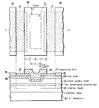
Fig~ 1 is a pl~n layout view and vertical s~ctional
view of the co~pound semiconductor device according to a
~irst embodiment of this invention;
Figs, 2A to 2D are vertical sectional views of the
21~7~
SEI 93-37
compound semiconductor device according to the first
embodiment in the respective steps of its fabrication
process;
Fig. 3 is a vertical sectional view of the
modification of the first embodim~nt shown in Figs. 2A to
2D;
Fig. 4 i~ a vertical sectional view of the compound
semiconductor device according to a second embodiment of
this invention;
Fig. 5 is a vertical seckional view o~ the compound
semiconductor device according to a third embodimen$ of
this in~ention; and
Fig. 5 is a vertical sectional view of a
conventional compound semiconduc~or device.
DESCRIPTION OF THE PREFERRED EMBODIMENT
.
Embodiment 1
.
A HEMT as the compound semiconduc~or device :-
~ccording to a firs~ embodimen~ of ~his in~ention will be
e2plained with reference to Figs. 1 and 2~ to 2D. Fig. 1
: 20 is a plan view ~upper drawing) of a major portion of the
HEMT, and a vertical sectional view (lower drawing~ along ~:
. .
the phantom line L-L in Fig. 1. Figs. 2A to 2D are views -
of the steps o:E the HEMT fabrication.
The structure of the major portion will be explained ~ .
with reference to Fig. 1. On a semi-insulating InP
~ubstrate 10 there are for~ed buffer layer ll'of undoped
-~:
" '. ~ `:
:"'',','''
-- _ 2 ~ o r~
SEI 93-37
1 InP or InAlAs which is lattice-matches with InP, an
InGaAs channel layer 1?, an n-type InAlAs donor supply
layer 13, and a heavily doped n-type InGaAs cap layer 14
in the stated order. Further a d:rain and a sourse ohmic
electrodes 15, 16 are vaporized on set regions on the cap
layer 14, and heavily doped n type layers (the regions
indicated by the dot lines in Fig. 1) are formed below the
ohmic electrode~ lS and 16 by alloying.
An insulating film 17 of SiN i8 formed on a rest
portion of the cap layer 14 except regions wi~h the ohmic
electrodes 15, 16 formed on, and a region with a Schottky
gate electrode 18 formed in (a region for an opening P1
which will b~ explained later). In the region with the
Scho~tky gate electrode in (a r~gion between the drain
and source) there is formed, bec~use of the partial
absence of ~he insulating film 17, a rectangular opening
P1, and a recess ~ructure which corresponds to the
opening P1 and arrives down at a par~ion of an upper
portisn of the donor supply layer 13 through the cap layer
14. In the rece~s structure the Schottky electrode 18
which is in Schottky junction with the donor supply layer
13 i~ vacuum vapori~ed. -
The Schottky electrode 18 partially contac~s with -
the donor supply layer 13 and is extended without contact
with the cap layer 14 upward through the opening P1 to
overlap portions of the upper surface of the insulating
2~1~)7~3~
- SEI 93-37
1 ~ilm 17 outside the opening P1.
Then, an example of the fabr.i~ation process of the
HEMT havlng such structure will be explained, referriny
to Figs. 2A-2D. In the ~irs~ step o$ the process shown in
FigO 2A, ~he ~uffer layer 11 formed of undoped InP or
InAlAs which is lattice-ma~-ched with InP, is deposited on
the su~strate 10 formed of semi-insulating InP with about
3000 A thickness by Molecular Beam Epitaxy method ~MBE)
or Organic Metallic Vapor Phase Epitaxy method (OMVPE).
~ext a channel layer 12 formed of InGa~s i~ deposited on
the buffer layer 11 with ~bout 150 A thickness. Fur~her,
the doner supply layer 13 formed of In~s2Al0~8As having a
electron concentration of SxlOl~/cm3 is deposited on the ~ ~ -
channel layer 12 with about 400 A thickness. The cap
layer 14 formed of InO 63Ga047As having an electron ~ :
concentration of 5~1018/cm3 iS formed on the doner supply
layer 13 with about 100 A thickness. The material of the
channel layer may be InP.
Next, in ~he second step shown in Fig. 2B, the drain
2~ and source ohmic elec~rodes 15 and 16 are evaporated on a `.
pred~termined area of the cap layer 14 and the high
- d~nsity n ~pe layer i form~d under the ohmic electrodes
15 and 16 by alloy process. Next, the insulating layer 17 -~.
: .~osmed o$ Si~ i~ formed with about 500 A - lG00 A ~.
thickness. Although such SiN insulating layer can be ::
formed a~ rela~ively low temperature, an insula~ing
7 -:~
---~ 2110 19 ~3
. SEI 93-37
1 material e.g., SiO2 or SiON which can be formed at
temperature lower than that of SiN may be used.
Next, in the third step sho~m in Fig. ~C, a portion
of the insulating film 17 for the opening P1 to be formed
therein is removed uæing a photoresis FA by the known
. photnlithographyO That i~, the opening P1 is the mask for
the recess etching, which will be explained later and
defines a channel length and width of the gate. After the
opening P1 i~ formed the photoresist FA is removed.
Next, in the fourth s~ep shown in Fig. 2D, a
photoresist FB is formed again by the known
photolithography on a rest region other than a region Q1 ;-~
including the opening P1. As shown in Fig. 1, the region
Q1 is largar than the opening each by 0.5 ~m in the
direction of length of the gate and each by 1.0 ~m in ~he
direction of width of the gate. Thus, after the
pho~or~sist FB is formedO tha cap layer is recess-etched
down to the donor supply layer 13 wi~h the insula~ing film
17 and the photoresi~t FB as ~he mask. .;
2~ I~ the recess etching, aqueous phosphoric acid
solution and hydrogen peroxide solution are used a~
etchant. This recess etching forms, as shown, the reces~
~tructure corresponding to the opening P1 as shown in
Fig. 2D, and the cap layer 14 is etched more widthwise
than the openi:ng P1 of the insulating film 170
Accordingly the space ~ormed in the cap layer'14 by this
.
. 2 L107~:3
- S~I 93-37
1 recess structure is wider than the opening Pl of the
insulating film 17.
Then, Ti/Pt/Au are vacuum vaporized sequentially in
reæpective 500 A/500 A/sooo A thi.cknesses so as to cover
the opening P1 and the region Q1. Then an unnecessary
portion of the photoresi~t FB is lift~d off to form the
Schottky gat~ electrode 18 as shown in ~ig. 1. Since this
vacuum vaporization forms the Schottky gate electrode 18
in a rectangular sectional shape contour to the opening ;~
P1 in the insulating film 17, the Schottky gate electrode
18 is in contact with the donor supply l~yer 13 but out of : :
contact with the cap layer 1~ which is etched up to
portions inner of the opening P1. Since the unnecessary
photoresist FB has been lifted OffJ the Schottky
electrode 18 i5 vaporized onto the region Q1 partially on
the upper surface of the insulating film 17. Thus the ~ :
opening P1 is tightly closed by the overlapping Schottky
gate electrode 18 on the portion of the insulating film
17! and an interior space of the recess structure is :
perfectly shielded from outside ambient a~mosphere.
Thus, in the firs~ emhodiment, as shown in Fig. 1,
the Schottky electrode 18 covers a portion of the
insulating film 17 and contacts with the donor supply
layer 13. Accordingly the Schottky electrode 18 itself
can shield the recess structure from the outside to
thereby expel causes for deterioration of electric
211~ 19 1~
. SEI 93-37
1 characteristics, ~uch as oxidation of the donor supply
layer 13. in~rusion of impurities, etc. For example, the
InAlAs donor supply layer containing Al (aluminum) is so
active ~hat the formatio~ of the ';chottky electrode
directly on the donor supply laye:r by the conventional
methods easily causes sxidation with a result o~
deterioration of electric characteristics, such as
decrea~es of drain current, but the first embodiment can
solve such problem.
In the fourth step shown in Fig. 2D, the aqueous
phosphoric acid solution and the hydrogen pero~ide are
u~ed as etcha~t to form the recess structure having a
tapered side wall as shown in Fig. 1. But, in the fourth
step, etching gas with CH4+H2 , ins~ead of the above
etchant, can be used to form ~h~ recess structure. The ~:~
application of the etching gas with CH4+Hg , as shown in
Fig. 3, realizes the formation of a r~cess structure
having ~ side wall ~ubstantially perpendicular to the
laminated surf~ce of the insulating layer 17 on the donor
supplying layer 13 and ~he cap layer 14 at the position
inside from an edge of the opening P1 of the insulating
layar 17. By making the side wall of the recess structure
to be substantially perpendicular to the laminated
surace of ~he insulating layer 17, the side wall is
surely spaced from the Scho~ky electrode 18 so that the
interior space of the recess structure is per~ectly
: `-` 2:L~I: 7~1~
SEI 93-37
1 shielded from out~iide ambient atmosphere.
In the first embodiment, the Schottky electrode 18
has been explained in terms o the prev~ntion of
oxidation and intrusion of im~urities in connection with
the vicinity of the portion wherle the Schottky electrode
is formed on and the donor supply layer 13 in the recess -~
qtructure. Further, this embodiment is effective to the
prevention of oxidation of the Schottky electrode 18 ~ :
itself.
The first embodiment has been explained by means of .
a HEMT, but is not limit~d to ~ESF~T's and other compound -~
semiconductor devices which have recess structures.
Further, the above can be applied to a compound
semiconductor device except for a semiconductor device
having an InP ~ubstra~e, for examplet a semiconductor
device having a G~s substrate.
Embodiment 2
A second embodim~nt of this invention will be
explained with r~ference to Fig. 4. Fig. 4 is a vertical
sectional view of a major portion of ~he ~EMT according to
the second embodiment.
First, khe structure o~ the HÆMT will be e~plained.
An undoped GaAs bu~fer layer 21 i~ formed in 3000 A on a
GaAs sub~tra~e 20. On the buffer layer 21 a donor supply
layer 22 of GaO7Alo~As of a 1~10l8/cm3 electron
concentration is formed in 500 A. On the donor supply
11
21~ 3~
. SEI 93-37
1 layer 22 a Ga~s cap layer 23 of a 5zlOla/cm3 electron
concen~ration i~ formed in 500 A. Drain and source ohmic
electro~es 24, 25 are vaporized on set regions on the cap
layer 23, and a heavily doped n-t:ype layer (indicated by
the dot ~ine~ in Fig, 4) are formed by alloying below the
ohmicielectrodes 24, 25.
An insulating ~ilm 26 of ælN ls formed in a thickne~s
o about 500 A - 1000 A on the ohmic electrodes 24j 25,
and on a rest portion of the cap layer 23 other than a set
region thereof for a Schottky electrode 27 to be ~ormed
in. In the reglon for the Schottk~ electrode 27 to be
formed in (a r~gion between the drain and the source) the
insulating film 26 is partially ab~ent to define a
rectangular opening P2, and a recess structure
corresponding to ~he opening P2 and e~tended down to a
portio~ of a~ upper portion of the donor supply layer 22
. through the rap layer 23. ~he Schottky electrode 27 is
formed by vacuum vapori~ation in the recess structure in
contact wi~h the donor supply layer 22. The Schot~ky
electrode 27 is formed by vacuum vaporizing Ti/Pt/Au
sequen~ially in resp~ctive 500 AJ500 A/5000 A
thicknesses.
The Schottky electrode 27 partially contacts with
the donor ~upply layer 22, and extended upward through
the opening P2 without contacting the side walls of the
cap layer ~3 to overlap on portions of the upper surfa~e
.
~2
2~079~j :
SEI 93-37
1 of the insulating film 26 outside the opening P2.
This HEMT is fabricated by the following fabrication
prociess. This process will be explained in accordance
with the steps (shown in Figs. 2A to 2D) o~ the
fabrîcation proces~iof ~he first embodimentO In the
first step the buffer layer 21, the donor supply layer 22
and the cap layer Z3 are formed in the stated order on the
GaAis sub~trate 20 by molecul~r beam epitaxy (MBE) or
organometallic vapor phase epitaxy ~OP~PE~.
Next, in the second step, drain and source ohmic
electrodes 24, 25 are ~aporized on set regions on the cap
layer 23, and then a heavily doped n~type layer is formed
below the ohmic electrodes 24, 25 by alloying. Then an
SiN insulating film 26 is formed in an abo~lt 500 A - 1000
A thickness by plasma CVD. This SiN insulating film 26
can be formed at comparatively low temperatures, but
insulating materialis which can be formed at low
temperatures than Si~ e.~., SiO2, SiON, etc., may be
used.
Then, in the third step, a portion of the insulating
:, ~ilm 26 corresponding to the opiening P2 is r~moved using a
: ~hotoresist (corresponding to the photoresist F~ in Fig. -
2C) by the known photolithography. ~hat is, this opening
P2 functions as a mask ~or recess etching, and
substantially defines a channel length and a width o~ a
gateO After the formation of ~he opening P2, ~he
13 ~ ::
21107.'~0 ~;
SEI 93 37
1 photoresist is removed.
Sub~equently, in the fourth step, a photoresist
(corresponding to the photoresist FB in Fig. 2D) is
applied to a rest portion of the insulating film 26 e~cept
a region Q2 which is larger and c:ontains the openiny P2 by
the ~nown photolithography. The formation of th~
photore~ist is followed by recess etching the cap layer
23 down into the donor supply layer 22 with the insulating
film 26 and the photoresist as a mask.
For the rec~ss etchiny an enchant o~ citric acid
aqueous solution and aqueous hydrogen peroxide is used.
This recess etching forms a rece~s struc~ure having the
so-called inversely tapered side walls, which~ as shown
in Fig. 4, a ~pace is transver~ly increased downward
~rom the opening P2. That is, this recess structure makes
a pace in the camp layer 23 transYersely lar~er than the
opening P2 in the insulating ~ilm 26.
Then, Ti/PtJAu are sequentially vacuum vaporized
respecti~ely in 500 A/500 A~sooo A thicknesse~ so as to
oover the op~ning P2 and ~he region Q2, and subsequently
an unnecessary portion of the photoresist i9 lifted off,
whereby the Schottky gate elPctrode 27 as shown in Fig. 3 -
is formed. Since this vacuum vaporization forms the ~
: Schottky electrode 27 in a rectangular sectional shape of ~ :
the opening P2 in ~he insula~ing film 26, the 5chottk~
gate electrode 27 is in contact with the donor`supply
14
~$~ `. d
2 ~
- SEI 93-37
1 layer 22 but ouk of contact with ths cap layer 23, which
is etched wider than the opening P2. The lift-of~ of the
unnecessary portion of the photo:resist permits the
Schottky gate electrode 27 to be vaporized even on the
region Q2 on the upper sur~ace of the insulating ~ilm 26.
Thus, the opening P2 is tightly closed by the overlapping
Schottky gate ele~trode 27 on the upper surface of the
insulating film 26, whereby an interior space of the
recess structure is perfectly shielded from outside
ambient atmosph~re.
According to the second embodiment, as shown ~n Fig.
4, the Schottky gate electrode 27 is formed in contact
with the donor ~upply layer 22 while covering a portion of
the insulating film 26. Accordingly the Schottky gate
electrode 27 itself shields the recess structur~ from the
outsid~ 30 that causes for incurring deterioration of
electric characteristics, such as ogidation o~ thP donor
supply layer 22 an~ intrusion o~ impurities can ~e
expelled.
The second embodiment has been explained by means of ~
HEMT but is not limited to HETMT's. This invention is : ::
applicable to ~ES~T's and other semiconductor devices
having recess structures.
Third Embo~iment
A third e~bodiment of ~his invention will be
explained with reference ~o Fig. 5~ Fig. 5 is a vertical
~5
21 1 0 ~90
. SEI 93-37
1 sec~ional view of a major portion of a HEMT according to
this embodimentO
First, the structure of the HEMT will be explained.
A undoped GaAs buffer layer 31 is formed in a 3000 A on a
GaAs substrate 30. Further a GaO7Alo 3AS donor supply
l~yer 33 of a 5xlOl8/cm~ electronlconcentration is formed
in 400 A, and an InO53GaO47As cap :Layer 34 of a 5xlOla/cm3
electron concentration is formed in 100 A. Drain and
source o~mic electrodes 35~ 36 are formed by vacuum
vaporization on set regions on the cap laver 34. A
heavily doped n-type layer (indicated by the dot lines in
Fig. 5) is formed by alloying below the ohmic electrodes
35, 36.
A SiN insula~ing film 37 i~ for~ed in an about 500
A - 1000 A thickn~s on the ohmic electrodes 35, 36, and
on a rest portion o~ the cap layer 34 other than a region
with a Schottky ~lectrode 38 formed in. The insulating
film 37 is abs~nt in the region with the Schottky ::
electrode formed in (a region ~etween the drain and the
~0 source) to de~ine a rectangular opening P3, and a recess
structure which corresponds to the opening P3 and arri~es
at a portion of an upper portion o the donor supply layer
33 through the cap layer is formed. The 6chottky gate
electrode 3~ is iormed by vacuum vaporization in ~he
recess structure in Schottky junction with the donor
supply layer 33. The Schottky gate electrodei38 is formed
21~37~
5EI 93-37
1 by sequentially vacuum vapori2ing Ti/Pt/Au.
The Schottky gate electrode 38 is in contact only
with the donor supply layer 33~ and extended upward
without contacting ~he side walls of the cap layer 34
through the opening P3 to overlaE~portions of the upper
surface of the insulating film 37.
The HENT of this structure is fabricated by the
following fabrica~ion process. This fabrication process
will be explained in accordance with the steps of the
fabrication process of Figs~ 2A ~o 2D according to the
first embodiment. In the first step, the buffer layer 31,
the channel layer 32 and the donor supply layer 33 and the
cap layer 34 are formed on th~ G~s substrate in the
stated order in the abo~e-described thicknesses by
molecular beam epi~axy (M~E3 and organic metallic vapor
phase epitaxy (O~VPE).
Then, in the second st~p, the drain and source ohmic :~
electrodes 35, 36 are formed by vacuum vaporization on
the set regions, and then the heavily doped n-type layer :-
is formed by alloying below the ohmic electrodes 3S, 36.
The SiN insulating film 37 is formed by plasma CVD in an
about 500 ~ - 1000 A thicknessO The SiN insulating film -
37 can be comparatively low ~emperatures, but it is
- . possible to use an insulating material which can be
formed at a lower temperature than SiN, such a~ SiO2 or
SiON.
17
21~07~10
. SEI 93-37
1 Ne~t, in the third stepi the region of the
in~ulating film 37 for the opening P3 to be formed in is
removed by the known photolithography using a photore~ist
(corresponding to the photoresist FA in Fig. 2C). The
opening P3 functions as a ma~k fo:r the recess etching and
defines a channel length and channel width of a ga~e. The
formation of the ope~ing P3 is followed by removal of the
photoresist.
Then, in the fourth step, a photoresist
(corresponding to the photoresist FB in Fig. 2D3 is ::
applied to a rest portion of tha insulating film 37 except
a region Q3 which is larger and contains the opening P3 by
the known pho~olithography. The formation o~ the
photoresis~ is followed by recess etching the cap layer
34 down into the donor supply layer 33 with the insulaking
~ilm 37 and the photoresist a~ a mask.
For the recess etching an etchant of aqueous
sulfuric acid solution and aque~us hydrogen peroxide is
: used. As shown in Fig. 5, the recess structure
corresponding to the opening P3 is formed in the donor
supply layer 330 and ~he cap layer 34 is etched a little
wider than the opening P3 in the insulating film 37.
Accordingly a ~pace formed by tha recess structure in the
cap layer 34 is wider than the opening P3 in the
insula~ing film 37.
Then, Ti/Pt/Au are se~uentially vacuum v~porized
lfl
21~07 ~3 0
S~I 93-37
1 respectively in 500 A/soO A/sooo A thicknesses so as to
cover the opening P3 and the region Q3, and subsequently
an unnecessary portion of the photoresist is lifted off,
whereby th~ Schottky gate electrode 38 as shown in Pig. 5
is formed. Since this vacuum vapori~ation ~orms the
Schottky electrode 38 in a rectangular æectional shape o~
the opening P3 in the insulating film 37, the Schottky
gate electrode 37 is in contact with the donor supply
layer 33 but out of contact with the cap layer 34, which - .:
~0 is etched wider than the opening P3. The lift-off of the ~ .
unnecessary portion of the photoresist permits the
Schottky gate electrode 38 to be vaporized even on the
region Q3 on the upper surface of the insulating ~ilm 37.
Thus, the opening P3 is tightly closed by the overlapping
Schottky gate electrode 38 on the upper surface of the :~
insulating ~ilm 26, whereby an interior space of the -
: recess struc~ure is perfectly shielded from outside
ambient atmosphere. .
According to the second embodiment, as shown in Fig.
29 5, the Schottky gate electrode 38 is formed in contact
with the donor supply layer 33 while covering a portion of
the insulating film 37. Accordingly the Schottky gate
: electrode 3g itself shields the recess struc~ure from the
outside, so that causes for incurring deterioration of
electric characteristics, sllch as oxidation of the donor
supply layer 33 and intrusion of impurities can be
19
211~ ~ 9 ~3
. SEI 93-37
1 expelled.
The second embodiment has been explained by means of
HEMT but is not limited to HETMT's. This inventio~ is
applicable to MESFET's and other semiconductor devices
having r~cess structures.
From the invention thus described, it will be
obvious that the invention may be varied in many ways~
Such variations are no~ to be regarded as a depart~lre from
the spirit and scope o~ the invention, and all such
modifications as would be obvious to one skilled in the
art are intended to be included within the scope of the
following claims.
;
~; ....
2~
1~ ' .
. 20