Note: Descriptions are shown in the official language in which they were submitted.
DI~ ;~hl.. . lAL AMPLIFIER CIRCUIT
BACKGROUND OF THE lNv~NlIoN
1. Field of the Invention
The present invention relates to a differential amplifier
circuit and more particularly, to a differential amplifier
circuit to be formed on Complementary Metal Oxide SemiconductOr
(CMOS) integrated circuits or on bipolar integrated circuits,
which has an improved transconductance linearity.
2. Description of the Prior Art
Fig. 1 shows an example of conventional differential
amplifier circuits with a CMOS structure whose transconductan~e
'
linearity is improved. '
The differential amplifier circuit shown in Fig. 1 is
composed of a first differential pair of MOS transistors M11 and ~:
M12 which are driven by a constant current source 51 (current:
Io) and a second differential pair of MOS transistors M13 and ~.
M14 which are driven by a constant current source 52 (current: I
aI0, a~1). The transistor M11 has the same ratio (W/L) between ';
its gate length L and gate width W as that of the translstor ~ '
M12, the transistor M13 has the same ratio (W/L) betwe~n its
gate length L and gate width W as that of the transistor M14.
When the transconductance parameters of the transistors M11 and
M12 are ~oth defined as ~, the transconductance parameters of
the transistors M13 and M14 are bp where b~1, respectively. '
The transconductance parameter ~ is expressed as
= ~(Cox/2)~w/L)
(1)
where ~ is the effective surface carrier mobility and COx is a
gate-oxide capacity per unit area.
In Fig. 1, the gates of the transistors M 11 and N14 coupled
together and the gates of the transistors M 12 and M13 coupled
together form differential input ends of the differential
amplifier clrcuit. An input voltage V~, iS applied to the
differential input ends. ~ ;
The drains of the transistors M11 and M13 coupled together
and the drains of the transistors M12 and M14 coupled together
form differential output ends of the differential amplifier
circuit. ~
,. , ,~ ~.
The sources of the transistors M11 and N12 are connected in '~
common to the constant current source 51 and the sources of the
transistors M13 and M14 are connected in common to the constant
current source 52.
~ . ' '''
Assuming that the transistors M11, M12, M13 and M14 are
operating at their saturation regions, drain currents Idll and
Idlz of the tran~istors M11 and M12 are respectively expressed as
the following equations (2-1) and (2-2) using the
transconductance parameter ~, the threshold volta~e V~ of the
transistors M11, M12, M13 and M14 and gate-source voltages VGS11
and VGS12 Of the transistor M11 and M12.
Idll = ~(V~sll ~ V~) (2-1)
It12 = ~ (VGS12 ~ VTH) ( 2-2 )
The drain currents Idll and Idl2 satisfies the relationship as
Idll + Idl2 = Io
Accordingly, the difference of the drain currents Id,l and
Id12 is given as the following equations (3-1),(3-2) and (3-3) .
Idll ~ Id12 = ~ Vin ~(2Io/~) ~ Vl2n (¦Vinl ~ ~ ) (3-1)
Idll - Idl2 = Io ( Vin 2 ~71i) (3-2
Idll - Idl2 = - Io ( Vin ~ -~711) (3-3
, y , i
\
In the equati.ons (3-1), (3-2) and (3-3), the input voltage
V~n satisfies the expression as V1n = V~sl1 - V~s12
Drain currents Id13 and Idl4 of the transistors M13 and M14
can be expressed as equations similar to the equations (2-1) and
(2-2), respectively. Here, the drain currents Id~3 and Id14
satisfies the relationship as Id13 + Id1~ = aIol so that
difference of the drain currents Id13 and Id14 is expressed as the
following equations (4-1),(4-2) and (4-3), where a<(a/b)<1.
Id3 - Id4 = b ~ Vin ~ (2aIO) / (b~) - Vl2n (4-1)
(¦Vinl 5 ~ (aIO)l (h~
Id3 - Id~ = a Io (¦Vinl 2 ~(aIO)/(b~)) (4-2)
.
Id3 - Id~ = ~ a Io (¦Vinl 5 ~ ~ (aIo)l(b~)) (4~3) ~
.' '~ '
The differential output current ~I of the differential
amplifier circuit shown in Fig. 1 is given as the following
equations (5-1), (5-2) and (5-3).
dl + Id4) ~ ( Id2 + Id3)
( Idl ~ Id2) ~ ( Id3 - Id4)
= - ,B Vin [ ~(2Io/~) - Vi2R - b~/(2aIO) / (b~) - Vi2n ] (
(¦Vinl ~ ~(2 aIO) / (b~) )
QI = P Yin ~(2Io) ¦ ~ - Vi2" - a Io sgn ( Vin ) (5-2)
(~(a Io) / (b~ Vinl ~
., ,
~I = ( 1 - a) Io sgn ( Vin)
(I I ~ ) (5-3) :~
,.., .~
. The differential output current ~I shown as the equations
. ::.i''':
(5-1), (5-2) and (5-3) is differentiated by the input voltage i~
' V~n. To make the transconductance substantially constant in the '
; equations (5-1), (5-2) and (5-3), the values of the equation ~ '.
~:~ obtained by the di~ferentiation when Vin = O and ¦ Vln¦ = ~
{(aIO)/(b~)}~/2 are required to be equal to each other. ~ '
~ ~,
Therefore, the following relationship has to be satisfied as
'
1 = (b~b1/2)/al/2 (63
Fig.2 shows the transconductance characteristics of the
~:~ 5
~ '
s- .', ".. .
: ':
:
conventional differential amplifier circuit shown in Fig. 1 with
the constants a and b as parameters. In Fig. 2, it is seen that
the fluctuation of the transconductance is limited to 3 % or
less in the input voltage range of ¦Vlnl<0~7tIo/~)l/2~
Fig. 3 shows another example of the conventional
differential amplifier circuits whose transconductance is good
in linearity, which is disclosed by A. Nedungadi and T. R.
Viswanathan in IEEE TRANSACTIONS ON CIRCUITS AND SYSTEMS, Vol.
CAS-31, No.10, pp. 891-894, October 1984, entitled "Design of
Linear CMOS transcon~uctance Elements".
In this paper, they supposed that when the gate lengths of
two MOS transistors forming each unbalanced differential pair
were equal to each other, the differential amplifier circuit
which are composed of two of the unbalanced differential pairs
whose output ends are cross-coupled would have improved
linearity of the transconductance if a ratio of the gate widths
of the MOS transistors forming each unbalanced differential pair
were larger. Then, they obtained a conclusion through the SPICE
simulation in which the ratio of the gate wldths are 10 and 20
that the ratio of the gate widths was required to be 10 or more.
Additionally, they thought that the above-mentioned
conclusion is not practical since such a large ratio as 10 or
~ ;
~:
more leads to a large chip area. Therefore, they proposed the
differential amplifier circuit shown in Fig. 3.
In Fig. 3, there is provided a "Cross-Coupled ~uad cell"
formed of MOS transistors M21, M22, M23 and M24 as a squaring
circuit thereby to improve the transconductance linearity of a
balanced differential pair formed of MOS transistors M26 and M27
having the same gate-width to gate-length ratio (W/L). ;~
The MOS transistors M21 and M22 compose a first differential ;
pair and the MOS transistors M23 and M24 compose a second
differential pair. The first differential pair is driven by a
constant current source 61 which is connected to the common-
connected sources of the transistors M21 and M22 and generates
a constant current (n+l)I. The second dif~erential pair is
driven by a constant current source 62 which is connected to the
co ~n-connected sources of the transistors M23 and M24 and
generates a constant current (n+l)I.
The transconductance parameters of the transistors M21 and
M22 are ko and those of the transistors M23 and M24 are n times
as much as ko~ or nkO. The MOS transistor with the
transconductance parameter nkO is generally realized by n in
number of the unit transistors with the transconductance
parameter ko which are connected in parallel.
The MOS transistors M26 and M27 whose sources are connected
in common at a point B compose a differential pair, which is
driven by a constant current source 63 generating a constant
current aI. The constant current source 63 is connected to the
dif~erential pair at the point B and generates a constant
current aI. The transconductance parameters of the transistors
M26 and M27 are ko.
The gates of the transistors M26, M21 and M23 are coupled
together to be applied with a first input voltage V1. The gates
of the transistors M27, M22 and M24 are coupled together to be
applied with a second input voltage V2.
The drains of the transistors M23 and M24 are connected in
c~ -n to a voltage source (voltage: V~). The drains of the
transistors M21 and M22 are coupled together at a point A, and
between the drains thus coupled together and the voltage source,
there is provided with a constant current source 64 which
generates a constant current aI. An MOS transistor 25 whose
drain and gate are connected to each other is provided between
the points A and B. The transistor M25 serves as a current
level shifter for shifting the current level at the point A to
that at the point B.
MOS transistors M28 and M29 compose a current mirror circuit
,~.,.
serving as an active load of the differential amplifier circuit.
An output current i of the differential amplifier circuit is
derived from the drain of the transistor M29.
In the conventional differential amplifier circuit shown in
Fig. 3, in the range of IxlS(n+1)l/2 where Vl - V2 = v and x =
v/(I/ko)l/2, the drain current ID21~ ID22' ID23 and ID24 of the
transistors M21, M22, M23 and M24 are expressed as the following ~
equations (7-1), (7-2), (7-3) and (7-4), respectively. ' '
ID2l=I[1+~x2+(a/2)x(1_~x2)l/2] (7-1)
ID22=I[l+yx2+(a/2)x(l-~x2)l/2] (7-1)
ID29=I[n-yx2+(a/2)~(1-~x2)1/2] (7-3)
ID24=I[n-yx2+(~/2)x(l-~x2)l/2]
, ~
In the equations (7-1), (7-2), (7-3) and (7-4), a, ~ and
are defined as the following expressions (8-1), (8-2) and (8-3),
~:: respectively. '~
'~'.'.
a=4n/(n+1) (~-1) '
~=n/(n+1)3 ~-2) ~ :
y=n(n-1)/(n+1)3 (8-3)
9 '.~' , "
''~
"'" '"'
The drain current ID21~ ID22 ~ ID29 and ID24 and the constan
currents (n+l)I of the current sources 61 and 62 satisfy the ':~
following relacionship as :.
ID21 + ID24 = ID22 + ID23 = (n+1)I (9)
Accordingly, the sum ( ID21 + IDa2) of the drain currents IDal
and ID22 can be expressed as the following equation (10) and the
drain currents ID25 Of the transistor M25 can be expressed as the
following equation (11).
.
ID21 + ID22 = 2I[1+~YX2~ = 2I + {2n(n-1)/(n+1)2}IX2 (10)
ID25 = aI - (ID21 + ID22) (11)
' ~';'~
Here, the current of the balanced differential pair of the
transistors M26 and M27 is defined as Io~ then the output
current is expressed as the following equation (12).
'
= IDB - ID7 = k V {2Io/k ) - V2}~/2 (IvlS(Io/k )/) (12)
The current Io satisfies the relationship as
.
Io= aI -- ID6 = ID1 + ID2
= 2I + [{2Kn(n-l)}/(n+1)2]v2 (13)
Thus, if the equation (13) is substituted into the equation
(12), the output current i can be expressed as
.
i = k/ v 4I + t 2n ( n - 1 ) ko } 2 (14) i~
~ k ( n + 1 )2 k/ ~:
If the relationship between ko and k' is selected as the
following expression (15), the output current i is obtained as
the following equation (16j.
k' = {2n(n-1)/(n+1)2}kO (15)
i = 2V ~ ~"
2~2n(n-1)Iko (16) ~
n t
,;,~ '';
It is seen from the equation (16) that the differential
amplifier circuit shown in Fig. 3 has a very good ' -
transconductance linearity. -~
Fig. 4 shows still another example of the conventional
differential amplifier circuits to be formed on bipolar
.~
11 ~,
~, '''"' ~':,
integrated circuits, which is disclosed by M. Koyama, H.
Tanimoto and S. Mizoguchi in IEEE 1g89 Custom Integrated
Circuits Conference, pp. 25.2.1 - 25.2.4, entitled "10.7 MHz
Continuous-Time R~n~ra~s filter Bipolar IC".
In Fig. 4, bipolar transistors Q11 and Q12 compose a first
differential pair which is driven by a constant current source
71 (current: Io)~ Emitters of the transistors Q11 and Q12 are
connected in cc ~n to the current source 71. Bipolar
transistors Q13 and Q14 compose a second differential pair which
is driven by a constant current source 72 (current: Io)~
Emitters of the transistors Q13 and Q14 are connected in co ~n
to the current source 72.
Collectors of the transistors Q11 and Q13 coupled together
and collectors of the transistors Q12 and Q14 coupled together
form dif~erential output ends of the differential amplifier
circuit. Bases of the transistors Q11 and Q12 form differential
input ends of the differential amplifier circuit to be applied
with an input voltage Vin.
A direct current (DC) voltage source 73 (Voltage: Vk) is
provided between the bases of the transistors Q11 and Q13 and
a DC voltage source 74 (Voltage: V~j is provided between ~he
bases of the transistors Q14 and Q12. Thus, bias voltages Vk
12
." :'' , - . ' ' ' ' ' : . . ' : : ': ',:,, -
: . , .: ~ : :' ': . ' - . . , , , : . . . ' . :, ',, :
are respectively applied to the bases of the transistors Q12 and
Q13 with their negative ends at the bases of the transistors Q11
and Q14.
An electric current (emitter current) IE Of a p-n junction
diode forming a bipolar transistor can be expressed by the
following equation (17), where I~ is the saturation current, k~
lS Boltzmann's constant, q is the unit electron charge, VBE is
a base-to-emitter voltage of the transistor and T is absolute
temperature.
IE = IS [eXP{(qVBE)/(kBT)} 1] (17)
Here, if the thermal voltage VT is defined as VT = kT/q, as ~ ;
V~ ~ VT~ when exp(V~E/VT) ~1 in the equation (17), the emitter ': j
current IE can be approximated as follows; ~
IE ~ IS eXP(VBE/VT) (18) ;:
As a result, collector currents Icll and Icl2 ~f the ~
transistors Q11 and Q12 can be obtained as follows: ~ .
Base-to-emitter voltages of the transistors Q11 and Q12 are ~ '~
expressed as
. ~
13 ~ ~
.. . . .. ... .... . .. .
V8E11 = VT 1n(IC11/IS) (19--1)
and
VBE12 VT ln(Icl2/Is) (19-2)
Here, the difference between the voltages VBE11 and VBE12 is
defined as V1~ or VBE11_ VBE12 = V1- Then, the sum of the collector
currents IC11 and IC12 is expressed as IC11 + Ic12 = aFIEwhere aF is
the DC common-base current gain factor. Therefore, the
,
collector currents IC11 and IC12 can be given as the following
equations (20-1) and (20-2), respectively. ~ ;
IC11=( aF I0)/{l+exp( V1/VT)} ( 20
Icl2=(,aF Io)/{l+exp (V1/VT)} (20-2)
From the equations (20-1) and (20-2), the difference
between the collector currents Ic1l and IC12 is given as
~ '~
~I1 = IC11 IC12 = aF IO tanh{V1/(2VT)} (21) :'
;'. ''.
The transco~ ctance G~l is expressed by differentiating the
difference QI1 by the voltage V1 as the following equation (22).
: .
Gd = d(~I1)/dVI = {(aFIO)/(2VT)}[1/{COSh (V1/(2VT))}] (22)
\
In the equation (22), the difference V~between the base-to-
emitter voltages V8E11 and V~12 is defined as V1= Vin - Vk where Vk
is the offset bias voltage described above.
With the second differential pair of the transistors Q13 and
Q14, similarly, the difference ~I2 between the collector
currents Ic13 and ICl4 of the transistors Q13 and Q14 can be
expressed as the following equation ( 23 ) . :
~;;
QI2 = IC13 ~ IC14 = aF Io tanh{v2/( 2VT) } ( 23 ) ~ ;:
In the equation ~23), the difference V2 between the base-to- ~ ;
emitter voltages VBE13 and V~14 is defined as V2 = VLn - Vk~ SO that . ~ .
the sum ~I of the current di~ferences ~Il and ~I2 can be given
by the following equation ( 24 ) .
I1 + ~Iz
= aFIO [tanh{ (Vln ~ Vk)/( 2VT)} + tanh{(V1n+ V~)/( 2VT)}] ( 24)
: ,~'' ~ ,;' ',
The sum G~ of the transconductances G~l and Gm2 of the first ! ~ . ,'.
and second differential pairs can be given by the following
equation ( 2 5 ) .
G~ = Gml + Gm2
,
,~ = d(~ )/dvin + d(~I2)/dVln
' ={(aFIO)/(2Vr)} X
~[l/cosh2{(V~ Vk)/(2VT)}] + [l/cosh2{(Vln + V")/(2VT)}]~
(25) '
The transconductance GQ1 in the equation t22) shows the
~ lly flat characteristic when VK= 1.3137 VT. Fig. 5 shows
the transconductance characteristics of the differential
ampliEier circuit. It is seen from Fig. 5 that the fluctuation
of the transconductance is limited to -1 % or less when IV
VT ~
The conventional differential amplifièr circuits described
above have the following problems. With the differential
amplifier circuit shown in Fig. 1, since the circuit has the
transconductance fluctuation about 3 ~, it cannot be employed
.;
to applicatlons requiring the fluctuation less than 3 %, which
means that application fields of the circuit is narrow. In
addition, since the differential output current is e~pressed as
,
the difference between the drain current difference, the current
efficiency with respect to the driving currents is lowO ~'~
With the conventional differential amplifier circuit shown
ln Fig. 3, the differential pair composing the squaring circuit
16
;l ~
is realized by an MOS transistor with the transconductance
parameter ko and n in number of the MOS transistors with the
transconductance parameter ko which are connected in parallel.
Therefore, the chip occupation area is expanded and the current
consumption increases due to a large number of elements.
For example, choosing k = ko/2 in the equation (15), we get
n = 1 + 2/3l/2 . 2.155. Therefore, to obtain a very good
transconductance linearity, each of the unbalanced differential
pairs must be composed of 431 in number of unit transistors and
200 in number of the unit transistors, which requires a very
large chip occupation area. Thus, the conventional differential
amplifier circuit shown in Fig. 3 is not practical.
With the differential amplifier clrcuit shown in Fig. 4, the
input voltage range is not wide to be satisfied.
,
SUMMA~Y OF THE lNv~NlION
Accordingly, an object of the present invention is to
provide a differential amplifier circuit in which an improved
transconductance linearity can be obtained and its circuit
configuration is simple without enlarging its circuit scale.
Another object of the present invention is to provide a
differential amplifier circuit in which the current efficiency
17
can be improved.
Still another object of the present invention is to provide
a differential amplifier circuit which has a substantially
linear transcon~uctance in-a wider range than the conventional
one.
A differential amplifier circuit according to a first aspect
of the present invention includes a first differential pair
formed of first and second transistors, a second differential
pair formed of third and fourth transistors, a third
differential pair formed of fifth and sixth transistors and a
fourth differential pair formed of seve~th and eighth
transistors.
A ratio (W/L) of a gate-width W and a gate-length L of the
second transistor is Kl times as much as that of the first
transistor where Kl ~ 1, a ratio (W/L) of the thlrd transistor
is K2 times as much as that of the fourth transistor where K2 ~
1, a ratio (W/L) of the sixth transistor is K3 times as much as
that of the fifth transistor where K3 ~ 1, and a ratio (W/L) of
the seventh transistor is K4 times as much as that of the eighth
transistor where K
Gates of the first and third transistors and gates of the
..
fifth and seventh transistors are coupled together to form one
18
of differential input ends, and gates of the second and fourth
transistors and gates of the sixth and eighth transistors are
coupled together to form the other of the differential input
ends.
Drains of the first and fourth transistors and drains of the
sixth and seventh transistors are coupled together to form one
of differential output ends, and drains of the second and third
transistors and drains of the fifth and eighth transistors are
coupled together to form the other of the differential output
ends.
Additionally, the differential amplifier circuit of the
first aspect satisfies one of the following conditions ~a), (b)
and (c).
ta) At least one of the ratios (W/L) of the fifth and eighth
transistors is different from at least one of the ratios (W/L)
of the first and fourth transistors.
(b) At least one of K3 and K4 of the third and fourth
differential pairs is different from at least one of K~ and K2
of the first and second differential pairs.
(c) Current values of the first and second constant current
sources are different from those of the third and fourth
constant current sources. ~
19 :'
With the differential amplifier circuit of the first aspect,
there are provided with the first, second, third and fourth
"unbalanced" differential pairs whose ratios (W/L) are each
different from each other. The drains of the first and fourth
transistors whose relative ratios of (W/L) are 1 and the drains
of the sixth and seventh transistors whose relative ratios of
(W/L) is K3 and K4 are coupled together to form one of the
differential output ends. The drains of the second and third
transistors whose relative ratio of (W/L) is Kl and K2 and the
drains of the fifth and eighth transistors whose relative ratios
of (W/L) are 1 are coupled together to form the other of the
differential output ends.
Therefore,: the transcon~uctance linearity of the
differential amplifier circuit can be improved as well as the
current efficiency thereof can be increased.
A differential amplifier circuit according to a second
aspect of the present invention includes a first differential
pair of firs~t and second transistors, a second differential pair
of third and fourth transistors and a third differential pair ~
of fifth and sixth transistors. ~;
The first and second differential pairs are driven by
constant currents whose values are equal to each other, and the
.
~ '
third differential pair is driven by a constant current whose
value is different from those of the first and second
differential pairs. The transistors forming each differential
pair have the same ratios (W/L) with each other.
Gates of the first and third transistors coupled together
and gates of the second and fourth transistors coupled together
form differential input ends. Drains of the first, third and
sixth transistors coupled together and drains of the second,
fourth and fifth transistors coupled together form differential
output ends.
A first DC voltage is applied across the gates of the first
and thlrd transistors and a second DC voltage is applied across
the gates of the second and fourth transistors.
With the differential amplifier circuit of the second
aspect, there are provided with the first and second "balanced"
differential pairs whose ratios (W/L) are each equal to each
other, which are driven by the currents havi~g the same current
values. There is provided with the third "balanced"
differential pair driven by the current different in current
value from the first and second differential pairs. The output
ends of the first and second differentiaI pairs are cross-
coupled. An input voltage is directly applied across the
21
differential input ends of the third differential pair, and the
input voltage is applied across the differential input ends of
the first and stscond differential pairs together with the first
and second DC voltages as offset bias voltages.
Therefore, higher current efficiency than that of the first
aspect can be realized together with the similar
transconductance linearity to that of the prior art.
A differential amplifier circuit according to a third aspect
of the present invention includes a first differential pair of
first and second transistors driven by a first constant current
source, and a second differential pair of third and fourth
transistors driven by a second constant current source whose
current value is equal to that of the first constant current
source.
A ratio (W/L) of the second transistor is K times as much as
that of the first transistor where K ~ 1, a ratio (W/L) of the
~: ,.
fourth transistor is K times as much as that of the third
! transistor. The relative ratio K is 9.5.
Gates of the first and fourth transistors coupled together
and gates of the second and third transistors coupled together
form differential input ends. Drains of the first and third
transistors coupled together and drains of the second and fourth
22
transistors coupled together form differential output ends.
Preferably, the gate-langths of the first and third
transistors are equal to each other.
With the differential amplifier circuit of the third aspect,
there are provided with the first and second "unbalanced"
differential pairs whose ratios (W/L) are each different from
each other. The Drains of the first and third transistors whose
relative ratios are 1 are coupled together and the drains of the
second and fourth transistors whose relative ratios are K (=
9.5) are coupled together to form the differential output ends.
The gates of the first and fourth transistors whose relative
ratios are 1 and K (= 9.5) are coupled together and the gates of
the second and third transistors whose relative ratlos are K (=
9.5) and 1 are coupled together to form the differential input ~ ~
ends. ~'.
Accordingly, the size of the transistor having the larger
. . ,
ratio (W/L) of each differential pair can be restricted to
several times as much as that of the transistor having the
smaller ratio (W/L) thereof. As a result, the circuit scale can
be reduced.
A transconductance with comparatively good linearity can be
obtained in a wider input voltage range.
Z3
' ~
A differential amplifier circuit according to a fourth
aspect of the present invention includes a first differential
pair of first and second transistors, a second differential pair
of third and fourth transistors and a third differential pair
of fifth and sixth transistors.
Bases of the first and fifth transistors coupled together
and bases of the fourth and si~th transistors coupled together
form differential input ends. Collectors of the first, third
and fifth transistors coupled together and drains of the second,
fourth and sixth transistors coupled together form differential ~;
output ends. ;;
--~ A first DC voltage is applied across the bases of the first
and third transistors and a second DC voltage is applied across
the bases of the second and fourth transistors. ~
With the differential amplifier circuit of the fourth ;
aspect, the input voltage is applied across the input ends of
the first differential pair together with the second DC voltages
as an offset bias voltage, the input voltage is applied across
the input ends of the second differential pair together with the
first DC voltages as an offset bias voltage, and the input
voltage is applied directly across the input ends of the third
differential pair.
24
Therefore, an improved transconductance linearity can be
obtained and as a result, the input voltage range can be
~rr~nd~d -
Additionally, improved high-frequency characteristics can
be given since each differential pair is formed of two minimum
unit transistors.
A differential amplifier circuit according to a fifth aspect
of the present invention includes a first differential pair of
first and second transistors, a second differential pair of
third and fourth transistors, a third differential pair of fifth
and sixth transistors, and a fourth differential pair of seventh
and eighth transistors.
Bases of the first and fifth transistors coupled together
and bases of the fourth and eighth transistors coupled together
form differential input ends. Collectors of the first, third,
fifth and seventh transistors coupled together and collectors
of the second, fourth, sixth and eighth transistors coupled
together form differential output ends.
A first DC voltage is applied across the bases of the first
and third transistors, a second DC voltage is applied across the
bases of said second and fourth transistors, a third DC voltage
'.
is applied across the bases of the fifth and seventh
transistors, and a fourth DC voltage is applied across the bases
of the sixth and eighth transistors.
With the differential amplifier circuit of the fifth aspect,
the input voltage is applied across the input ends of the first
differential pair together with the second DC voltages as an
offset bias voltage, the input voltage is applied across the
input ends of the second differential pair together with the
first DC voltages as an offset bias voltage, the input voltage
is applied across the input ends o~ the thlrd differential pair
together with the fourth DC voltages as an offset bias voltage,
and the input voltage is applied across the input ends of the
fourth differential pair together with the third DC voltages as
an offset bias voltage.
Therefore, similar to the circuit of the fourth aspect, an
improved transconductance linearity can be obtained and as a
result, the input voltage range can be ~p~nded.
Additio4ally, improved high-frequency characteristics can
be given since each differential pair is formed of two m;n;rllr
unit transistors.
BRIEF DESCRIPTION OF THE DRAWINGS
26
-' ~
Fig. 1 is a circuit diagram of a conventional differential
amplifier circuit.
Fig. 2 shows a transconductance characteristic of the
conventional differential amplifier circuit shown in Fig. 1.
Fig. 3 is a circuit diagram of another conventional
differential amplifier circuit.
Fig. 4 is a circuit diagram of still another conventional
differential amplifier circuit.
Fig. 5 shows a transconductance characteristic of the
aonventional differential amplifier circuit shown in Fig. 4.
Fig. 6 is a circuit diagram of a differential amplifier
circuit according to a first embodiment of the present
invention.
Fig. 7 shows a transconductance characteristic of the
differential amplifier circuit shown in Fig. 6. ;~
Fig. 8 is a circuit diagram of a differential amplifier
.
circuit according to a second embodiment of the present
invention.
Fig. 9 shows a transconductance characteristlc of the
differential amplifier circuit shown in Fig. 8.
Fig. 10 is a circuit diagram of a differential amplifier ~
circuit according to a third embodiment. ~ '
27 ~-
Fig. 11 shows an output characteristic of the differential
amplifier circuit shown in Fig. 10.
Fig. 12 shows a transconductance characteristic of the
differential amplifier circuit shown in Fig. 10.
Fig. 13 is a circuit diagram of a differential amplifi~r
circuit according to a fourth embodiment of the present
invention.
Fig. 14 shows a transconductance characteristic of the
differential amplifier circuit shown in Fig. 13 in which V~ =
2.634 VT and (1/a) = (4/3).
, . .
Fig. 15 shows a transconductance characteristic of the
differential amplifier circuit shown in Fig. 13 in which Ve =
2.06344 VT and (1/a) = 1.~5625.
Fig. 16 is a circuit diagram of a differential amplifier
circuit according to a fifth embodiment of the present
inventlon. :'
Fig. 17 shows a transconductance characteristic of the
differential amplifier circuit shown in Fig. 16 in which VB1 = ' ;~.
1.2 VT~ V~2 = 3.834 VT and a = 1.3.
Fig. 18 shows a transconductance characteristic of the ~;
differential amplifier circuit shown in Fig. 16 in which VK1 =
0.70814 VT~ V~2 = 2.59546 VT and (1/a) = 1.82532.
Z8
DETAILED DESCRIPTION OF THE PREFERRED EMBODIMENTS
Preferred embodiments of the present invention will be
described below referring to Figs. 6 to 18.
~First embodiment]
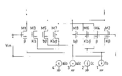
Fig. 6 shows a differential amplifier circuit of a first
embodiment.
In Fig. 6, N-channel MOS transistors Ml and M2 compose a
first differential pair which is driven by a constant current
source 1 whose current value is Io~ N-channel MOS transistors
M3 and M4 compose a second differential pair which is driven by
a constant current source 2 whose current value is Io~ The
first and second differential pairs form a first combined '
differential pair.
N-channel MOS transistors M5 and M6 compose a third
differential pair which is driven by a constant current source
3 whose current value is aI0 where a $ 1. N-channel MOS
transistors M7 and M8 compose a fourth differentlal pair which
is driven by a constant current source 4 whose current value is
:'.
aI0. The third and fourth differential pairs form a second
combined differential pair.
In the first combined differential pair, a ratio (W/L) of
a gate-width W and a gate-length L of the transistor M2 is K
Zg . ~:
times as much as that of the transistor M1 where K ~ 1. A ratio
(W/L) of the transistor ~3 iS K times as much as that of the
transistor M4. The ratios (W/L) of the transistors Ml and M4
are equal to each other.
Gates of the transistor M1 whose relative ratio is 1 and the
transistor M3 whose relative ratio is K are coupled together and
gates of the transistor M4 whose relative ratio is 1 and the
transistor M2 whose relative ratio is K are coupled together.
Drains of the transistors Ml and M4 whose relative ratios are
1 are coupled together and drains of the transistors M2 and M3
whose relative ratios are K are coupled together.
In the second combined differential pair, a ratio (W/L) of
a gate-width W and a gate-length L of the transistor M6 is K'
~times as much as that of the transistor M5 where K' ~ 1. A
'ratio (W/L) of the transistor M7 is K' times as much as that of
the transistor M8. The ratios (W/L) of the transistors M5 and
M8 are equal to each other.
The ratios (W/L) of the transistor M5 and M8 are b times as
much as those of the transistors M1 and M4 where b' ~ 1.
Therefore, the ratios (W/L) of the transistors M6 and M7 are K'b
,~. ....
times as much as those of ~he transistors M1 and M4.
Gates of the transistor M5 whose relative ratio is 1 and the
;~
, ;,
transistor M7 whose relative ratio is K ' are coupled together
and gates of the transistor M8 whose relative ratio is 1 and the
transistor M6 whose relative ratio is K' are coupled together.
Drains of the transistors M5 and M8 whose relative ratios are
1 are coupled together and drains of the transistors M6 and M7
whose relative ratios are K ' are coupled together .
The gates coupled of the transistors Ml and M3 and the gates
coupled of the transistors M5 and M7 are coupled together to
:Eorm one of differential ~ nput ends . The gates coupled of the
transistors M2 and M4 and the gates coupled of the transistors
M6 and M8 are coupled together to form the other of the
dlfferential input ends. An input voltage Vln is applied across
the di.fferential input ends thus formed.
The drains coupled of the transistors Ml and M4 and the
drains coupled of the transistors M6 and M7 are coupled together
to form one of differential output ends. The drains coupled of
the transistors M2 and M3 and the dralns coupled of the
transistors M5 and M8 are coupled together to form the other of
the differential output ends.
In Fig. 6, ~ indicates the transconductance parameters of
the transistors Ml and M4. The transistors Ml to MB have the
transconductance parameters as shown in Fig. 6, respectively.
31
Next, the operation of the differential amplifier circuit
is shown below.
In the ~i~st combined differential pair formed of the
transistors M1 to M4, when gate-to-source voltages of the
transistors M1, M2, M3 and M4 are expressed as V~sl~ Vas2~ Vas3 and ~;
Vqs4 respectively, the threshold voltages of the transistors are
as V~, drain currents Iddl, Id2, Id3 and Id4 of the trans
i
M2, M3 and M4 can be expressed as the following equations (26-
1), (26-2), (26-3) and (26-4), respectively.
"':
. ' ~;
dl = ~ (VGS1_V~) ( 26-1)
Id2 = K~ (VGS2 Y~) ( 26-2)
d3 K~ (VGS3 V~) (26-3)
p
Id4 = ~(Vos~-v~) (26-4) .~: ;
.~, ''~ '.' ','
The drain currents Iddl~ Id2, Id3 and Id4 and the constant '~
currents Io of the current sources 1 and 2 have the following
- . ; ~:
relation~hip (27) and the gate-to-source voltages Vasl~ VaS2~ VGS3 ~'
1: i . I i;~'
and V~34 and the input voltage V~nhave the following relationship
(28). . ~ .
~:
,. i.-
dl + Id2 = Id3 ~ Id4 = Io (27)
32
VGS1 V~S2 VGS4 VGS3 V1n ( 28 )
Therefore, the difference of the drain currents Iddl and Id2
are given as the following expressions (29-1), (29-2) and (29-
; 3), and ~he difference of the drain currents Idd9 and Id4 are
given as the following expressions (30-1), (30-2) and (30-3).
. . .
{ 1 - (l/R) } [{ 1 t (1/~) ] Io ~ 2~Vl2n }
dl d2 { 1 t (~
Vin ( 4/~K) ~{ 1 + (1/~} ( Io/~) ~ Vl2n ( 29-1)
{1 t (1/K)}2
( -~TII < Vin ~ o'/ (Kp) )
. . .
~ Idl ~ Id2 = Io (Vin 2 ~Io/ (Kp) ) (29-2) ~ ~;
Idl ~ Id2 = ~ Io ( Vin ~ - ~TI~ ) ( 29-3 )
{l-(l/K~} [{ 1 t (l/K)Io ~ 2~Vi2n}]
Id ~ Id = {l t (1/~}2
~, ~ Vin (4l~J~ + (1/~) }(Io/~) - V12n
{1t (l/K)}2 (30-1)
( - ~/Io/ (Kp ) ~ V
33
. ~
Id3 - Idg = Io ( Vin 2 ,~/ Io / 1~ ) (30-2)
Id3 - Idq = - Io (Vin ~ o/(K~) ) (30_3)
Accordingly, the differential output current ~Il of the ~
first combined differential pair is given as the following '';
expressions (31-1), (31-2) and (31-3). . :
:. ., ~..
.:, '. '
dl t Id3 ) - ( Id2 + Id4 )
( Idl - Id2 ) + ( Id3 Id4 ) '''~
(8/~K) ~ ViA ~ l t (l / ~ }(Io/~) ~ Vm ( 31-1) ;i~
t (1/~ 32
ViR~ O/ (KP) )
1 = (4/~ V ~/{1 + (~ Io/~) ~ V1R '
2{L-(1/R)}~Vi" 5gn(V ) (31-2)
t 2(1(/1R~ IOsgn(V~
(~,/Io/(Kp) ~¦ViR¦s ~ ) , "
~: 34
~''.
:
~= 2Iosgn(vin) (¦ViR¦2 ~ ) (31-3)
".
~ifferenti~lting the differential output current QIl in the
expressions (31-1), (31-2) and (31-3) by the input voltage Vin ~ '
leads the transconductance as shown in the following expressions
(32-1), (32~2) and (32-3).
-
d Vn = ( ~ r~ [ ~ [Vm/{ ( 1 + (l/R) ) ( Io/l~ ) } ]
Vl2n/[{ lt (1/~3(Io/~) ] ~32-1)
]
~/l+[Vl2n/[{l+(l/R~}(Io/~) ]
( ¦ Vin~ o/ (Kp) )
d ( ~Il ) 4K~ [~/1- [Vl2n/{~ )}(Io/~) ]
d Vin (Ktl)~K
Vi2n/ [{ 1 t (llK) }(Io/~B) ] ]
t V12~n/[{lt(1/~}(Io/~) ] (32-2) ' ~'~
t 4{1 (~ Vin
~1t (l/K~} 2
(~Io/ (~ vin l
:
': ' '
d ( ~II ) O ( ¦ Vin¦ 2 ~) (32-3) ~ "
., ,
Similarly, in the second combined differential pair formed ~ :
of the transistors M5 to M8, the differential output current ~I
of the second combined differential pair is given as the
following expressions (33-1), (33-2) and (33-3) and the
transconductance is given as the following expressions (34-1),
(34-2) and (34-3).
.,
~I2 = ( Id5 ~ Id6 ) t ( Id7 - Id~
= (8/~)b p! Vml{l t (l/K/)X(aIO)/(b~)} -- Vi2D
~ +(1/K/)}2 ~ (33-1) ~ ~
~ Vin~ aIO)I(Kb~))
:~
~I~ = (41~7) bl3 Vin \/~ t (l/K~)}{(aIO) / (b~)} - Vl2n
~ + (l/K/) ~ 2 :~
2 J~ tk/) ~b~ Vin sgn ( V ) ~ ~
~ + (l/K/)~2 ln (33-2) ;
t {~2(1//K)/)}Io Sgn(ViD') '~ ~;
(¦ (aIO) l (K/b~ Vin ¦ ~ ¦ (aIO) l (b p) ) ~ -~
; 36 : :
~'
,.,
~I2 = 2 aIo sgrl ( V~ Vin 1 2 ~/aIo / (b~) ) ( 33-
d(~I2)
d ViR ~ ' .
8K/~/~b~o [ ~ [Vi2n / [{ lt(l/K)}~(aIO)/(b~)}]]
(K/+l) ~/~7 (34 Vln/ [{1 + (l/K/) } {(aIO) / (b~) }] ]
~/1 + [ Vi2n/{l t (l/K/) }~(aIO) / (b~) }] :~
( ¦ Vi~ / (aIO) / (Kb~
d(~I2)
d Vin
4K/,/~ [ ~ vl2Rl[~Lt(llK/)x(aIo)l(bl~)}]
' (K/tl) ~7 ~ :
Vln/ [{lt(l/K ) }~(aIO)/(b~) ~] ] (34_Z)
~/lt [ Vl2nl [{lt(l/K/) }~(aIo) / (b~) } ~'
4 {1 - ( l/K/) }b ~ Vin
{l t (l/K/) }2
(aIO)/(Kbp) ~ ¦Vinl ~ ~(aIO/(bp) )
:.. .
( V 2 = O ( ¦ V1R 12 ~/a Io / (b~
(34-3) ~
~ ' !
~ 37 :~
.
: ''" ;.'~'''''
The differential output current QI of the differential
amplifier circuit shown in Fig. 6 is given by ~ Ia~ and
its transconducitance is given by {d(~I)/dVln} as shown in the
following expression (35).
,., ~'-
d(~I)/dV~n = {d(~I~)/dVin} - {d(~I2)/dVIn} (35)
' : ~
Fig. 7 shows the transconductance characteristics thus
obtained in which K, K', a and b are used as parameters. It is
seen from Fig. 7 that the transconductance curve shows a ripple
at its each side when K = 1.5, K' = 2.0, a = 0.387 and b = 0.478
in the input voltage range of 0~7(Io/~)l/a>lvinl~ It is also seen
from Fig. 7 that the transconductance curve shows an about l.iS
% ripple at its each side when K = 2.0, K' = 2.0, a = 0.473 and
b = 0.739 in the input voltage range of 0.57(Io/~)l/a2lV~nl.
Thus, the transconductance linearity of the differential
amplifier circuit of the first embodiment can be drastically
improved over the prior art.
In addition, lt is seen from Fig. 7 that the current
efficienoy of the circuit can be increased.
With the second combined differential pair, in the first
s ~0~; ~nt, the relative ratios of the transistors M5 and M6 and
those of the transistors M7 and M8 are both K', their
transco~uctance parameters are each b times as much as those
of the first combined differential pair, and the current values
of the constant current sources 3 and 4 are a times as much as
those of the constant current sources l and 2. However, thess
values of K7, a and b can be set appropriately to obtain various
desired characteristics. For example, K' may be equal to K, or
K' = K.
[Second Embodiment]
Fig. 8 shows a differential amplifier circuit of a second
embo~; ~n t.
In Fi~. 8, N-channel MOS transistors Ml' and M2' compose a
first differential pair which is driven by a constant current
source ll whose current value is Io~ N-channel MOS transistors
: M3' and M4' compose a second differential pair which is driven
by a constant current source 12 whose current value is I
A ratio (W/L) of a gate-width W and a gate-length L of the
transistor Ml' is equal to that of the transistor M2', and a
ratio (W/L) of the transistor M3' is equal to that of the
; : transistor M4'.
N-ch~nnel MOS transistors M5' and M6' compose a third
~: .
:
differential pair which is driven by a constant current source
13 whose current value is aIO where a ~ 1. A ratio (W/L) of a
gate-width W and a gate-length L of the transistor M5' is equal
to that of the transistor M6' and is b times as much as that of
the transistor M1' where b ~ 1.
As shown in Fig. 8, the transconductance parameters of the
transistors M1' to M4' are equal to each other to be ~, and
those of the transistors M5' and M6' are b times as much as
those of the transistors M1' to M4', or b~.
Gates of the transistors M1' and M5' are coupled together
and gates of the transistors M4' and M6' are coupled together
to form differential input ends. An input voltage Vln is applied
to the differential input ends thus formed.
Drains of the transistors M1', M3' and N6' are coupled
together and drains of the tranSistQrs M2'j M4' and M5' are
coupled together to form differential output ends.
A first DC voltage VK is applied across the gates of the
transistorsjMl' and M3' by a first DC voltage source 14, and a ! ,''.''
second DC voltage whose value is equal to that of the first DC
voltage, or VK~ is applied across the gates of the transistors
M2' and M4' by a second DC voltage source 15.
The polarity o~ the first DC voltage VK is made so that the
'~
voltage is high at the side of the transistor M3' and low at the
side of the transistor M1'. The polarity of the second DC
voltage V~ i9 made so that the voltage is high at the sidè of
the transistor M2' and low at the side of the transistor M4'.
Thus, in the first and second differential pairs, the DC
voltages V~ are applied as offset biases across the gates of the
transistors M1' and M3' whose output ends are coupled together
and the gates of the transistors M2' and M4' whose output ends
are coupled together, respectively.
Next, the operation of the differential amplifier circuit
is shown below.
The differential output current ~Il of the first
differential pair~is given as the following expressions (36~
(36-2) and (36-3), the differential output current AIa Of the
sècond differential pair is given as the following expressions
(37-1), (37-2) and (37-3), and the differential output current
~I3 of the third differential pair is given as the following
expressions.(38-1), (38-2) and (38-3).
.
;, ,.
(Vin+ Vk) ~ (2Io/~) - (Vin+ Vk)2 (36-1)
( ¦.Vin ~ Vk~
. ~
41 :~
~Il = Io (Vin+ Vk 2 ~) (36~2)
Io (Vintvk ~ ~~) (36-3) ~ ~ -
~I2 = ~ ( Vin~ Vk) ~ (2Iol~) ( Vin Vk) (37~
(¦Vin ~ Vk
'.'' ~;'''
~I2 = Io (Vin-vk 2 ~) (37-2) ~ '
~: , ' '
, ~
.
~I2 = ~ Io (Vin~ Vk ~ ~ ~ ) (37-3) ;
:
-, : , :, ,:.
, ~,,.:.
~I3 = b~Vin~/(2aIo)l(b~)-vin (¦Vin¦ ~ ~/(aIO)/(bp)) ( ) ~
. ~
~ ~ -
:; ~I3 = Io (Vin 2 ~ (aIO) / (bp) ) (38-2) ~ .
~I3 = -Io (Vin ~ -~(aIo) / (b~) ) (38-3)
' ; ~.'''~'"
The differential output current of the differential
amplifier circuit shown in Fig. 8 is given as tha following
42
A , '.,
expression (39).
+ QI2 -~I3 (39)
Differentiation of the differential output current QI by the
input voltage V~n leads to the transconductance of the
differential amplifier circuit as shown in the following ~
expressions (40). ~ :
, ~ ':'"'
d(~I)/dVIn= {d(~I~)/dVin} ~ {d(~I2)/dVIn} - {d(~I3?/dVIn} (40) . ~
: Fig. 9 shows the transcon~llctance characteristics thus ~:
: obtained in whiah V~ = (l/-2)(Io/~)l/2 and ab = 0.3643:33. It is ~;
seen from Fig. 9 that the transconductance fluctuation is :
restricted to 3 % or less in the input voltage range of
0.7(Io/~)l/22lVlnl, similar to the prior art.
; The sum of the driving currents of the second embodiment is
(2 + a)I0 which is larger than that of (1 + a)I0 of the prior-art . .
, ~
differential amplifier circuit shown in Fig. 1. However, the ~ ~:
differential autput current of the second embodiment is (2 -
a)I0 whiah is also larger than that of (1 - a)I0 of the circuit
shown in Fig. 1. Therefore, the current efficiency of this
: ~3
,~~ ,,,1,"","~
embodiment is {(2 - a)/(2 + a)} which is larger than that of {(1
- a)/(1 + a)~ of the circuit in Fig. 1.
For exampl~, when a = 0.364, b = 1, the current efficiency
of this embodiment is 0.692, and that of the prior-art circuit
in Fig. 1 is 0.3423. This means that the current efficiency can
be increased to about 2 times in current efficiency as much as
the prior art in this embodiment.
As described above, the second embodiment has the higher
current efficiency than the first embodiment together with the
transconductance linearity similar to the prior art.
[Third Embodiment]
Fig. 10 shows a differential amplifier circuit of a third
..~ -,
embodiment.
In Fig. 10, N-channel MOS transistors M1" and M2" compose
a first differential pair which is driven by a constant current
source 21 whose current value is Io~ A ratio (W/L) of a gate-
width W and~a gate-length L of the transistor M2" is K times as
much as that of the transistor Mi" where K ~
N-channel MOS translstors M3" and M4" compose a second
differential pair which is driven by a constant current source
22 whose current value is Io~ A ratio (W/L) of the transistor
44
M4" is K times as much as ~hat of the transistor M3".
As shown in Fig. 10, the transconductance parameters of the
transistors Ml" and M3" are equal to each other to be ~, and
those of the transistors M2" and M4" are K~
Gates of the transistors M1" and M4" are coupled together
and gates of the transistors M2" and M3" are coupled together
to form differential input ends. An input voltage Vln is applied
to the differential input ends thus formed.
Drains of the transistors M1" and M3" are coupled together
and drains of the transistors M2" and M4" are coupled together
to form differential output ends.
In the embodiment, said relative ratio K is set as 9.5,
which is based on the following reason.
When all the transistors M1" to N4" are operating in their
saturation regions, drain currents Id1, Idz, Id3 and Id4 of these
transistors are respectively expressed as the following
equations (41-1), (41-2), (41-3) and (41-4), where V~sl, Vas2, V~s9
and V~s4 are gate-to-source voltages of these transistors,
respectively and V~ is the threshold voltage thereof.
Id~ (V~S1- VT}~)2 (~
Id2 = K~(V~S2- v~)2 (41-2)
Id3 = K~(VaS3 ~ V~)2 (41-3)
Id4 = ~(VaS4 - v~)2 (41-4)
Here~ Idl+ Id2 = Id3+ Id4 = Io and Vasl ~ Vas2 = Vas4 ~ Vas3 V~n
are established, so that the difference (Idl - Id2) of the drain
currents Idl and Id2 iS given as the following expressions
(42-1), (42-2) and (42-3) and the difference (Id3 - Id~) of the
drain currents Id3 and Id4 iS given as the following expressions
(43-1), (43-2) and (43-3), respectively.
} [ {l t (l/R) }Io - 2~B vm]
dl - Id2 - {~ t (l/R~}2
(4/ ~ ~{ 1+(1/~ }(Io/~)~ Vi2n (42-1)
~l+ (l/k')~2 '
( -~ ~ Vin~ ~Io/ (~
Id ~ Id = I ( Vin 2 ~Io/(~) ) (42-2)
~.
dl ~ Id2 = -Io (Vin ~ ~ ~ ) (42-3)
46
'
, !
{1 - (l/R~ } [ {1 + (l/R) }Io - 21~ Vln]
d3 - Id~ - ~ t(1/~ }2
~Vin(4/ ~ ~ ~ t(1/~ }(Io/~ in
t(1/~ }2
/(~)~Vin~ ~ ) (43~
d3 ~ Id~ = Io ~Vin2~) (43-2)
Id3 ~ Idq = -Io ( Vin ~ -JIo/ (R¦~) ) (43_3)
Accordinglyl the differential output current of the
differential amplifier circuit ~I is given as the following
expressions (44-1), (44-2) and {44-3), respectively. Then, ~:
differentiation of the differential output current ~I by the
input voltage V1n leads to the transconductance of the ~
,'.
differential amplifier circuit as shown in the following
expressions (45-1), (45-2) and (45-3), respectîvely.
;'~' ~:""''.'
' '-. ' .~'.;
,. .. .
~ ".' ' '.~
t~I = ( Idl + Id3 ) ~ ( Id2 + Id4 )
= ( Idl - Id2 ) + ( Id3 Id4 )
(8/~K) ~Vin~/~lt (l/K)}(Io/l~) ~Vi2n (44~~)
{l+(l/f~)}2
(¦Vm¦~/Io/(K~))
(4/~K) ~Vin~ (l/K) }(Io/~) ~Vm
~l+ (llk')} 2
2~- (l/k) }~ Vi2n ( V ) (44-2) ;~;
t ~ ((11/~) } Io sgn ( Vin) ~ ~ ;
( ~,/Io/ (K~ ¦ Vin I
.'
I~I = 2 IO sgn ( Vin) ( ¦ Vin¦ 2~ ) (44-3)
,' : ;;'
d v = ( ;~ [~[~,2n/ [~l t (~ }(IO/I3) ] ' ~ ~
Vi2n/ [ ~1 t (~ }(Io/¦3) ] ] (45~
~ ~/1t[Vi2n/~1t(1/K) }(Io/~)] ~
' ( I inl ~/ 0/ (~) ) . : .
' ~
~ ~ 48 -~
d Vl = ~[~ [vl2nl~l + ~ }(Iol~B) ]
Vl2n/ [{1 + (l/R~ }(Io/~) ] ]
~/1 + [ Vi2n/ {1 + (l/k) }tIo/~) ] ( ,"
t 4 {1 - (l/K) }1~ Vin
{l t ( l/~ }2
( ~Io/ (~
d ( ~Il ) O ( ¦ Vin ¦ 2 ~ ) ( 45~3)
When K = 9.5 is set in the expressions (45-1), (45-2) and
(45-3), the transconductance curve of this :-- ho~; -nt has a ;~
ripple at each: side and the best linearity of the
transconductance can be obtained. ~ ~:
: In the paper which discloses the prior-art differential
amplifier circuit shown in Fig. 3, K is required to be set as 10 ~ :'
or more. However, it was found that this description is not
correct and K = 9.5 is the best. Figs. 11 and 12 show the
: ,: ...
output characteristics and the transconductance
characteristics, respectively.
49
~ . .''.:,'
It is seen from Fig. 12 that the transconductance
fluctuation is restricted to -15 % or less in the input voltage
range of ¦Vln¦~0.85VU, where Vu= (Io/~)"2. This means that the
input voltage range which gives the transconductance having
comparatively good linearity can be made wide sufficiently.
In a balanced differential pair formed of two transistors
whose ratios (W/L) are equal to each othèr, in general, the
transconductance fluctuation is about -30 % in the input voltage
range of IV1nl<Vu. Accordingly, it is seen that the
transconductance linearity can be improved to 2 times as much
as that of the circuit employing the balanced differential pairs
by narrowing its input voltage range by about 15 %.
The condition of K = 9.5 can be realized with small gate
sizes, or with restricting the transistor sizes, by the
following method.
Similar to the prior-art differential amplifier circuit
shown in Fig. 3, in the case that the yate-lengths of two MOS
transistors forming anl~nhal~nced differential palr are the same
with each other and the gate-width of one of the transistor is
K times as much as that of the other thereof, the sum Sa of ~he
gate areas of the two transistors is given as the following
expression (46), where S~l and S~2 are gate areas and L1 and L2,
W~ and W2 are gate-lengths and gate-widths of these transistors,
respectively.
S~= Sql + S~2 = LlW1(1 + K) (46)
Contrary, in this embodiment, the ratios of the gate-length
and gate-width of the transistors are defined as the following
expressions (47-1) and (47-2), respectively considering the
relative ratio of (W/L) is K. ~'
'.' ,.", '.
W~/Ll= (1/K)l/2 (47~
W2!L2 = Kl/2 (47-2) ~:
Next, the mlnimum of the sum SG ~f the gate areas SO1 and S02, '~
which is given as the following e~pression (48), is obtained.
~ ~ , '; .'i:
SG = S~1 + S~2 = LIW~ ~ L~W2 (48) ~ ~.
For example, iD the case that the m;n; - of Ll and Wl are
both 3~m, SG = 94-5 ~m2 from the expression (46) of the prior art
and SG = 55 . 5 ~m2 from the expression (48) of this embodiment.
This means that the sum of the gate areas in the embodiment can
~;
, .,: , , . ~, ' , ,., . '
~ '
be reduced by 58.7~, which is equivalent to K = 5.2 in the prior
art. As described above, K = 10 or more in the prior art as a
result, it is seen that the transistor size can be reduced in
the embodiment
MOS transistors have comparatively large fabrication
deviation, in general, so that the value of K deviates from the
standard when K = 9.5. In other words, even if the value of K
is set as 9.5, the value deviates from 9.5 to 9 or 10. The
transcon~uctance curves of K = 9.5, 9 and 10 are shown in Fig.
12, in which a curve of ~ = 9.5 is indicated by a solid line,
that of K = 9 by a broken line and that of K = 10 by a chain
. .
line. However, since both transistors are used as a pair,
variation of their characteristics can be restricted if both
transistors made matched.
As described above, the sizes of the transistors M2" and M4"
eaah having the larger ratio (W/L) of each differential pair can
be restricted to several times as much as those of the
transistors M1" and M3" having the smaller ratios (W/L) thereof.
As a result! the circuit scale can be reduced. In addition, a
transconductance with comparatively good linearity can be
obtained in a wider input voltage range.
.:
52
[Fourth Em~odiment]
Fig. 13 shows a differential amplifier circuit of a fourth
- ~o~; ~nt, which is equivalent to that of the prior art shown
in Fig. 4 in which a differential pair of transistors Q5 and Q6
driven by a constant current aIO is provided additionally.
In Fig. 13, NPN transistors Q1 and Q2 compose a first
differential pair which is driven by a constant current source
31 whose current value is Io~ NPN transistors Q3 and Q4 compose ~; -
a second differential pair which is driven by a constant current
source 32 whose curFent value is Io~ NPN transistors Q5 and Q6
compose a third differential pair which is driven by a constant -~
current source 33 whose current value iis aIO, where a ~ 1.
Bases of the transis~tors Q1 and Q5 are coupled together and ~ ;
bases of the transistors Q4 and Q6 are coupled together to form
differential input ends. An input voltage Vin is applied to the
differential input ends thus formed. ;
collectors of the transistors Q1, Q3 and Q5 are coupled
together and collectors of the transistors Q2', Q4' and Q6' are
coupled together to form differential output ends. ~ ;~
A first DC voltage V~ ls applied across the bases of the
transistors Q1 and Q3 by a first DC voltage source 34, and a
second DC voltage whose value is equal to that of the first DC
53
voltage, or V~, is applied across the bases of the transistors
Q2 and Q4 by a second DC voltage source 15.
The polarity of the first DC voltage V~ is made so that the
voltage is high at the side of the transistor Q3 and low at the
side of the transistor Q1. The polarity of the second DC
voltage V~ is made so that the voltage is high at the side of
the transistor Q2 and low at the side of the transistor Q4.
- Thus, in the first and second differential pairs, the DC
voltages V~ are applied as offset biases across the bases of the
transistors Q1 and Q3 whose output ends are coupled together and
the bases of the transistors Q2 and Q4 whose output ends are
coupled together, respectively.
Next, the operation of the differential amplifier circuit
is shown below.
The operations of the first differential pair of the
transistors Q1 and Q2 and the second differential pairs of the
transistors Q3 and Q4 are the same as those in-the prior art
shown in Fig. 4 which are shown by the equations (17) to (25).
Therefore, for the sake of simplification of descrip*ion, only
the operation of the third differential pair of the transistors
Q5 and Q6 is described here.
The difference ~I3 of collector currents Ic~ and Ic~ of the
54
. '...
transistors Q5 and Q6 is given as the following expression (49) ~ ;
and its transconductance G~3 is given as the following
expression (50). :
: ''
~I3 = IC6 ~ ICB = ~F aIO tanh{Vin/( 2VT) } ( 49 ) ~:
Gd = d(~I3)/dVIn = {(aF aIO)/(2VT)}~ [1/~COSh2(V1n/2VT)}] (50)
Therefore, the differential output current QI of the
differential amplifier circuit of the fourth embodiment shown :
in Fig. 13 is given as the following expression (51), and then ~'
its transconductance Gm is given as the following expression
(52).
:
I1 + ~I2 + ~I3 = ~ aF IO [tanh{(V1n-V~)/2vT~)}
+ tanh~(Vin+ V~)/2VT)} + a'tanh(Vln/2VT)] (51)
:
~: ~ Gm ~ Gml + Gm2 + Gm3
= ~ o [ 1 1.
cosh2 ( )cogh2 ( Vin t VK)
2VT 2V,r (52)
. a ]
cosh2 (~
Fig. 14 shows the transconductance characteristics thus
obtained in which V~ = 2.634 VT and (1/a) = (4/3). It is seen
from Fig. 14 that the transconductance curve shows a ripple of
+1 % or less at its ~ach side is obtained and its fluctuation is
limited to -1 % or less in the input voltage range of IVInlS2.4
VT-
Fig. 15 shows the transconductance characteristics in which
V~ = 2.06344 V~ and (1/a) = 1.5625. It is seen from Fig. 15 that
the transconductance curve having a maximally flat is obtained
and its fluctuation is limited to -1 % or less in the input
voltage range of IVI~IS1.3 VT.
Thus, the transconductance linearity of the differential
amplifier circuit of the fourth embodiment can be improved over
the prior art and as a result, the input voltage range can be
enlarged.
In addition, since each differential pair may be composed
of two m'inimum unit transistors, its high-frequency
;::
, characteristics can be improved.
~"' .. '
~Fifth Embodiment]
Fig. 16 shows a differential amplifier circuit of a fifth
embodiment, which is equivalent to that of two of the prior-art
56
.~
circuit shown in Fig. 4 are arranged together transversely.
In Fig. 16, NPN transistors Q1' and Q2' compose a first
differential pair which is driven by a constant current source
41 whose current value is I~. NPN transistors Q3' and Q4'
compose a second differential pair which is driven by a constant
current source 42 whose current value is Io~
NPN transistors Q5' and Q6' compose a third differential
pair which is driven by a constant current source 43 whose
current value is aIO where a ~ 1. NPN transistors Q7 ! and Q8'
compose a fourth differential pair which is driven by a constant
current source 44 whose current value is aIO.
Bases of the transistors Q1' and Q5' are coupled together
and bases of the trunsistors Q4' and Q8' are coupled together
to form differential input ends. An input voltage V1n is applied
across the differential input ends thus formed.
Collectors of the transistors Q1', Q3', Q5' and Q7' are
coupled together and collectors of the transistors Q2'j Q4' Q6'
and Q8' are coupled together to form differential output ends.
A first DC voltage V~l is applied across the bases of the
transistors Q1' and Q3' by a first DC voltage source 45, a
second DC voltage whose value is equal to that of the first DC
voltage, or V~, is upplied across the bases of the transistors
57
Q2' and Q4' by a second DC voltage source 46. A third DC
voltage V~a is applied across the bases of the transistors Q5'
and Q7' by a third DC voltage source 47, a ~ourth DC voltage
whose value is equal to that of the third DC voltage, or V~2, is
applied across the bases of the transistors Q6' and Q8' by a
fourth DC voltage source 48.
The polarity of the first DC voltage V~1 is made so that the
voltage is high at the side of the transistor Q3' and low at the
side of the transistor Q1'. The polarity of the second DC
voltage V~l is made so that the voltage is high at the side of
the transistor Q2' and low at the side of the transistor Q4'.
The polarity of the third DC voltage V~2 is made so that the
voltage is high at the side of the transistor Q7' and low at the
side of the transistor Q5'. The polarity of the fourth DC
voltage VR2 is made so that the voltage is high at the side of
the transistor Q6' and low at the side of the transistor Q8'.
Thus, in the first and second differential pairs, the first
and second DC voltages V~l are applied as offset biases across
the bases of the transistors Ql' and Q3' whose output ends are
coupled together and the bases of the transistors Q2' and Q4'
whose output ends are coupled together, respectively.
Similarly, in the third and fourth differential pairs, the third
58
and fourth DC voltages V~2 are applied as offset biases across
the bases of the transistors Q5' and Q7' whose output ends are
coupled together and the bases of the transistors Q6' and Q8'
whose output ends are coupled together, respectively.
Next, the operation of the differential amplifier circuit
is shown below.
The current differences ~ I2, ~I3 and ~I4 of the first to
fourth differential pairs are given as the following expressions
(53-1), (53-2), (53-3) and (53-4), respectively.
~Il = Icl -IC2 = aF Io tanh{(Vln-V~1)/(2VT)} (53-1)
~I2 = IC3- IC4 = aF Io tanh{(Vln+V~1)/2VT)} (53-2)
~I9 = IC6 - Ic~ = aaF Io tanh{(Vin~V~2)/2VT)} (53 3)
~I4 = ~c7 - IC8 = aaF Io tanh{(V~n+V~2)/2VT)}
Therefore, the differential output current ~I is given as
the following expression (54), and then it transconductance G
is given as the following expression (55).
: , ~,
: 59
'.. \ ,'."' ' ~ ~ . ,' ' ' ~, .,.. , .. ,, .,, ,".
~ : ~
t /~I2 + ~I3 ~ ~I4
= a I [ ta~ ( Vin ~ VK1 ) + ta~h ( Vin + Vk~l )
+ a ~ t;ar*l ( in V~2) + tanh ( Vin + V~)}
2VT 2VT
d (~I) _ G G + + +
dVin m ml Gm2 Gm3 Gm~
= ~FIo [ 1 +
2 VT 2 Vr
t a V V V ]
cosh2 ( in2 V K2 ) cosh2 ( in2 V
r ' T ;
Fig. 1 ? shows the transconductance characteristics thus
obtained in which VKI = 1.2 VT~ VK2 = 3.834 VT and a = 1.3 in the
expression (54). It is seen from Fig. 17 that the
transconductance fluctuation is limited to -1 ~ or less in the
input voltage range of IVlnlS3.5 VT.
,
Fig. 18 shows the transco~uctance charactèristics in whicih
V1K = ~ . 70814 VT~ VK2 = 2.59546 VT and a = 1.82532. It is seen
' from Fig. 18 that the transconductance curve having a m~ lly
~lat is obtained and its ~luctuation is limited to -1 % or less ~-~
; in the lnput voltage range of I Vlnl <l . 9 VT.
:
~ .~
; ;:
Thus, similar to the fourth embodiment, the transconductance
linearity of the differential amplifier circuit of the fifth
embodiment can be improved over the prior art and as a result,
the input voltage range can be enlarged.
In addition, since each differential pair may be composed
of two minimum unit transistors, its high-frequency
characteristics can be improved.
61 :