Note: Descriptions are shown in the official language in which they were submitted.
2110932
ANALOG MULTIPLIER OPERABLE
ON A LOW SUPPLY VOLTAGE
Background of the Invention:
The present invention relates to an analog
multiplier for receiving primary and secondary input
analog signals to produce a product of the two input
analog signals as an output signal.
In the manner which will later be described more
in detail, a conventional analog multiplier comprises a
first stage circuit, a second stage circuit, and a
current source. The first stage circuit comprises a
primary pair of first and second transistors and a
secondary pair of third and fourth transistors. The
second stage circuit comprises a ternary pair of fifth
and sixth transistors.
The primary analog input signal has a primary
voltage. The secondary analog input signal has a
secondary voltage. The first stage circuit is supplied
with the primary voltage. The second stage circuit is
supplied with the secondary voltage. As a result, this
conventional analog multiplier comprises the first and
the second stage circuits which are directly connected to
each other. Consequently, this conventional analog
multiplier is not operable on a low supply voltage.
2 1 1 0932
Summary of the Inventlon
It is therefore an ob~ect of the present lnvention
to provlde an analog multlplier whlch ls operable on a low
supply voltage.
Other ob~ects of thls inventlon wlll become clear as
the descrlptlon proceeds.
Accordlng to an aspect of thls lnventlon, there ls
provlded an analog multlpller whlch comprlses (A) a prlmary
palr of flrst and second translstors, the flrst translstor
havlng a base electrode connected to a first input terminal
and a collector electrode connected to a flrst output
termlnal, the second translstor havlng a base electrode
connected to a second lnput termlnal and a collector electrode
connected to a second output terminal; ~B) a secondary palr of
thlrd and fourth translstors, the thlrd translstor havlng a
base electrode connected to a thlrd lnput terminal and a
collector electrode connected to the second output termlnal,
the fourth translstor havlng a base electrode connected to a
fourth lnput terminal and a collector electrode connected to
the flrst output termlnal; and ~C) a sole current source
connected to emltter electrodes of the flrst through the
fourth transistors.
Accordlng to another aspect of this lnventlon, there
is provided an analog multiplier whlch recelves a prlmary
lnput analog slgnal havlng a primary voltage of Vl and a
secondary lnput analog slgnal havlng a secondary voltage of V2
to produce a prlmary output current and a
.,
~ 64768-304
2110932
31
secondary output current. The analog multiplier
comprises (A) a primary pair of first and second
transistors, the first transistor having a base electrode
connected to a first input terminal and a collector
electrode connected to a first output terminal supplied
with the primary output current, the second transistor
having a base electrode connected to a second input
terminal and a collector electrode connected to a second
output terminal supplied with the secondary output
current; (B) a secondary pair of third and fourth
transistors, the third transistor having a base electrode
connected to a third input terminal and a collector
electrode connected to the second output terminal, the
fourth transistor having a base electrode connected to a
fourth input terminal and a collector electrode connected
to the first output terminal; (C) a current source
connected to emitter electrodes of the first through the
fourth transistors; and (D) a voltage supplying circuit
connected to the first through the fourth input terminals
for producing, in response to the primary and the
secondary voltages of Vl and V2, a first voltage of
(1/2)Vl, a second voltage of (-1/2)Vl, a third voltage of
{(1/2)Vl - V2~, and a fourth voltage of {(-1/2)Vl - V2}
to supply the first through the fourth voltages of
1 / ) 1~ ~(-1/2)Vl - V2~, and ~(-1/2)V - V }
to the first through the fourth input terminals,
respectively.
2110932
Brief Description of the Drawing:
Fig. 1 is a circuit diagram of a conventional
analog multiplier;
Fig. 2 is a circuit diagram of an analog
multiplier according to a first embodiment of this
invention;
Fig. 3 is a graph for use in describing operation
of the analog multiplier illustrated in Fig. 2; and
Fig. 4 is a circuit diagram of an analog
multiplier according to a second embodiment of this
invention.
Description of the Preferred Embodiments:
Referring to Fig. 1, a conventional analog
multiplier will be described for a better understanding
Of this invention. The conventional analog multiplier
comprises a first stage circuit Sl, a second stage
circuit S2, and a current source Io with a current of Io~
The first stage circuit Sl comprises a primary pair of
transistors Q43 and Q44 and a secondary pair of
transistors Q45 and Q46.
The transistor Q43 has a base electrode connected
to an input terminal T31 and a collector electrode
connected to a primary output terminal T33. The
transistor Q44 has a base electrode connected to an input
terminal T32 and a collector electrode connected to a
secondary output terminal T34. The transistor Q45 has a
base electrode connected to the input terminal T32 and a
collector electrode connected to the primary output
2110932
terminal T33. The transistor Q46 has a base electrode
connected to the input terminal T31 and a collector
electrode connected to the secondary output terminal T34.
The second stage circuit S2 comprises a ternary
pair of transistors Q41 and Q42. The transistor Q41 has
a base electrode connected to an input terminal T36 and a
collector electrode connected to emitter electrodes of
the transistors Q43 and Q44. The transistor 42 has a
base electrode connected to an input terminal T37 and a
collector electrode connected to the transistors Q45 and
Q46. The current source Io is connected to emitter
electrodes of the transistors Q41 and Q42.
The first stage circuit Sl is supplied with a
first input analog signal having a voltage of V41. More
specifically, the input terminals T31 and T32 are supplied
with the voltage of V41. The second stage circuit S2 is
supplied with a second input analog signal having a
voltage of V42. More specifically, the input terminals
T36 and T37 are supplied with the voltage of V42.
- When the analog multiplier is supplied with the
first and the second input analog signal, the primary
output terminal T33 is supplied with a first output
current of Ic43 45. Also, the secondary output terminal
T34 is supplied with a second output current of IC44 46.
The collector electrode of the transistor Q43 is supplied
with a current of Ic43~ The collector electrode of the
transistor Q44 is supplied with a current of Ic44~ The
collector electrode of the transistor Q45 is supplied
~110932
with a current of Ic45~ The collector electrode of the
transistor Q46 is supplied with a current of IC46. The
collector electrode of the transistor Q41 is supplied
with a current of IC4l. The collector electrode of the
transistor Q42 is supplied with a current of IC42.
In Fig. 1, it will be assumed that each of
emitter currents in the transistors Q41 to Q46 is
represented by IE, the IE is defined by a following
equation (1).
{ qv~E } ( 1 )
In Equation (1), IS represents a saturation
current, k represents Boltzmann's constant, q represents
a unit electric charge, VBE represents a voltage between
the base electrode and the emitter electrode in each of
transistors Q41 to Q46, and T represents an absolute
temperature.
In Equation (1), it will be assumed that VT is
equal to kT/q. In this event, exp(VBE/VT) is greater
than "1". Consequently, Equation (1) is rewritten into:
IE -. ISeXP(VgE/VT) (2)
In this event, IC43~ Ic44~ IC45~ IC46' IC41'
IC42 are represented by following equations (3), (4),
(5), (6), (7), and (8), respectively.
C43 ~F C41
1 + exp(-V /V )
I = F C41
21~0932
I = ~F C42
C45 1 + exp(V41/VT)
I = ~EIC42 (6)
C46 1 + exp(-V /V )
I = F O (7)
C41 1 + exp(-V /V )
I = ~FIo (8)
C42 1 + exp(V42/VT)
In Equations (3) to (8), ~F represents a DC common-base
current gain factor in each of the transistors Q41 to
Q46.
The Ic43~ the Ic44~ the Ic45~ and the IC46 are
rewritten by following equations (9), (10), (11), and
(12) by substituting Equations (7) and (8) for the I
and the IC42 in Equations (3) to (6).
o~F2 I o
C43 ~1 + eXp(-v4l/vT)~l + exp( V42/ T)}
I = ~F Io (10)
C44 ~1 + eXp(v4l/vT)}~l + eXp(-v42/vT)}
I = ~ 2I (11)
C45 ~1 + eXp(v4l/vT)}~l + exp( 42/ T }
I = ~ 2I (12)
C46 ~1 + exp(-V41/VT)~1 + exp(V42/ T ~
Consequently, a difference current of aI' between
IC43_45 and IC44_46 is represented by a following
equation (13).
2110932
~I' = IC43_45 C44-46
= (IC43 + IC45) - (IC44 + IC46)
(IC43 - IC46) - (IC44 - Ic45)
= ~F2.IO~tanh~v4l/(2vT)}~tanh~v42/( T }
In Equation (13), it will be assumed that each of
V41 and V42 is smaller than 2VT. In this event, Equation
(13) is rewritten into:
aI' - (1/4)(~F/VT) V41-V42 (14)
This conventional analog multiplier comprises the
first and the second stage circuits Sl and S2 which are
supplied with the voltages of V41 and V42. As a result,
this conventional analog multiplier is supplied with a
product of the voltages of V41 and V42. Consequently,
this conventional analog multiplier is not operable on a
low supply voltage.
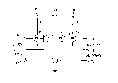
Referring to Fig. 2, the description will proceed
to an analog multiplier according to a first embodiment
of this invention. Similar parts are designated by like
reference numerals.
- The analog multiplier comprises a first pair of
transistors Ql and Q2, a second pair of transistors Q3
and Q4, and the current source Io~ The transistor Ql has
a base electrode connected to an input terminal Tl and a
collector electrode connected to an output terminal T5.
The transistor Q2 has a base electrode connected to an
input terminal T2 and a collector electrode connected to
an output terminal T6.
21 lG~32
The translstor Q3 has a base electrode connected to
an lnput termlnal T3 and a collector electrode connected to
the output termlnal T6. The translstor Q4 has a base electrode
connected to an lnput termlnal T4 and a collector electrode
connected to the output termlnal T5. The current source Io ls
connected to emltter electrodes of the translstors Ql' Q2' Q3'
and Q4. The analog multlpller has two reference termlnals T8
and T9 each of whlch has a reference voltage of zero level.
A voltage of (1/2)Vl ls applled between the lnput
termlnal Tl and the reference termlnal T8. Namely, the lnput
terminal Tl ls supplled wlth the voltage of (1/2)Vl. A voltage
of (-l/2)Vl ls applled between the lnput termlnal T2 and the
reference terminal T8. Namely, the lnput termlnal T2 ls
supplled wlth the voltage of (-l/2)Vl. A voltage of {(1/2)Vl -
V2} ls applled between the lnput termlnal T3 and the reference
termlnal T9. Namely, the lnput termlnal T3 ls supplled wlth
the voltage of {(l/2)Vl - V2}. A voltage of {(-1/2)Vl - V2} ls
applled between the lnput termlnal T4 and the reference
terminal T9. Namely, the lnput termlnal T4 ls supplled wlth
Z0 the voltage of {(-1/2)Vl - V2}.
When the lnput termlnals Tl, T2, T3, and T4 are
supplled wlth the voltages of (l/2)Vl, (-1/2)Vl, ~(1/2)Vl -
V2}, and {(-1/2)Vl - V2}, the output termlnals T5 and T6 are
supplled wlth output currents of IL and IR,respectlvely.
64768-304
2110332
In Fig. 2, collector currents of ICl, IC2, Ic3~
and IC4 in the transistors Ql' Q2' Q3~ and Q4 are repre-
sented by following equations (15), (16), (17), and (18).
VBE + (1/2)Vl)
ICl = Isexp~ T J ( 15)
I = I exp¦ BE ( / ) 1} (16)
Ic3 = I exp¦ BE / ) 1 V2} (17)
¦V - (1/2)V - V } (18)
In Fig. 2, inasmuch as the transistors Ql, Q2,
Q3, and Q4 are driven by the current source Io~ a
Cl' C2' C3' C4' 0 g Y
following equation (19).
Cl C2 C3 C4 F 0 (19)
A following equation (20) is given by
substituting Equations (15) to (18) for ICl, IC2, I
and Ic4 in Equation (19).
I5exp( - ) = ~FIo (20)
VT 4cosh( 1 )cosh( 2 )exp( 2 )
2VT 2VT 2VT
Consequently, a difference current of aI between
IL and IR is represented by a following equation (21).
L IR (ICl + IC4) - (IC2 + IC3)
(VBE)sinh( 1 )sinh( - )exp( ) (21)
VT 2VT 2VT T
2110932
A following equation (22) is given by
substituting Equation (20) for Isexp (VBE)/(VT) in
Equation (21).
aI = ~FIOtanh{(Vl)/(2VT)}tanh{(V2)/(2VT)} (22)
Inasmuch as ~F is approximately equal to "1", ~F
is approximately equal to ~F2. Consequently, by
comparing Equations (13) and (22), it will be understood
that the ~I is approximately equal to the ~I'.
Referring to Fig. 3, characteristic curves A, B,
C, and D represent the characteristic of relation between
input signals and output signals in the analog multiplier
of this invention. The characteristic illustrated in
Fig. 2 is substantially equal to the characteristic of
the conventional analog multiplier illustrated in Fig. 1.
Referring to Fig. 4, the description will proceed
to an analog multiplier according to a second embodiment
of this invention. Similar parts are designated by like
reference numerals.
The analog multiplier comprises the transistors
Ql to Q4, the current source Io~ and a voltage supplying
circuit VSC. The voltage supplying circuit VSC comprises
transistors Q5 to Q13, first and second resistors R, and
first through third current sources Il each of which has
a current of Il. Il is equal to (1/2)Io.
The input terminal Tl is connected to a first
input terminal Tll. The input terminal T2 is connected
to a second input terminal T12. The transistor Q5 has a
base electrode connected to a third input terminal T13.
2110932
12
The transistor Q6 has a base electrode connected to a
fourth input terminal T14.
The analog multiplier is supplied with a first
input analog signal having a voltage of Vl and a second
input analog signal having a voltage of V2. More
specifically, the first and the second input terminals
Tll and T12 are supplied with the voltage of Vl. The
third and the fourth input terminals T13 and T14 are
supplied with the voltage of V2.
A collector electrode of the transistor Q5 is
connected to collector electrodes of the transistors Q7
and Q9 and to emitter electrodes of the transistors Qll,
Q12, and Q13. Emitter electrodes of the transistors Q5
and Q6 are connected to the first current source Il.
Emitter electrodes of the transistors Q7 and Q8 are
connected to the second current source Il. Emitter
electrodes of the transistors Q9 and Q10 are connected to
the third current source Il. A collector electrode of
the transistor Q6 is connected to a collector electrode
of the-transistor Qll. A base electrode of the
transistor Q7 is connected to the input terminal Tl and
the first input terminal Tll. The transistor Q8 has a
base electrode connected to the input terminal T3 and a
collector electrode connected to a collector electrode of
the transistor Q13 and the input terminal T3.
The transistor Q9 has a base electrode connected
to the input terminal T2 and the second input terminal
T12. The transistor Q10 has a base electrode connected
21109~2
13
to the input terminal T4 and a collector electrode
connected to a collector electrode of the transistor Q12
and the input terminal T4. The transistor Q11 has a base
electrode connected to a base electrode of the transistor
5 Q13 and to the collector electrode of the transistor Q6.
The output terminal T5 is connected to a node of
the emitter electrodes of the transistors Q12 and Q13
through the first resistor R. The output terminal T6 iS
connected to a node of the emitter electrodes of the
transistors Q12 and Q13 through the second resistor R. A
first output terminal Tl 5 is connected to the output
terminal Tl. A second output terminal T16 iS connected
to the output terminal T6.
The voltage supplying circuit VSC receives the
voltages of V1 and V2 and produces the voltages of
1 / )V1, {(1/2 )V1 - V2~, and {(-l/2)Vl - V } to
supply the voltages of ( 1/2)V1, (-1/2)V1, {(1/2)V1 - V2~,
and ~(-1/2)V1 - V2} to the input terminals T1, T2, T3,
and T4, respectively. When the input terminals T1, T2,
T3, and T4 are supplied with the voltages of ( 1/2)V1,
(-1/2)Vl, {(1/2)Vl - V2}, and {(-1/2)Vl - V2~, the output
terminals T5 and T6 are supplied with the output currents
of IL and IR, respectively. Also, an output voltage of
VO occurs between the first and the second output
terminals T15 and T16. The voltages of VO is
proportional to DI, namely, (V1~V2).