Note: Descriptions are shown in the official language in which they were submitted.
~ W 0 92/22429 - 1 - 211 ~ O ~ 2 P~T/GBg2/0l08s
Multi-Channel Array Droplet Deposition Apparatus.
This inv~ntion relates to mulSi-channel array droplet deposition
apparatus and to a method of ~anufacture thereof.
In European Pa~ent No. 0,277,703 and Europçan Patent No. 0,278,590,
there i~ disc10~2d multiochannel 8rray droplet d~po~i~ion ~pparatus,
suitably, ~or use as dropoon-deDand ink ~et printheads and of the form
comprising an array of parallel channels ~utually spaced transversely to
the channels in the ~rray direction. The~e printheads e~ploy piezoelectric
actua~ors forming at lea~t par~ of the channel separating side walls as the
means for effecting drople~ ~xpul~ion from nozzl~ communicating
re~p~ctively with the channels. One preferred me~hod of m~king such a
printhe~d co~prise~ providing a ba~e sheet having a layer of piezoeleetric
material poled no~mal thereto, for~ing 8 ~ultiplicity of parallel grooves
the layer of p~ezoelectric materialL so that the Dla~cerial af~ords channel
eparatin~ w lls between ad~acent grooves, the ~nk channels thus bein~
provided by the groov~s, forDting electrodes on the channel facing surfaces
of the walls so that the actuating elec~cric fields are applied nor~sl to
~he direction of poling in the array direc:tion to produce deflection of the
wells ln the direction of the applied fields, connecting electrical drive
oircuiLt~ to the elec~rode~, bondin~ a top sh~et t~ the walls 'co close the
inlc channels, providinK nozzles for the respectlve channels and further
providing ink ~upply ~ean~ co~unicating with the channels.
In one design, the channels ~eparating walls co~prise piezoelectric,
so~called, "chevron" actuPtors in which upper and lower parts of the walls
are oppositely poled so as to deflect into chevron for3ll transversely to ~che
corre~ponding channels. One method of forming the base shcet from which
the channels and channel separating wall actuators are formed consists of
.. , .. . . . , .. . .. . . .. , . . ~ . . . .. . . . .
W O 9~/22429 PCT~GB92J~ 5
Q 8 ~
using a five layer lamin~te a~ disclosed in PCT ~pplication No.
PCT/~B91/02093. In an alternative design, there are employed, so-called,
"cantilever" actuators which are disclosed in ~uropean Patent Application
No. 89309940.8 (Publication No. 0,3S4,136). In PCT P~tent Application No.
PCT/GB91/00720 there ~s disclo~ed an ~rray of parallel ink chsnnels Por~ed
fro~ a ~umber of like modul~s each h~ving a ~ultiplicity of parallel ink
channels, the modules being ~erially butted ~ogether. In a preferred form
pair~ of the but~ed ~odule~ form an ink channel at the butting locstion.
It is a general ob~ect of the present invention to provide a
multi-channel array, droplet deposition apparatus of improved const~uction
and an imp~oved ~ethod of manufacturing sald app~rstus. Another object is
to enable ~he p~vi~ion of a mult~-~h~nel array dr~plet deposition
apparAtu~ whi~h c~n operate at lower vol~age ~or a giv~n compli~nce of the
channel wall actuators.
It is a further ob~ect of one ~OI~ of the present inv~ntion to provide
a ~ulti-channel array, droplet deposition app~ratus ~nd a ~ethod of
manu~acture thereof ~n which the integri~y of the chip co~nections to the
track~ whieh connect with ~he ~hannel elec~r~de~ is not threa~ened by
~her~l cycli~g of the printhead.
The presen~ invention con ists in a method o~ manufac~uring a
~ul~i ch~nnel array droplet deposit~on app~ra~us which co~pri~es providing
a ba~e sheet havin~ a layer of p~ezoelectric ~aterial poled normal to said
sheet9 ~orming an array of parallel, op~n-topped droplet liquid channels in
said base ~hs~t layer ~o that the piezoelectric material provides
upst~nd~ng wall5 separating successive channels, forming electrodes on
ohannel facing surfaces of the walls7 bonding a channel closure sheet to
the walls, providing nozzles re~pectiYely communicating with the channels
, .~ , ~, . . .. . . .
~ WO 92/22429 2 ~ ~ ~ O ~ 2 p~/G~92Jo108s
~d providing means for connecting a source of dropl~t liquid to ~he
chalLnels, characteri~ed by forming said channel closure sheet with ~ array
of parall~l conductive track~ spaced at intervals correspondin~ with the
channel ~pacing. locating the ch~nnels in position par~llel` with and
opposlte ~aid ~rack.~, and ~ealirlg the closure sheet ~o the ch~el walls by
forming bonds which mechanical~y ~nd electrically cor~nect each track to the
electrodes on the chau~nel facing sides of the walls of the ch~nel opposi~e
~here~co. Preferably, the ~ethod include~ connecting drive current circuit~
to the tra~k~ prior to for~ng -~aid bonds to connect e~ch o~ the tracks to
the electrode~ on ~he channel facing side~ of the walls o~ the channel
opposi~e ~hereto. Advantageously, the ~ethod includes forming said bonds
as . older bond Preferably, the method includes d~positing solder on
~ither or both th~ tr~ck~ and the elec:trodes, locating 'che channels
opposite the track~ and si~ultaneou~ly ~or~ing the bonds to coDnec~ the
tr~cks eash to the el~ctrode~ OI the ~haTmel fa~ing sur~ace~ of the walls
o~ the channel oppo~te thereto. A180 the m~thod preferably includes
h~ating at le~t the solder thereby to c~use ~che solder to wet the tracks
and the d~oining electrodes thereby to ~or~ a meniscus bridging the trac}cs
and ~d~s~ining el~ctro~ and cooling the ~older to for~ ~aid bond~.
Advan~cageou~12rO the ~ethod al80 includes f'orming s~d tracks on said
channel clo~ure ~heet o~ width approaching that o~ the spacing of the
el~ctrodes on the channel ~cing w~
The i~vention f'urther co~ists in a multi-channel array droplet
depocition appar~tus eomprising a base sheet having a layer o~
piezoel~ctric ma'cerial poled nor~ 1 thereto, an array of parallel, open
~opped, droplet liquid channel~ in said bas0 sheet layer provided by
upstanding ch~nnel separating walls formed in ssid layer, electrodes
W O 92/2~429 PCT/GB92/~ 5
2111Q~
provided on channel facing surfaces of the wslls~ a chann~l closure sheet
bonded to the walls, noz~les re~pectively co~municatlng with the channels
and means for supplying droplet liquid to th~ channels~ characterised in
that said channel closure sheet h~s an array o~ par ~ 1 conductive tracks
thereon ~paced at interv21~ correspondlng with the ~h~nnel spacing and
diæposed parallel with and opposite the channels and bonds mechanicslly ~nd
electrically connect each track to the electrodes on ~he channel facing
walls of the ~hannel opposite thereto and ~eal the closure sheet to the
channels. Suitably, electric drive curren~ circuits are connected
re3pectively to the tracks. Advantageously. the tracks on the channel
clo~ure shee~ are of width approaching ~ha~ of the spacing between the
electrode~ on the channel facing wall~O Pre~erably, the bond~ connecting
~he track~ to ~he electrodes a~e solder bond~. Adv~n~ageously, ~he solidus
of the ~older o~ the bonds i~ ~elected,.h~ving regard to the values of the
ther~al e~pansion coe~icients, to l~it th~ r~l~tive ~hermal ~r~ins of
the channel clo~ure sheet and said piezoelectr~c material. The solder can
be an alloy of lead and/or tin and/or indium. One alloy which may be
employed co~pri~es lead and ~in. In a preferred ~r~ the soldQr is a
eutectic ~lloy i~clud~ng lead ~nd tin. In a ~urther ~orm the solder alloy
i~clud~s s~lver.
Suitably, ~he channel closure sheet compris~s a glass or ceramic
having a relatively high elaxtic modulus compared with ~hst of
piezoelectric eeramic and an expansion coe~ficient matched to that of <110>
silicon. A preferred ~aterial for the channel clnsl~re sheet is
borosilicate gl~ss. This type of closure sheet may have deposited thereon
a lsyer of crystalline silicon extending the width o~ the sheet in ~he
channel array direction said layer of silicon having for~ed therein a
WO 9~/22429 PCI'/GB92/01085
211~0~
multiplexer drive circuit having input and output ~er~inals of which ~he
output terminals are connecte~ ~o ~he conductive tracks on the channel
closure sheet.
The invention will now be dec~cr~bed by . way of' ~pl~ by rePerence to
the aocolaparlyin~ diagra~s of' which:
FI~RE: 1 ~hows a longitudinal sectioII of a droplet deposition
apparatus ln the form of a drop~on demand inlc ~et prlrAthead constructed in
accordance with the invention;
FIGURE 2 ~how~ a section in the array direotion on 'che line X-X of
Figure 1 of one for~ OI the prln~chead; and
FIGURE 3 ~how~ a ~ection in the array direction on the line X-X of
Figure 1 of ~o~her for~ o~ t~se printhead.
In th~ ~rawing~ like part~ are referred to by ~he ~ane reference
erals.
Figure.Q 1 to 3 illustrate fo~s o~ ink ~et array printhead which are
~3~bled according ~co the principles of the inverltion. Ihe printheads are
of :the drop-on-demand type incorporat:lng channel div~ding wall actuators.
These sctuator~ are ~rf~ed in a ~hee:~ of piezoelectric ceramic poled in ~
directioll p~ ndicular to ~he ~h~et and operated in ~hear ~ode so thst the
a~tuator~ deflec~ in the d~rec~Gion of the electric f'ield applied thereto.
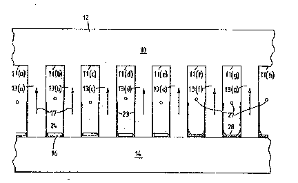
me drawings illu~trate a printbead 10 in which an array of ink
Channe!l8 ll(al....ll(h~, separa~ed by channel separating wall actuators
13~a)...13(g) forEed in a sh~et of piezoelec~ric ceramic 12~ are bonded ~o
a ~ub~trate or ehannel clo~ure ~heet 14. The substrate has parallel
eonductive tracl:^~ 16 ~orD~ed thereon at the same pitch interval as ~he ink
channels. The tracks 16 are connec~ced to drive chip 27 and conduct
W O 92/22429 P(~r~GB92/~
0 8 ~ - 6 -
electric drive signals directed from ~he chip to ~he actuators, generally
as described i~ European Patent No. 0,277,703 and European Patent
0.278~590, which introduced this class o~ drop-on-de~and printhead and the
contents of which ~re herein incorporated by referen~e~ Some aspects of
the con~ruction are Purther di~cloæed in PCT Patent Application No.
PCr/~B91/00720 ~he con~ent~ of which are also inco~porated herein by
reference. m e drive chip 27 i8 also connected to tracks 18 at one end of
the closure sheet 14 on which are provided input clock, power wave~orm ~nd
print data signsls.
The ink channels of the printhead are terminated at corresponding ends
thereo~ by nozzle 22 formed in nozzl~ plate 20 which is attached to the
piezoelectric ceramic sheet 12 and the cha~nel elosure sheet 14 remote ~rom
the chip 27. ..
A ~ni~old 21 is attached at the end of the chan~els adjacent the
drive ~h~p 27 to hold ~k and deliver it into the printhead channels via
the transverse duct 26.
The con~truction and operation of typical forms of pr$nthead in
a cordance with the invention are di~closed in ~ore detail wi~h ref~rence
to ~igur~ 2 and 3, which ~how alt~rnativ~ designs in enlarge~ents.on
~ection X-X of Fi~ure 1. Figure ? illustrates a printhead whi~h
incorporates a canSilev0r actuator as de~cribed in European Patent
Application No. 89309940.8 (Publication No. Ot364.136) the contents of
which ar~ incorporat~d herein by reference and in which the piezoelectric
c~ramic i~ polari~ed perpendicular to the plez~electric sheet in a single
orientation and in which the electrsdes 23 on the wall actuators extend
about halr the extent of the wall height: and Figure 3 illustrates a
chevron actuator made from a piezoelectric laminate as disclosed in PCT
!' `~ W 92/22429 PCI'~GB92/01085
7 ~ 2 ~
application No. PCr/GB91/02093 the content~ of which arP incorporated
herein by reference and for which ~he elec~rodes 25 extend the full height
of the wall actuators which are formed of two oppositely poled par~s in the
upper and lower halves of the walls respectively fo~ in ~wo
piezoelec~ric ceramic sheets poled in the thicknes~ direc~ion thereof. The
direction o~ poling i~ given by arrow 17 in Figure 2 and by arrows lg in
Figure 3.
An e~ ential feature of the con3truction, which is illustrated in
Figure~ 2 and 3, is that the trac~s 16 which each extend substantislly ~he
dis~ance be~ een, as the case may be, ~he electrodes 23 or 25 are coa~ed
with a ~ilm of solder 24. I~e electrodes on the actuator walls may also be
coated wi'ch a ~chin la~er of solder. ~is layer a~3ists the solder when
heat~d above its liquidus to wet the elec~crode~ e channel array is
moun~ o that ~he ink chsnnels are loca~ced parall~l with and respec~ively
opposite the soldered tracks ~nd the acltu~tor wslls occupy the ~paces which
~eparate ~che tracks. When th~ solder is heated it melt~ and flows ~or~ing
a meni cus 28 of ~older, whlch corulects electrically and ~echanically the
elec~rode~ on the walls on bo~h ~ide~ of each channel ~o the tracks on the
~ubs'crate or closure ~heet 14 at ~he sa~e ti~Ç! seallng the ink channel
wall~ to the ~ub~trate 14 in ink tight manner.
~ e solidu-~ of the ~older of the bonds is selected having regard to
the values of the thermal expansion coefficients to limit the relative
~hermal strains of the closure sheet ~nd the piezoeleetric ~naterial and can
be an alloy of lead and/or tin and/or indium. One suitable alloy comprises
lead a~d tin and is preferably a ~utectic alloy thereof. A further
suitable forn of solder alloy includes silver.
W O 92/22429 PC~rJGB92/r"~85
211~0$~2 - 8 -
The advantages o~ this const~uction are that it provid~s i~provements
both in manu~acture and performance of the printhead. These combine to
reduce the printhead cost.
In manu~ac~uxe this construction i convenient}~-simpl~Pied becau~e it
combines an e~ectronio substra~e component and a printhead component that
can be fabricated and te~ted sep~rately. When bo~h work sati~fac~orily in
test, ~hen the a~e~bly of wo~king componen~s is made by a ~older bond:
this is a rapid s~ep c~pable of au~omation and high yield in manufac~ur~.
Further the assembly can be tes~ed. Since the chip can in one design be
part of the substrate componen~, a reduction of the component count may
then be obtained.
~ n~ ~ault ~ha~ has been observed to occur on a prin~head component is
tha~ the continuity of ~he plat~ng on a small number of electrode walls is
80meti~8 interrupted by a cra~k or by local ~hading of ~h~ electrode~ and
She track during ~h~ plating process pbssibly by dust. Because, if applied
to the electrodes, the ~older, ~ince iL~ wet~ both ~he el~ctrodes associa~ed
with the track, will bridge this ~ort o~ defect, th~ pre~en~ construction
e~n to be ~el~ repairiDg with respect ~o thi~ ~ault condition. In
previous des~gns th~ ch$p~ were ~s e~bl~d to the co~pleted printhead. As a
consequence a ~aulty connectlon or a faulty chip reduced the a3se~bly
yie1d. The application o~ the channel clo~ure sheet by glue bonding also
took time ~or ~he glue bond to cure and frequently proved to be variable in
, . I
quality. The yield of the cov~r bonding process thu~ was deleterious to
the overall a~e~bly yield. ~roken pl~tin~, which is di~icult to find by
inspection, ws~ al~o a cau~e of faulty production. Printhead assembly
employing a solder connection process as described avoids these defects and
has consequently improved yield.
~ W O 92/22429 PCT~GB92~01085
~?~ 'V3`~,
Where the printhead comprises an array of like ~odules it will be
preferred tha~ the substrate channel clo~ure ~heet will generally be made
in one piece the full width of ~he array. The piezoelectric components,
however, are formed of a width appropriate to the supply of piezoelectric
~aterial (P~T) wsfers and the yield of the channel ~orming and plating
pro~esses. It will be evident that the number of ~rac~s opera$ed by each
chip on the substrate clo~ure sheet and th~ width of the piezoelectric
co~ponent~ a~embled to it can now be made independently withou~ any width
correspondence between the ~hlp~ and the active co~ponents at the butted
~oinQ, as was a feature of PCT Patent Application No. PCT/GB9l/00720. The
~ul~lple chlp~ in the array can conveniently be operated by one ~et of
input signal tracks l8 in3te~d of one 58t of tracks per chip.
A further advantageous property of the solder bond is that it holds
the w~ rigldly to the substr te channel clo~ure sheet, preventing
~ove~ent o~ the actu~tor wall~ bo~h t~r~ionally in fl ~ re and laterAlly in
~he~r. Further, i~ the track~ are formed on a rigid ~ub~trate, rotation of
the tops of the walls is sec~red preventing tip flexure. In the case of
glue bond~ 8e~l~ng the wall~ to a cha~nel clc~ure ~heet~ however, it has
been observed that the tops of the actuator walls defor~ to such a degree
that a pin ~oint is e~ectiv~ly ~ormed at the top~ of the wall~. This
ocour~ due to the relatively low ~ti~nes~ of a ~lue compared wlth that of
the solder and the actuator cera~ic.
The advantag~ of a rigid joint as opposed to a pin joint bond is
illu~trated by the f'ollowing table of performance calculations ~or a
chevron actuator such as is depicted in Figure 3.
"
WO 92/22429 ~ 0 ~ 2 I"CI/GB92/~ 85
Voltage Compllallce Wall Wall Channel
Ratio Height Wid~h Width
Volts
Pin Joint 27-5 0.353 375 ~7 80
P~igid Join~c 18 . 9 0 . 360 420 87 80
Calcul~tlons show that the wall height, to obtain a speci~ied
compliance rat~o, of' the ac~uator is greater by about 13,X when ~he bond
corre ponds to a rigid ~oint as oppo~ed to 8 pin joint. The actua~ion
voltage is also reduced by about 27%.
A lower ac'c~lating voltage Dlak~8 it possible to work ~t a lower
actuation energy ~nd also to employ a ohip made by a cheaper process. Less
heat ic alsc generated in the array during actuatior~.
ln ~rder to take be~t adv~ OI these aspects of the printhead
de~ t i-q preferred thnt ~he ~ubst.rate channel closure sheet 14 should
be ~ormed of a ~a~eri~ which ha~ a ~la$ively rigid ela~ic ~odulus and
pos~e~e~ a thermal exp~nsion coeffi::ierit ~chat i~ cl~ely ~atched b~th to
he piezoelec~cric cera~mic coolpor~ent and to the ~ilicon ~hip. ~ile the
elastic Elodulu~ of PZT is a~ut 50 ~a and the solder ~odulus is a:Lso
comparable, that of the ~ubstra~e i~ preferably greater. me ~ ion
. .
coef~icient of PZT 'cerlds to bs var:Lable depending on the supply ~ource and
proce~s hi~tory, but is preferably ~atched to that of the substrate to
about 1 part per 10 6perC~ ~e~e thermal expansion objec~ives are met
b~ the u~e o~ a boro~ilicat~ gla~s substrate such as Pyrex (Corning 7740)
or equivalent mate~al~. Since the elastic modulus of this gla~s exceeds
ZOO GPa, 'che substrate i5 e~fectively rigid.
When the substrate channel closure sheet is a borosilicate glass,
who~e expansion coæfficient matches that of silicon in the <110> direction~
.~ WO 92/22429 P~lGB92/0108$
the chip c~n be integrated on the ~ubstrate~ First a layer o~ crys~alline
silicon is deposi~ed over ~he width of the glass substr~e .in the region of
the chip 27. The logic and power ~cransi~tors of the ~ultiplexer drive
circuits are then formed directly on the silicon l~,er. Th~ ~racks 16 and
18 are then deposited so ~hat connections are made respectively with ~che
input and s~utpu~ t~r~inals of th~ drive circuit. This drive circuit is a
Dlultiplexer circui~c ~ubstantially as de~cribed in Europeas~ Paten~
Application No. 8g304573.2 (Publicasion No. 0,341,929~. In ~his way the
drive circuit i3 formed directly on ~e gla~3s substrat~ instead of ~he
chips being made on a silicon wa~er, diced into separate chips and bonded
co~ponents into the Sracl~ on the substrate.
The depo~ition of chip~ on gla~ has been prac~ ed :Eur oth~r
~ppl~cations ~uch a~ di~pl~ product~ ~nd i. advan~cageou~ provided the
~nu~aeturing yi~3ld for the chip on gl~3 proCeg~ i8 u~icien~ly ~at, ~o
that ~anu~acture a3ad as~bly of ~eparate corDponent~ by discre~ce chip
a~se~bly proce3se~ 18 Im,~UQtlfied.
A ~urther advantage in the ~anufac:ture of the piezoelectric ceramic
sheet de cribed is that mach~ tolerances a~ ~ound to be relaxed when
~he tracks are for~ed orl a separ~te substr~te char~nel elosure sheet. The
cha~el depth t~lerEmoe is gre~ter ~han that whioh is pv~sible in the prior
art proce~es referred to where ~hallow cornection g~ves are formed ln
ali~en'c wlth 'ch~ channels and separated therefrom by respeotiYe bridge
sections. Because the channels of the c~tructioQ which is describ~d
her~in are c~f usli~or~n depth throughout, control of the thickness tolerance
of the PZr la~rer can be relax~d. As result only the top face of the
piezoelectric sheet needs to b~ ground to a flatness suitable for bonding.
The control of parallelness between opposite f~ces of the PZT layer can
:,
WO92/22429 PCr/GB92/~ S
- 12 -
0 8 ~ - .
also be rel~xed. The cost of grinding one ~ace is le~s ~han that of
lapping both faces parallel. Anot~er advantage during assembly is that
connecting the substrate and the piezcelectric ~heet with e low temperature
~older i~ a rap~d step involving melting and ~olld ~ i~nl~ the sold~r, instead
of, as in the prior art7 curing ~he bond m~erial, which r~quire a
subs~antially longer cycle tim~ at the same time the solder as it wets,
holds the ~racks and the electrodes of each part automatically in alignment
and draws the~ together with a pre~sure e~ual to a few atmospheres,
avoiding the need for a~embly ~igs. The de~i~n enables automated
a~se~bly.
The construc~ion ~lso introduce~ feature~ that provide improved yield
in ~nufacture and ~mprov~d reliability during operation. One
considerasion i~ that both ~he ~ub~trate par~ and the pi~zoelectric
actuator par~ are able to be prete~ted to e~tabli~h that ~ ey are correotly
workin~ sub-co~ponent~ prior to a~e~bly.
Further the adoptlon o~ solder as a bond or eonnection material i~
advantageous, firstly becau~e i~ doe~ not hydroly~ or dissolve in the inks
~ 11108t glue bonds are found to do~ o it o~n be reheatsd and repaired,
i~ the ~older conrlect~on is not properly made.
It will be apprecia'ced tha~ with the ~tructure deseribed, the unit
co~prising the pr~nthead channels ~nd their closure ~heet can be ~eplaced
without repl~ce~ent of the chip 27 being requlred. As the chip form~ a
i
sign~Pic~nt ele~ent in ~he C05t oP the structure ~nd as it is l~ss
vulnerable to wear and damsge than the printhead channels, it is desirable
that it should not have to be changed together with the printhead
channels .
, ,, ,, . ,, .. ~ ~, , -,.. ,., . .. , , .. -.-