Language selection

Search

Patent 2112252 Summary

Third-party information liability

Some of the information on this Web page has been provided by external sources. The Government of Canada is not responsible for the accuracy, reliability or currency of the information supplied by external sources. Users wishing to rely upon this information should consult directly with the source of the information. Content provided by external sources is not subject to official languages, privacy and accessibility requirements.

Claims and Abstract availability

Any discrepancies in the text and image of the Claims and Abstract are due to differing posting times. Text of the Claims and Abstract are posted:

  • At the time the application is open to public inspection;
  • At the time of issue of the patent (grant).
(12) Patent Application: (11) CA 2112252
(54) English Title: ARBITRARY WAVEFORM GENERATOR ARCHITECTURE
(54) French Title: ARCHITECTURE DE GENERATEUR DE FORMES D'ONDE QUELCONQUES
Status: Deemed Abandoned and Beyond the Period of Reinstatement - Pending Response to Notice of Disregarded Communication
Bibliographic Data
(51) International Patent Classification (IPC):
  • H03K 04/00 (2006.01)
  • G06F 01/03 (2006.01)
(72) Inventors :
  • DURBRIDGE, LYNDON JOHN (Australia)
(73) Owners :
  • COMMONWEALTH OF AUSTRALIA (THE)
(71) Applicants :
  • COMMONWEALTH OF AUSTRALIA (THE) (Australia)
(74) Agent: SMART & BIGGAR LP
(74) Associate agent:
(45) Issued:
(86) PCT Filing Date: 1992-06-23
(87) Open to Public Inspection: 1993-01-07
Examination requested: 1999-02-15
Availability of licence: N/A
Dedicated to the Public: N/A
(25) Language of filing: English

Patent Cooperation Treaty (PCT): Yes
(86) PCT Filing Number: PCT/AU1992/000305
(87) International Publication Number: AU1992000305
(85) National Entry: 1993-12-22

(30) Application Priority Data:
Application No. Country/Territory Date
PK6861 (Australia) 1991-06-25

Abstracts

English Abstract

2112252 9300737 PCTABS00019
A method of direct digital synthesis of linear frequency
modulated wave forms comprising the steps of: at a given regular time,
adding a fixed frequency increment word (1) to a frequency control
value stored in a first register (4) to produce a lineally
increasing frequency control word; adding the frequency control word
stored in the first register (4) to a second register (8) to form a
quadratically increasing phase word; converting the
quadratically increasing phase word to an amplitude value using a lookup
table stored in a memory means (9) to produce a lineally increasing
frequency, and periodically resetting the frequency control word
to produce a frequency sawtooth. Also a device for implementing
the method being an arbitrary waveform generator comprising a
pluraality of accumulators (4+5, 7+8), a memory means (9), a convertor
means (10) and a clock means (6).


Claims

Note: Claims are shown in the official language in which they were submitted.


WO 93/00737 PCT/AU92/00305
CLAIMS
1. An arbitrary waveform generator comprising:
a plurality of accumulators each adapted to produce an output value from one
or more input values;
one or more memory means adapted to map the output of one or more
accumulators to an amplitude value;
a converter means adapted to convert the amplitude value from digital form to
analogue form; and
a control means adapted to synchronise the operation of the plurality of
accumulators, the one or more memory means and the converter means.
2. The arbitrary waveform generator of claim 1 further comprising a
plurality of input registers adapted to store the input values.
3. The arbitrary waveform generator of claim 1 in which each
accumulator comprises an adder means adapted to add two input values to
produce an output value and a register means adapted to store said output
value.
4. The arbitrary waveform generator of claim 3 in which one of the input
values is the previous value stored in the register means.
5. The arbitrary waveform generator of claim 1 in which the memory
means is addressable solid state memory.
6. The arbitrary waveform generator of claim 1 in which the memory
means contains a look-up table for mapping the accumulator output to the
amplitude value.
7. The arbitrary waveform generator of claim 1 in which the converter
means is a digital to analogue conversion device.
8. The arbitrary waveform generator of claim 1 in which the control
means is a microprocessor means adapted to provide a clock reference signal
to which the waveform generator is synchronised.
9. The arbitrary waveform generator of claim 1 in which the control

WO 93/00737 PCT/AU92/00305
means comprises a microprocessor means, reference clock means and
synchronising signal means working in cooperation to synchronise the
operation of the waveform generator.
10. The arbitrary waveform generator of claim 1 further comprising a
filter means adapted to filter the output of the converter means.
11. An arbitrary digital waveform generator comprising:
a plurality of accumulators each adapted to produce an output value from one
or more input values;
one or more memory means adapted to map the output of one or more
accumulators to an amplitude value; and
a control means adapted to synchronise the operation of the plurality of
accumulators and the one or more memory means.
12. The arbitrary waveform generator of claim 11 in which each
accumulator comprises an adder means adapted to add two input values to
produce an output value and a register means adapted to store said output
value.
13. The arbitrary waveform generator of claim 12 in which one of the
input values is the previous value stored in the register means.
14. The arbitrary waveform generator of claim 11 in which the memory
means contains a look-up table for mapping the accumulator output to the
amplitude value.
15. An arbitrary waveform generator for generating a linear frequency
ramp comprising :
first and second accumulators each adapted to produce an output value from
two input values wherein one of the input values to the first accumulator is a
frequency increment word and the output of the first accumulator is the input tothe second accumulator;
a memory means adapted to map the output of the second accumulator to a
sinusoidally varying amplitude value; and
a control means adapted to synchronise the operation of the plurality of
accumulators, the one or more memory means and the converter means.
16. The arbitrary waveform generator of claim 15 further including a

WO 93/00737 PCT/AU92/00305
converter means adapted to convert the amplitude value from digital form to
analogue form.
17. The arbitrary waveform generator of claim 15 in which each
accumulator comprises an adder means adapted to add the two input values
to produce the output value and a register means adapted to store said output
value and further characterised in that the value stored in the register means
is one of the inputs to the adder means.
18. An arbitrary waveform generator for generating a linear frequency
modulated continuous wave waveform comprising:
a control means incorporating a reference clock;
a first accumulator adapted to produce a linear frequency progression by
incrementing a frequency register by the value of a frequency increment word
once every reference clock cycle;
a second accumulator adapted to produce a quadratic phase progression by
adding the linear frequency progression to a phase register once every clock
cycle; and
a memory means adapted to produce a linearly increasing frequency ramp
from the quadratic phase progression by mapping from a sinusoidal look-up
table.
19. The arbitrary waveform generator of claim 18 further including a
digital to analogue converter adapted to convert the linearly increasing
frequency ramp from digital form to analogue form.
20. The arbitrary waveform generator of claim 18 in which the linearly
increasing frequency ramp is defined by :
the frequency increment word;
an initial frequency value stored in the frequency register prior to a first clock
cycle;
an initial phase value stored in the phase register prior to the first clock cycle;
and
a duration of the ramp being the number of clock cycles for which increments
occur.
21. A method of direct digital synthesis of linear frequency modulated
waveforms comprising the steps of:
at a given regular time, adding a fixed frequency increment word to a

WO 93/00737 PCT/AU92/00305
11
frequency control value stored in a first register to produce a linearly
increasing frequency control word;
adding the frequency control word stored in the first register to a second
register to form a quadratically increasing phase word;
converting the quadratically increasing phase word to an amplitude value
using a look-up table stored in a memory means to produce a linearly
increasing frequency; and
periodically resetting the frequency control word to produce a frequency
sawtooth.
22. The method of claim 21 further including the step of converting the
amplitude value from digital form to analogue form in a converter means.
23. The method of claim 21 further including the step of filtering the
output of the converter means.
24. The method of claim 21 in which the look-up table is a sinusoidal
look-up table.
25. The method of claim 21 wherein the given regular time is provided
by a reference clock means.
26. An arbitrary waveform generator as herein described with reference
to the attached figure.

Description

Note: Descriptions are shown in the official language in which they were submitted.


' WO 93/00737 . PCI`/AU92/00305
21~ 2252
.
ARBITRARY WAVEFORM GENERATOR ARCHITECTURE
~'
;~' BACKGROUND OF THE INVENTION
This invention relates to a method of digitally generating linear frequency
modulated continuous wave (FMCW) waveforms at high frequency for use in
5 such applications as high-freq~ency radar systems.
In its most general sense the invention can be applied to any system requiring
virtually any waveform. In this discussion its application in HF radar systems
will be used as an example.
.~
;j Signal sources used in HF radar systems require very high dynamic range,
10 low phase noise and amplitude accuracy over a wide frequency band. In
many applications they also require fast frequency switching and known
~, phase characteristics. Typical signal sources use one of two methods to
generate these signals - phase~ locked loop synthesis or direct digital
~; synthesis.
15 Phase locked loop methods, in their most simple form, suffer from poor phase
noise andlor poor~ frequency resolution~ a relative large step between
permissible frequenciss). Frequency sw~itchîng time can also be rather poor
(long).~ Direct ~digital~synthesis methods are usually based on phase
accumulator techniques or memory look-up techniques. These techniques
20 allow for both low phase~noise and~narrow 1requency resolution. However,
. , ~ ~ ~
the phase accu~mulator design is optimised for the generation of a fixed
frequenc~ tone~an~d~the memory; lookup technique suffers from large
~3 ~ computational overheads as~all data points must be calculated in advance.
This invention combines and ~extends thé phase accumulator technique to
25 provide a device~which can gerlerate arbitrary or pseudo-arbitrary waveforms.This is particularly important~in a real-time~system. The invention described
here~ may~be used as a pseudo-arbitrary wavetorm generator with high
capability and low com~putational overhead. ~
A common waveform used in HF radar systems is the linear frequency
30 modulated continuous wave ;~FMCW) waveform, where the frequency is swept
linearly up or down~ over a programmable frequency span in a programmable
; ~
: : ~: ~

WO 93/00737 Pcr/Avg2/0030~
2 '~ 5 2 2 ~
sources it is necessary to approximate the desired waveform by a series o~
short fixed-frequency steps. This invention can produce true linear FMCW
waveforms. The technique may be further extended to produce more complex
5 waveforms of higher order, or these waveforms may be approximated by a
piecewise linear approximation. This approximation, being a second order
approximation, is inherently more accurate than the first order approximation
of conventional phase accumulator techniques.
The continuous time equation for a single cycle of a sawtooth waveform
10 (linear FMCW ramp) is given by:
f(~) = 511~1[t {~I)o I 2T t}]
where T = the period of the waveform
= 2~fo the starting;frequency of the ramp
~1 = 2~1fj the ending frequency of the ramp.
15 Converting this equation to an ~equivalent discrete time equation with
sampling period ts ~and adding the constraint that there are an integer number
~N) of samples in a ramp period, reveals that it can be written more simply as:
~ :
f(n) = SlN[n(a + bn)l
:
where ~ a =
20 ~ ~ ~ ` b -~ 2~N ~
This~analysis leads to the~discovery that a discrete digital synthesis ramp
generator: may be implemented with~two levels of accumulation and a
;; sinusoidal look-up ROM if the~two phase registers are loaded with the initial values a + b and 2b~ r*spectiv~ly. ~ ~ ~
25 The technique of cascading accumulators can be extended to allow the
- generation of hlgherorder~waveforms. In fact anywaveform s(t) = SlN(~t))
where
~(t) = ao+a1t + a2tZ + ...~+antn
:

P~/AU / 9 2 / O 0 3 0 5
R CEI\/E~ 0 8 JAI'~ lg93
~1122~2
can be generated with n cascaded accumulators. By including a cosine
lookup ROM as well as a sine lookup ROM any waveform s(t) = eJ~(t) can be
generated. Note also that the lookup ROM is not constrained to sinusoidal
waveforms, but can be used to map any periodic function. In practice
5 implementing further stages of accumulation becomes difficult due to a need
for greater arithmetic precision in the early stages of accumulation, and to
account for propagation delays through the accumulator chain. The design
presented here àpproximates higher order waveforms by a piecewise linear
approximation.
1 0 SUMMARY OF THE INVENTION
According to perhaps one form of this invention there is proposed an arbitrary
waveform generator comprising:
a plurality of accumulators each adapted to produce an output vatue from one
or more input values;
1 5 one or more memory~means adapted to map the output of one or more
accumulators to an ampl~tude value;
a converter means adapted to convert the amplitude value from digital form to
analogue form;~ and~
a control means adapted to synchronise the operation of the waveform
2 0 generator.
In prsferenGe ~the input va~lues are stored in a plurality of input registers.
In preference thè ~converter; means is a digital to analogue converter that
c onverts a digital ~signal from the digital section of the generator to an
analogue~sbnal.; ~
2 5 In preference the~ memory~means is an addressable solid state memory device
such as a rea~ only~memory device containing a look-up table for mapping a
linear variation in; phase to~ a sinusoidal variation in amplitude. Alternatively,
the merr~ory~means~couid be an EPROM, Beta card, DRAM or other similar
memory device.~The memory device look-up table may contain other periodic
3~ ~functions. ~ ~ ~
In preferencè the control~ means is a microprocessor incorporating a clock
means which is a~high purity oscillator. In order to interface to the very
cemplex waveiorm scheduling requirements of on operational OTHR radar
I ~
E~SU85TITUTE SHEEr¦
.

- W0 93/0073t ~ PCI /AU92/0030
' control system a high performance microprocessor is required.
,, :
In preference there is provided a filter means which filters the output of the
digital to analogue converter. In praetice this is a low pass filter.
In a further form of this invention there is proposed a method of direet digital5 synthesis of linear frequ~ney modulated waveforms eomprising the steps of:
at a given regular time, adding a fixed frequeney increment word to a
frequency eontrol value stored in a first register to produce a linearly
inereasing frequeney eontrol word;
adding the frequeney eontrol word stored in the first register to a seeond
10 register to form a quadratieally inereasing phase word;
eonverting the quadratieally inereasing phase word to an amplitude value
;'i ~ using a look-up~table stored in a memory means to produee a linearly
inereaslng frequeney; and ~ ~ ~
periodieally resetting the frequeney eontrol word to produee a frequency
1 5 sawtooth. ~ ~ ~
In preferenee~the~ amptitude value is eonverted from a digital value to an
analogue value~using a digital to analogue eonverter.
;~ In preferenee there is provided a~ tiiter means after the digital to analogue
converter~and~in preference this is a low pass filter.
20 In preferenee there is provided a eloek means to provide the given regular
: timeandcontrolthe~periodlc~resening~
' '~ DESCRIPTION OF THE PREFERRED EMBODIMENT
For~a b~er understanding ~of;this' invention~a~ preferred embodiment will now
be described~with rèfèrenee to;the~attaehed drawing in whieh: -
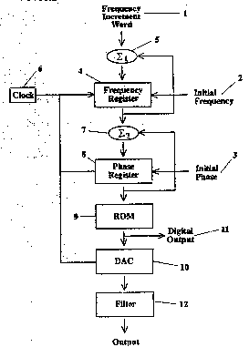
'25- ~ ~ FIG~ is a~schematic of an~ arbitrary~waveforrn generator consisting of two
phase accu mulator stages.; ~
: ~
Ph~se accumulator signal synthesis is a digital technique whereby a fixed
phase increment~is added~to a value stored in a phase register, giving rise to alinearly varying phase. ~As the instantaneous frequency is defined to be the
~ ~ ~ 30 time derivative~ of the phase, the phase~ accumulator thus generates a fixed
,~ ,,~;, - : .
, ~ ~

WO 93/00737 PCr/AU92/0030~S
5 2112252
frequenoy signat. This signal is mapped to an amplitude by a sinusoidal
lookup table, which may then be converted to an analogue form by a digital-
to-analogue converter.
Referring in detail to the figure, the inputs to the generator are a frequency
increment word 1, an initial frequency 2 and an initial phase 3. The frequency
register 4 is incremented in an adder 5 by the value of the increment word 1
on each reference clock pulse of a clock 6, giving a linear frequency
progression. The llnearly chan~ing frequency output trom the ~requency
register 4 is added in adder 7 to the phase register 8 on each clock pulse to
produce a quadratic phase progression which is mapped by the ROM 9 to
produce a linearly increasing frequency ramp. By resetting the control values
at regular intervals the output becomes a repetitive frequency sawtooth A
digital to analogue converter 10~ converts the digital signal 11 to analogue
form which is subsequently~passed through a low-pass filter 12 to produce the
desired output.
Each ramp can be completely defined by four parameters or control values:
initial phase, initial frequency, trequency increment word and duration of
ramp. Any of the first three parameters may be unused (taking the final value
of the previous r~amp),~ which allows for~reater flexibility in waveform
generation and reduces some computational overhead.
A logical extension;~ of this technique is to implement more stages of
` ~ accumulation to ~generate~ polynomials of higher order, allowing even more
complex waveforms to be~generated directly. However, current technology
imposes restrictions on the capabi!ity~of such higher-order polynomials, such
25 ~ ~ that it is presently more appropriate to generate these higher-order
polynomials in a~piècewise linear approximation using short linear FMCW
ramps. ~
~; ' The method of controlllng this dual phase accumulator allows independent
setting of the initia!~phase, initia! frequency, and frequency deviation rate It~; 30 also allows pseudo-arbitrary~waveforms to be generated relatively simply by
~means of piecewise~Onear approximation with short time intervals (possibly as
short as 10-20 microseconds). This is a very powerful method of generating
pseudo-arbitrary waveforms, as the length of the waveform sequence is
dependent only on the~ storage requirements for the waveform definition,
rather than on the storage requirements for the entire sequence (as in the
:

WO 93/00737 ` PCI'/AU92/0030~ .
L~ " ~
211Z252
memory lookup method of arbitrary waveform synthesis). It also allows real-
time generation of data points, avoiding the long overheads of memory lookup
techniques.
The waveform generator may be configured to either repetitively generate the
5 same ramp or produce a series of independent ramps. Pseudo-arbitrary
waveforms can be generated by a piecewise linear approximation of ramps to
the desired waveform instead of using a muleiple accumulator architecture of
higher order. As each ramp segment is defined by four parameters only it is
possible to reduce the minimum ramp duration to the time required to transfer
10 these four parameters to the appropriate registers. With current high
performance microprocessors a minimum step size of 10 to 20 microseconds
is a physically achievable value that will provide a good approximation to
most desired waveforms. The pseudo-arbitrary waveform is implemented as a
series of short frequency ramps approximating the desired waveform. The
15 total number of ramp segments tha~ can be put in a sequence has yet to be
determined, but will number in the thousands and will be limited only by
~ ~ parameter storage~ requiremen~s. The speed of programming and
j ~ implementing these ramps as well as the maximum number of ramps is
determined only by the speed and~storage capabilities of the controlling
20 microprocessor.; ~This is a very~powerful method of producing pseudo-arbitrary
waveforms and allows very~complex waveforms of long duration to be
generated relative~ly simply~without recourse to multiple accumulator
architectures.~
The `invention~offers~a number of advantages. The output frequency can be
25 ~ ~ ~changed~ very~ rapidly w~thout~impacting on the quality ot the output signal.
The~ non-pipe!ined~ nature of the ~design~allows the output frequency to change
within ~a single~sampling cbck period.~ Furthermorc, any changes in frequency
are~contr~lled to~provide non-discontinuous changes in phase and frequency
$.~ ~ unless discontinuity is desired~, in whi¢h case the discontinuity is known and
30 can thus be contro~ lled; ~
In~the same manner as a singie phase accumulator is optimised for a fixed
frequency tone, the ~dual accumulator is optimised for quadratic phase
generation (i.e. Iinear FMCW). The addition of further stages of phase
$~ accumulation provide;a mèthod for optimised generation of higher order
~, 35 waveforms. Being all ~digital the phase and amplitude are controlled at all
times. This has~ particular importance in radar systems where a coherent
$

W093/00737 7 21i2~5~ P~/AU92/0030~
detection process is implemented. Coherent detPction requires a known,
repeatable phase progression and phase errors translate directly to errors in
detection.
,.
,
,1 :
'1
,, ~
; :
~: ' ::
`:

Representative Drawing
A single figure which represents the drawing illustrating the invention.
Administrative Status

2024-08-01:As part of the Next Generation Patents (NGP) transition, the Canadian Patents Database (CPD) now contains a more detailed Event History, which replicates the Event Log of our new back-office solution.

Please note that "Inactive:" events refers to events no longer in use in our new back-office solution.

For a clearer understanding of the status of the application/patent presented on this page, the site Disclaimer , as well as the definitions for Patent , Event History , Maintenance Fee  and Payment History  should be consulted.

Event History

Description Date
Inactive: IPC from MCD 2006-03-11
Application Not Reinstated by Deadline 2002-06-25
Time Limit for Reversal Expired 2002-06-25
Inactive: Abandoned - No reply to s.30(2) Rules requisition 2001-12-27
Inactive: S.30(2) Rules - Examiner requisition 2001-06-26
Deemed Abandoned - Failure to Respond to Maintenance Fee Notice 2001-06-26
Inactive: Status info is complete as of Log entry date 1999-03-05
Inactive: Application prosecuted on TS as of Log entry date 1999-03-05
Inactive: RFE acknowledged - Prior art enquiry 1999-03-05
All Requirements for Examination Determined Compliant 1999-02-15
Request for Examination Requirements Determined Compliant 1999-02-15
Application Published (Open to Public Inspection) 1993-01-07

Abandonment History

Abandonment Date Reason Reinstatement Date
2001-06-26

Maintenance Fee

The last payment was received on 2000-04-27

Note : If the full payment has not been received on or before the date indicated, a further fee may be required which may be one of the following

  • the reinstatement fee;
  • the late payment fee; or
  • additional fee to reverse deemed expiry.

Patent fees are adjusted on the 1st of January every year. The amounts above are the current amounts if received by December 31 of the current year.
Please refer to the CIPO Patent Fees web page to see all current fee amounts.

Fee History

Fee Type Anniversary Year Due Date Paid Date
MF (application, 5th anniv.) - standard 05 1997-06-23 1997-06-02
MF (application, 6th anniv.) - standard 06 1998-06-23 1998-04-20
Request for examination - standard 1999-02-15
MF (application, 7th anniv.) - standard 07 1999-06-23 1999-04-19
MF (application, 8th anniv.) - standard 08 2000-06-23 2000-04-27
Owners on Record

Note: Records showing the ownership history in alphabetical order.

Current Owners on Record
COMMONWEALTH OF AUSTRALIA (THE)
Past Owners on Record
LYNDON JOHN DURBRIDGE
Past Owners that do not appear in the "Owners on Record" listing will appear in other documentation within the application.
Documents

To view selected files, please enter reCAPTCHA code :


To view images, click a link in the Document Description column (Temporarily unavailable). To download the documents, select one or more checkboxes in the first column and then click the "Download Selected in PDF format (Zip Archive)" or the "Download Selected as Single PDF" button.

List of published and non-published patent-specific documents on the CPD .

If you have any difficulty accessing content, you can call the Client Service Centre at 1-866-997-1936 or send them an e-mail at CIPO Client Service Centre.

({010=All Documents, 020=As Filed, 030=As Open to Public Inspection, 040=At Issuance, 050=Examination, 060=Incoming Correspondence, 070=Miscellaneous, 080=Outgoing Correspondence, 090=Payment})


Document
Description 
Date
(yyyy-mm-dd) 
Number of pages   Size of Image (KB) 
Description 1995-07-28 7 539
Abstract 1995-07-28 1 89
Claims 1995-07-28 4 255
Description 1999-03-21 7 311
Drawings 1995-07-28 1 43
Representative drawing 1998-12-16 1 11
Reminder - Request for Examination 1999-02-23 1 117
Acknowledgement of Request for Examination 1999-03-04 1 173
Courtesy - Abandonment Letter (Maintenance Fee) 2001-07-23 1 182
Courtesy - Abandonment Letter (R30(2)) 2002-03-06 1 172
Fees 1998-04-19 1 32
PCT 1993-12-21 9 309
Fees 1997-06-01 1 33
Fees 1999-04-18 1 29
Fees 2000-04-26 1 30
Fees 1995-06-04 1 46
Fees 1994-05-15 1 41
Fees 1996-05-07 1 33