Note: Descriptions are shown in the official language in which they were submitted.
/
- FlLE, Plt~l~ THIS AP~lENDCD
F TRANSLATION
1 - 2~2~
D E S C R I P T I O N
EXTERNAL MODULATOR FOR OPTICAL COMMUNICaTION
TECHNICAL FIELD
This invention rela~es to an external modulator
for optical communication for applying a modulation
signal to an optical fiber from the exterior and
thereby indirectly modifying a light propagating in
the optical fiber, and more particularly to an
external modulator for optical communication which can
be easily manufactured, which can suppress the
resonance of elastic waves in the optical fiber, which
has a small insertion loss so that a large number of
external modulators can be connected to a single
transmission line, which has a flat frequency
characteristic, and which can be used for high
frequency modulation.
BACKGROUND ART
Conventionally, most of the modulators
incorporated in an optical communication system
generally utilize a direct modulation system for
cha~ging an application current to a semiconductor
laser or light emitting diode which is a light source
and directly modulating an output light therefrom.
However, in the case of this system, there is a
problem that the light property is made unstable
according to the modulation of the intensity in an LD
(laser diode) generally used as a light source and the
transmission distance of an optical signal is
considerably limited.
' ; ;`~'
:
-
2~2~
-- 2 --
Further, in this system, one signal source
(signal transmission source) is used as to correspond
to one transmission line, it becomes necessary to
insert an optical coupler between the individual
signal source and the transmission line in order to
couple optical signals composed of a plurality of
signal sources into one transmission line.
However, in the above direct modulation system,
an insertion loss caused by the insertion of the
optical coupler is large. For example, even in a case
of a waveguide type optical coupler whose insertion
loss is said to be relatively small, it is approx. 0.5
dB. Therefore, the number of signals which can be
coupled to one transmission line is limited.
In order to overcome the above limitation in the
direct modulation system, recently, a modulator
utilizing an external modulation system is developed.
The external modulation system is a system having
a D.C. light source whose intensity is constant with
time, and modulating a propagation light by use of a
modulator arranged on a half-way of the optical
transmission line and can exclude obstacles based on
instability of the light source. Further, it has an
advantage that the insertion loss caused when the
modulator is inserted to the optical transmission line
is small, and therefore, a large number of modulators
can be incorporated into the optical transmission
line.
As a modulator incorporated into an optical
communicatlon system of the above external modulation
system, the following examples are known as
representative examples.
.
~ ~.
~..
- 3 ~ 21~2'~
One of them is obtained by forming a waveguide
pattern having a large refractive index in a substrate
made of LiNbO3 by ion exchanging operation, for
example, and disposing an electrode for voltage
application near the waveguide.
The external modulator is opera~ed on the basis
of the electrooptic effect, and the modulation
characteristic in the high frequency region (several
GHz) is excellent, but the dependency thereof on
variations in the temperature and moisture is large,
the dependency of the light output intensity on the
bias voltage fluctuates according to deterioration
with time and expansion/contraction of the waveguide
base plate caused by the above variations, thus
providing a problem that it is difficult to attain the
stable operation. Further, since the single crystal
of LiNbO3 is extremely expensive and has a difficulty
in the practical application in the industry. In the
case of this modulator, the insertion loss is as large
as 2 to 4 dB, and therefore, it is difficult to
dispose a large number of modulators in one optical
transmission line.
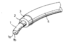
Further, there is provided such a type as shown
in FIG. 1 and disclosed by D. S. Czaplak and F. S.
Hickernell in Ultrasonics Symposium, 1987, pp 491 to
493. The external modulator has such a structure that
the outer periphery of a clad layer la of a single
mode optical fiber 1 is covered with a lower electrode
which is formed of a Cr-Au thin film, a thin film 3
formed of ZnO which is a piezoelectric material and an
upper electrode 4 which is formed of a Cr-Au thin
film.
~ .
_ 4 _ 2 1 ~ 2 '1~ ~ -
Further, Godil et al. proposed a structure
constructed by laminating a lower electrode 2 formed
of Cu/Au and a piezoelectric thin film 3 formed of
ZnO, sequentially and partially on a half~portion of
the periphery of the optical fiber as shown in FIG. 2
in J. Lightwave Technol vol. 6, 1586, 1988. In the
case of the above external modulator, an unnecessary
resonance mode of elastic waves can be suppressed not
by orientating the stress of the elastic waves
concentrated on a core lb of the optical fiber
symmetrically with respect to an axis of the optical
fiber, but by orientating the same perpendicular to
the axis.
In the above external modulators, since the
optical fiber and the external modulating means are
formed in an integral structure, there is provided an
advantage that the insertion loss in the transmission
line is extremely small and they can be manufactured
at a low cost.
However, in the case of the above external
modulators, the lower electrode, piezoelectric thin
film, and upper electrode are formed by applying the
vapor deposition method or sputtering method, but
since the surface of the optical fiber l is a curved
surface, it becomes necessary to rotate the optical
fiber in the film forming device or use other high-
degree operation technology in order to form a
piezoelectric film having a uniform piezoelectric
characteristic over the entire range of the
circumferential direction, thus providing a problem in
the manufacturing process.
Further, there is provided a problem of the
2~2~
-- 5
characteristic that the elastic wave is considerably
reflected on the periphery of the optical fiber so as
to cause the resonance of the elastic wave inside the
optical fiber, and as a result, the frequency
characteristic of the modulator cannot be made flat.
Further, D. B. Patterson et al. made public a
type as shown in FIG. 3 in Optics Letters, vol. 14,
No. 4, 1989, pp. 248 to 250.
The external modulator has a structure obtained
by sequentially laminating a lower electrode 2, a thin
film 3 of ZnO and an upper electrode 4 in this order
on one-side surface of a substrate 5 made of quartz
glass, forming a groove 5a of a semi-circular cross
section on another surface, and closely burying a
single mode optical fiber 1 in the groove 5a.
Like the modulator proposed by Hickernell et al.,
the above external modulator has an advantage that
since the insertion loss thereof in the transmission
line becomes extremely small and the surface of the
substrate 5 is flat, the film thickness control for
the lower electrode 2, piezoelectric thin film 3 and
upper electrode 4 can be made easy respectively, ~
therefor a uniform characteristic can be obtained over ~--
the entire surface.
However, in the case of the above external
modulator, it is extremely difficult to work the
groove 5a formed in one surface of the substrate 5 of
quartz glass so as to exactly coincide with the
curvature of the cross section of the single mode
optical fiber 1 which is closely buried in the groove.
Further, for the same reason as in the case of
Hickernell and Godil, the resonance phenomenon occurs
2~2~
-- 6 --
in the optical fiber and the frequency characteristic
of the modulator is not made flat.
Further, since the velocities of elastic waves
(sound waves) propagating in the substrate 5 and the
optical fiber 1 are substantially the same, the
elastic wave propagates straightforwardly at the
portion of the interface between the substrate 5 and
the optical fiber 1, thus making it difficult to
effectively converge the elastic wave into the core of
the optical fiber 1. Particularly, when the driving
frequency is high, the directivity of the elastic wave
generated in the piezoelectric thin film 3 is
extremely sharp and the elastic wave propagates
straightforwardly in the substrate 5 so that the
amount of the elastic wave which is converge into the
core of the optical fiber 1 will be extremely limited.
That is, the rate at which the elastic wave generated
in the piezoelectric thin film 3 contributes to
modulation of the light propagating in the optical
fiber 1 is extremely small and the efficiency is
lowered.
In order to improve above problems, it is
effective to increase the length/width ratio of a
portion functioning as the piezoelectric element so as
to increase the effective length of the piezoelectric
thin film for the optical fiber, but when such a -~
process is effected, the width of the piezoelectric
thin film 3 or upper electrode 4 becomes narrow so
that setting of the positional relation between the
piezoelectric thin film and the optical fiber will
require high precision, thereby making the setting
difficult.
:
- :
21~2~
-- 7
Further, the external modulators proposed by
Hickernell, Godil, Patterson have commonly the
following problems described hereinafter.
First, the amplitude of the elastic wave
generated in the piezoelectric thin film largely
depends on the film thickness. The amplitude can be
measured based on the frequency applied to the
piezoelectric thin film and the S/N ratio, and the
value thereof is set to the maximum value at the
resonance frequency fr and considerably attenuates as
the frequency is deviated from the resonance frequency
fr as shown in FIG. 4 so that the bandwidth of the
modulation frequency is narrowed accordingly.
Further, in the case of the above external
modulators, since the piezoelectric thin film is used
as a modulation medium, the piezoelectric element
section constructed by the piezoelectric thin film,
lower electrode and`upper electrode electrically
functions as a capacitor. For this reason, the
impedance thereof varies with the frequency of a ~ -
modulation signal from a modulation signal output
section which is an information source. In order to
effectively transmit the modulation signal to the ;
piezoelectric element section, it is necessary to
attain electrical matching between the modulation
signal output section which is an information source
and the piezoelectric element section.
The impedance variation of the piezoelectric
element section based on the frequency depends on the
electrical capacitance of the piezoelectric element -~
section and the electrical capacitance largely depends
on the area of the upper electrode. Therefore, the
'
: .
'
-
2 1 ~
-- 8
frequency band used to the above external modulators
depends on the area of the upper electrode. For this
reason, in the case of the external modulator having
only one upper electrode, there occurs a.problem that
only one fre~uency band which is applicable can be set
and the amount of information to be transmitted is
reduced.
In order to solve this problem, it is considered
to serially connect a plurality of external modulators
to one station. In this case, when a plurality of
external modulators are connected to one another by
use of optical fibers, they can be easily connected by
use of adapters for connectors if optical connectors
are connected to both ends of the optical fiber, but
in this connection system, there occurs a new problem :
that the insertion loss is not negligible when the
numher of connecting portions becomes large and a
light is reflected between the connectors. .
Further, if the ends of the optical fibers are
connected by fusion method, the above-described
problem concerning the insertion loss and reflection :
of light can be solved, but a problem that the
handling thereof is difficult occurs. ~ ~:
Further, as a problem common to the above two :
connection systems, a problem that the occupied space
of the modulation system is large occurs.
Further, there is provided a type made public by e
Fu~isaki et al. ln Institute of Electronics and :~
Communication Engineers at National Convention,
Spring, ~-891, 1990. The external modulator has a
structure constructed by mechanically pushing PZT ~ :
piezoelectric ceramics on a coating of single mode ~
21~2~
g
optical fiber.
However, in this type of external modulator,
since the piezoelectric element and the clad of the
single mode optical fiber are not closely contacted
together, the transmission efficiency of the elastic
wave from the piezoelectric element to the optical
fiber is degraded, and as a result, it is difficult to
say that the modulation for high frequencies higher
than 1 MHz can be adequately attained.
An object of this invention is to provide an
external modulator for optical communication in which
the insertion loss is small and which indicates a flat
frequency characteristic having no special resonance
peak and can attain the modulation for the high
frequency such as approx. 500 MHz.
Another object of this invention is to provide an -
external modulator for optical communication which can
be easily manufactured since the film thicknesses of
the lower electrode, piezoelectric thin film and upper
electrode can be easily controlled, respectively, and
in which the control of orientation of the
piezoelectric thin film can be easily attained and a
preferable piezoelectric effect can be realized.
Still another object of this invention is to
provide an external modulator for optical
communlcation in which elastic waves generated in the
piezoelectric thin film can be efficiently converged
into the core of an optical fiber so as to attain an
excellent modulation efficiency.
Another object of this invention is to provide an
external modulator for optical communication in which
the frequency characteristic of the output efficiency
21~ 2~8i~
- 10 -
of elastic waves generated in the piezoelectric thin
film is broad and the modulation frequency bandwidth
is widened.
Still another object of this invention is to
provide an external modulator for optical
communication which can transmit a large amount of
information with a single external modulator and the
occupied space of a modulation system can be made
small.
DISCLOSURE OF INVENTION
In this invention, as a first aspect, there is
provided an external modulator for optical
communication comprising:
a substrate having substantially the same acoustic
impedance as a clad layer of a single mode optical
fiber to be disposed;
a piezoelectric element section constructed by
laminating a lower electrode, piezoelectric thin film --
and upper electrode in this order on one surface of
the substrate;
at least one single mode optical fiber arranged on the
other surface of the substrate; and -~
a material coating the single mode optical fiber on at
least part thereof in a place in which the single mode
optical fiber is disposed and having an acoustic
impedance which is approximately equal to that of the
clad layer of the single mode optical fiber. -
As another aspect, there is provided an external
modulator for optical communication comprising:
a substrate having substantially the same acoustic
impedance as a clad layer of a single mode optical
- 11 21 12 ~
fiber to be disposed;
a piezoelectric element section constructed by
laminating a lower electrode, piezoelectric thin film
and upper electrode in this order on one surface of
the substrate;
at least one single mode optical fiber arranged on the
upper electrode; and
a material coating the single mode optical fiber on at
least part thereof in a place in which the single mode ::-:
optical fiber is disposed and having an acoustic ~ :
impedance which is approximately equal to that of the
clad layer of the single mode optical fiber. : ::
As still another aspect, there is provided an :
external modulator for optical communication ~ :~
comprising~
a substrate having an optical transmission line
therein and formed of a material which has
substantially the same acoustic impedance as the ~:
optical transmission line; and
a piezoelectric element section constructed by
laminating a lower electrode, piezoelectric thin film - .
and upper electrode in this order on one surface of
the substrate. ~
The above-described external modulator of the ;: ::
first aspect has a basic structure as shown in FIGs. 5 :~
to 7 and the structure is constructed to have a :~
piezoelectric element section disposed on one surface ~:
of the substrate and a single mode optical fiber ~.
disposed on the other surface thereof. ~. ::
First, as shown in FIG. 5, a thin film-form lower .
electrode 2, a piezoelectric thin film 3 and a thin :
film-form upper electrode 4 are laminated in this
' ' ' . -; '~ , , ~ :
- 12 _ 211 2~
order on one surface 6a of a flat plate-form substrate
6 formed of quartz glass and having a thickness of 1
mm, a length of 20 mm and a width of 20 mm, for
example, so as to form a piezoelectric element section
A and leads 7a, 7b for introducing an electrical
signal for driving the piezoelectric thin film 3 are
respectively attached to the lower electrode 2 and the
upper electrode 4. r ..
The material of the substrate 6 is not limited to
the above-described quartz glass, but any material
having substantially the same acoustic impedance as
the clad layer of the single mode optical fiber -~
disposed on the substrate can be used, and an Si
substrate or sapphire substrate can be used, for -
example.
The material of the lower electrode 2 and upper
electrode 4 is not particularly limited, but Al, Cr,
Au, Cu, Au/Cr, Au/Ta, Au/Ti may be used, for example,
and as the material of the piezoelectric thin film 3,
LiNbO3, ZnO, AlN, PVDF (polyvinylidene fluoride) can
be used, for example.
The lower electrode 2, piezoelectric thin film 3 ~-
and upper electrode 4 can be formed by the known film
forming method such as the sputtering method, vacuum
deposltion method or CVD method, for example.
At the time of film formation, since the
substrate 6 is made in the plate-like form, film
formation of the lower electrode 2, piezoelectric thin
film 3 and upper electrode 4 on the substrate can be
effected with the substrate 6 kept fixed and the
control for the film thickness can be easily attained.
Therefore, it is possible to form the lower
.
2~12~
- 13 -
electrode 2, piezoelectric thin film 3 and upper
electrode 4 whose thicknesses can be made constant
over the entire surface so that the piezoelectric
element section A can attain the highly reliable
function. Further, the orientation of the
piezoelectric thin film 3 can be easily controlled,
and the piezoelectric efficiency can be enhanced by
arranging the c axis of ZnO vs the position
perpendicularly to the surface o, the substrate 6 when -
forming the piezoelectric thin film by use of ZnO, for ~;
example.
As shown in FIG. 6 and FIG. 7 which is a cross -
sectional view taken along the line VII-VII of FIG. 5,
a single mode optical fiber 8 is disposed on the other
surface 6b of the substrate 6 in the position directly
below the piezoelectric thin film 3. More
specifically, a desired length portion of the optical
fiber 8 and the other surface 6b of the substrate are
covered with a material 9 having an acoustic impedance
which is close to the acoustic impedance of the clad
layer 8a to fix the optical fiber 8 on the substrate
6. The acoustic impedance used here indicates the
product of the density of a medium in which the
elastic wave propagates and the speed of the elastic
wave propagating in the medium.
In this case, all the part of the periphery of
the optical fiber 8 except a portion which is in
contact with the substrate 6 is coated with the
material 9.
As the above material, any material having
substantially the same acoustic impedance as the
substrate, that is, any material having an acoustic
:
.. -: : . : : , . : : . ,: ~:.. ,: , : .
2~2~
- 14 -
impedance substantially equal to the acoustic
impedance of the clad layer 8a of the single mode
optical fiber 8 disposed can be used.
Generally, the reflection coefficient of the
elastic wave (sound wave) in the interface between a
medium having the acoustic impedance of Zl and a
medium having the acoustic impedance of Z2 can be
expressed by the following expression.
( Z2-Zl )/ ( Z2~Zl )
Therefore, if the periphery of the single mode
optical fiber is coated with the above material as
described above, the acoustic impedances thereof in
the interface becomes substantially equal to each
other and the reflection coefficient in the interface
becomes extremely small. Therefore, the propagating
elastic wave can be made efficiently incident into the -
single mode optical fiber. Further, a returning
component caused by reflection of the elastic wave
transmitted in the single mode optical fiber at the
optical fiber interface can be suppressed, thereby
making it possible to suppress the resonance in the
optical flber.
As a material for attaining the above effect, for
example, ceramics obtained by dispersing fine
particles of quartz glass into sodium silicate
(NaO 4SiO 2-aq) and sintering and vitrifying the
product (acoustic impedance : 13.1x10⁶ kg/(m2 s)), by
dispersing alumina particles into sodium silicate and
sintering and vitrifying the product (acoustic
impedance : 15.2x10⁶ kg/(m2 s)), or by dispersing
zirconia particles into sodium silicate and sintering
and vitrifying the product (acoustic impedance :
2~12~jJ
- 15 -
30.1x10⁶ kg/(m2 s)), or a material obtained by
dispersing a preset amount of metal particles into a
high molecular compound to set the inherent acoustic
impedance close to that of the clad layer 8a can be
used.
In the above external modulator, a light signal
is transmitted from the D.C. light source to the
single mode optical fiber 8 and a voltage of preset
frequency is applied between the leads 7a and 7b. A
periodic pressure is applied to the optical fiber 8
from the piezoelectria thin film 3 and the refraction
index distribution is caused in the optical fiber 8 by
the external force so as to modulate the transmission
light. ~ ~
At this time, since the periphery of the optical ~ -
fiber 8 is covered with a material having an acoustic
impedance substantially equal to that of the clad
layer 8a thereof, no reflection of the sound wave
propagating from the piezoelectric thin film 3 occurs
on the periphery of the optical fiber 8 and it leaks
into the above material, thereby preventing the
resonance phenomenon from occurring in the internal
portion of the optical fiber. Thus, a flat frequency
characteristic can be attained.
FIGs. 8 to 11 show an external modulator in which
the elastic wave generated in the piezoelectric
element section A can be efficiently converged into
the core of the single mode optical fiber so that the
modulation efficiency can be enhanced in the external
modulator with the structure shown in FIGs. 5 to 7.
The above external modulator is similar to the
structure of the external modulator shown in FIGs. 5
~::
- 16 - 2112~
to 7 except that the substrate 6 is constructed with
the structure which will be described later.
That is, the substrate 6 is formed by joining two
media 6c, 6d in which the propagating speeds of the
elastic wave are different as shown in FIG. 8. In the
junction plane 10 between the two media, the junction
plane lOa between the two media lying in the position
directly below the piezoelectric element section A
makes a curved surface.
For example, if the medium 6c is formed of quartz
glass and the medium 6d is formed of flint glass, the
propagation speed of the elastic wave becomes higher
in the former case than in the latter case, and in
this case, the curved surface lOa becomes a curved
surface which is convex towards the medium 6c side as
shown in FIG. 8.
The above substrate 6 can be manufactured by
filling flint glass particles into a preset mold and
pressing them into a form of the curved surface lOa,
then depositing quartz glass particles on the above
structure, and melting the same while raising the
temperature under a high pressure.
The curved surface lOa may take a form of part of
the spherical surface as shown in FIG. 9 or part of a -
cylindrical curved surface which extends in the
longitudinal direction of the single mode optical
fiber 8 disposed as shown in FIG. 10. In other words,
the curved surface lOa is formed according to the
shape of the piezoelectric element section A.
The external modulator is operated as follows.
First, in a case where the elastic wave generated
in the piezoelectric element section A is a high
- 17 - 21~2~
frequency wave of approx. 200 MHz, for example, the
generated elastic wave can be regarded as a plane
wave. The elastic wave traveling straightforwardly in
the substrate 6 from the piezoelectric element section
A is reflected or refracted on the junction plane lOa
and the incident angle or refraction angle are
determined by the propagation speed in the respective
media 6c, 6d. As shown in FIG. 8, if the propagation
speed of the elastic wave in the medium 6c is set
higher than that in the medium 6d and the shape of the
junction surface lOa between the two media is made to
have the curved surface lOa which is convex on the
medium 6c side, the elastic wave is converged towards
the single mode optical fiber 8 as indioated by arrows
and converged into the core 8b thereof.
Therefore, if a light is made incident on the
single mode optical fiber from the D.C. light source
and a voltage of a preset frequency is applied
between the lower electrode-2 and the upper electrode
4, the elastic wave generated from the piezoelectric
element section A is converged and concentrated
towards the core 8b while propagating in the substrate
6 so that a light transmitted in the single mode
optical fiber 8 can be efficiently modulated.
In the case of the above external modulator, it
becomes permissible to slightly lower the precision of
conversion of the elastic wave and alleviate the
tolerance of the mounting precision of the single mode
optical fiber by adequately setting the curvature of
the junction curved surface lOa in the substrate 6.
FIG. 11 is a cross sectional view showing an
external modulator constructed by disposing a medium
2 1 ~
- 18 -
6c in which the propagation speed of the elastic wave
is high on the single mode optical fiber 8 side and
disposing a medium 6d in which the propagation speed
of the elastic wave is low on the piezoelectric
element section A side.
In this case, the junction plane lOa between the
two media lying directly below the piezoelectric
element section A is formed as a curved surface which
is convex on the medium 6c side. As a result, it
becomes possible to efficiently converge the elàstic
wave generated in the piezoelectric element section A
into the core 8b of the single mode optical fiber 8.
FIG. 12 is a cross sectional view of an external
modulator which is another example of the external
modulator of the first aspect in which the elastic
wave can be efficiently converged into the core of the
single mode optical fiber 8.
In the substrate 6 of the external modulator, a
groove 11 extending in the arrangement direction of
the single mode optioal fiber disposed directly below
the piezoelectric element section A in the surface 6b
which is opposite to the surface ~a in which the
piezoelectric element section A is formed and having a
curvature slightly larger than the curvature of the
single mode optical fiber 8 is formed.
The substrate 6 is formed of a medium which has
an acoustic impedance which is substantially the same -
as the acoustic impedance of the clad layer 8a of the
single mode optical fiber 8 disposed and in which the
propagation speed of the elastic wave is higher than
that in the single mode optical fiber 8 and, for
example, it is formed of aluminum or silicon single
- 21~2~
-- 19 --
crystal.
Further, the above-described groove 11 may be
formed by known mechanical work or chemical etching.
The single mode optical fiber 8 is arranged and
disposed in the groove ll. At this time, the inner
peripheral surface of the groove 11 and the outer
peripheral surface of the single mode optical fiber 8
are bonded together with the above-described medium
which has an acoustic impedance similar to the
acoustic impedance of the clad layer 8a disposed
therebetween, and thus they are acoustically coupled
and fixed together. In this case, "acoustically"
means that the acoustic impedances of them are
substantially equal to each other.
Arrangement and fixation of the single mode
optical fiber 8 in the groove ll may be attained by -
bonding and fixing the same on the interface with the
groove 11, and it is possible to additionally cover
the remaining periphery of the single mode optical
fiber 8 with the above-described material as indicated
in FIGs. 5 to 7. With this structure, it becomes -~
possible to securely fix the single mode optical fiber ~
8 and it is preferable. ~-
Next, the behavior of the elastic wave in the
interface between the inner peripheral surface of the ;~
groove 11 and the outer peripheral surface of the
single mode optical fiber 8 in the external modulator
is explained.
FIG. 13 shows a state in which the elastic wave ;
propagating in the substrate 6 is made incident on the
single mode optical fiber 8. When the driving - -
frequency of the elastic wave generated in the ~
:
21~ 2~
- 20 -
piezoelectric element section A is high, the generated
elastic wave travels straightforwardly in the
substrate 6, but at this time, Snell's law is valid
for refraction of the elastic wave in the interface
between the outer peripheral surface of the single
mode optical fiber and the inner peripheral surface of
the groove 11 in the same manner as in the case of
light.
In this case, assuming that the propagation speed ;
of the elastic wave propagating in the substrate 6 is
~ 1~ the incident angle thereof is ~ 1~ and the
propagation speed of the elastic wave propagating in
the. single mode optical fiber 8 is ~ 2~ and the :
outgoing angle thereof is ~ 2~ then ~ 1 x sin~ 2 =
~ 2 x sin~ 1 is obtained. Therefore, when v 1 is
larger than v 2~ the elastic wave is converged on a :~
portion having a curvature larger than the curvature:~
of the single mode optical fiber 8 as indicated by
arrows in FIG. 14 so that a light propagating in the
core 8b of the single mode optical fiber 8 can be
modulated extremely efficiently.
Further, as shown in FIG. 15, the elastic wave
can also be converged into the core 8b by making the
shape of the groove 11 of the substrate 6 larger than --
the curvature of the single mode optical fiber 8,
filling a space.provided between the groove 11 and the
single mode optical fiber 8 disposed therein with -
matching oil lla or the like, and then fixing the
single mode optical fiber 8 by use of the material 9.
An external modulator shown in FIG. 16 and FIG.
17 which is a cross sectional view taken along the
line XVII-XVII of FIG. 16 is formed by disposing a
- ::
- 21 - 2 1 12 ~ ~
plurality of (two in the drawing) upper electrodes of
the piezoelectric element section A in the case of the
external modulator of the first aspect with the basic
structure shown in FIGs. 5 to 7.
With the above structure, a large number (Which
is the same as the number of the upper electrodes) of
information items can be transmitted by use of a
single external optical modulator by inputting
modulation signals including different contents
cutputted from a modulation signal output section
which is an information source to each of the upper -
electrodes 4a, 4b.
Further, since the frequency band in each
modulation signal can be changed by adequately
changing the areas of the upper electrodes 4a, 4b, a
large number of information items can be transmitted
by use of a æingle external modulator. Therefore, the
occupied area of the modulation system can be made
smaller in comparison with a case where a plurality of
external modulators are used.
An external modulator shown in FIG. 18 and FIG.
19 which is a cross sectional view taken along the
line XVX-XVX of FIG. 18 is formed by commonly -
disposing a lower electrode 2 in the piezoelectric
element section A, forming a plurality of (two in the
drawing) piezoelectric thin films 3a, 3b on the lower
electrode 2, and respectively forming upper electrodes
4a, 4b on the piezoelectric thin films.
Also, with this structure, the same effect as
that obtained in the external modulator shown in FIGs.
16, 17 can be attained.
An external modulator shown in FIG. 20 and FIG.
: . - : , :: .
: ; . ... -. :, . ~ . :.. .~ :
- :
- 22 - 2 1~ 2 ~ ~
21 which is a cross sectional view taken along the
line XXI-XXI of FIG. 20 is formed by changing the film
thickness of the piezoelectric thin film 3 in the
piezoelectric element section A at a preset rate along
the arrangement direction of the single mode optical
fiber 8 in the case of the basic structure shown in
FIGs. 5 to 7. That is, it is an external modulator in ~ :
which a relatively inclined surface is formed between
the film surface of the piezoelectric thin film 3 and
the longitudinal direction of the single mode optical ~ :
fiber 8.
In the case of this external modulator, it is : :;Y:
possible to suppress the attenuation of the amplitude
of the elastic wave to a small value in the frequency
region of the elastic wave corresponding to the film
thickness of the piezoelectric thin film 3, and as a
result, the effect that the modulation frequency band ;~
width can be widened can be obtained. ~ :~
In this case, the degree of a variation in the
film thickness of the piezoelectric film thickness - :
varies depending on the frequency of the wavelength of ~- -
the light to be modulated, but it is preferable that :; :
the inclination of the single mode optical fiber 8 in - .
the longitudinal direction is roughly adjusted in a
range of 4.0 to 5.0x10⁻⁴.
Next, the second aspect in the external modulator
of this invention is formed by disposing a single mode
optical fiber 8 on an upper electrode 2 and coating a
material 9 described before on the periphery thereof
and fixing the single mode optical fiber 8 as shown in
FIG. 22.
Also, in this case, like the first aspect, since
- 23 - 2~ ~2flg ~
the periphery of the single mode optical fiber 8 is
coated with a material having substantially the same
acoustic impedance as a clad layer 8a thereof,
reflection of the elastic wave on the periphery of the
optical fiber does not occur so that the resonance
phenomenon in the optical fiber can be prevented,
thereby making it possible to attain the flat
frequency characteristic.
Further, in the external modulator with the above -~
structure, a surface 6b which is one of the surfaces
of the substrate 6 on which the piezoelectric element
section A is not formed is made as a rough surface as
shown in FIG. 23, the elastic wave which is part of
the elastic wave generated in the piezoelectric
element section A and propagates in the substrate 6 is
scattered on the rough surface 6b, and as a result,
the resonance of the elastic wave in the substrate 6
can be prevented and it is preferable.
In this case, it is preferable to set the
roughness of the rough surface such that the center
llne average roughness (Ra) defined in terms of JIS B
0601 is set to be larger than the wavelength of the -
elastic wave propagating in the substrate. For
example, in a case where the substrate is formed of `
quartz glass and the frequency applied to the
piezoelectric element section A is 400 MHz, it is
preferable to set Ra of the rough surface to 15 ~m.
Such a rough surface can be obtained by polishing
by use of abrasive grains having particle diameter of
several tens ~m, for example.
Also, in the external modulator of the above
structure, as shown in FIGs. 16 to 19, a large number
- 24 - 2 ~ 2 ~ ~
of information items can be transmitted by use of a
single external modulator by forming a plurality of
upper electrodes on the piezoelectric thin film 3 or
forming a plurality of piezoelectric thin films on the
lower electrode 2, respectively forming upper
electrodes on them, and disposing a single mode
optical fiber on each of the upper electrodes.
Further, as shown in FIGs. 20, 21, it is possible to ~
widen the modulation frequency bandwidth by making the ~-
film thickness of the piezoelectric thin film inclined '
at a preset rate in the longitudinal direction of the
single mode optical fiber disposed.
Further, as shown in FIG. 24, a lower electrode
2, piezoelectric thin film 3 and upper electrode 4 of
uniform thickness are sequentially laminated on one
surface 6a of the substrate 6 to form a piezoelectric
element section A and the other surface 6b is formed
to have an incllned surface which is inclined at a
constant rate in a direction perpendicular to the
longitudinal direction of the single mode optical
fiber 8 disposed so that the elastic wave which is
part of the elastic wave generated in the
piezoelectric element section A and which propagates
in the substrate 6 will be reflected on the inclined
surface 6b as indicated by the broken lines and can be
prevented from being returned in the same direction,
and as a result, the resonance of the elastic wave in
the substrate 6 can be prevented.
In each of the above external modulators of the
flrst and second aspects, since the single mode
optical fiber is simply bonded to and fixed on the
surface of the substrate or the upper electrode, the
- 25 - 2 1 ~2l~ ~
junction may be damaged by an external force at the
time of actual use.
For this reason, in the above external
modulators, as shown in FIG. 25, an external modulator ~ -
is disposed with the single mode nptical fiber 8 side
facing up on a base plate 12 of depressing means which
is constructed by the base plate 12 and a depressing
section 13 disposed on the upper p~rtion of the base
plate 12, having a keep plate 13b b~ased by springs
13a, 13a and vertically driven by adjusting screws
13c, 13c, and the single mode optical fiber 8 is
resiliently depressed via a silicone rubber 14, for
example, by the biasing force of the springs 13a, 13a
by adjusting the screws 13c, 13c to lower the
depressing section 13. With this arrangement, the
single mode optical fiber can be stably held and it is
suitable, and in addition, the effect that the optical
fiber and the substrate are set in close contact with
each other can be enhanced.
The third aspect of the external modulator of
this invention is made by forming an optical
transmission line directly in the substrate. - -
As the above external modulator, as shown in FIG.
26 and FIG. 27 which is a cross sectional view taken
along the line XVX-XVX of FIG. 26, a structure in
which the built-in optical transmission line is formed
of an optical waveguide 6e and a piezoelectric element
section A is formed on one surface of the substrate 6
may be used.
The above external modulator is manufactured by
sequentially laminating a clad layer formed of quartz
glass and core layer on an Si substrate 6f, for
~: . , -- . . . . .
21~2~
- 26 -
example, by the normal flame deposition method, then,
removing part of the core layer by dry etching,
forming the waveguide 6e of a preset cross section in
the longitudinal direction, burying the waveguide 6e ~:
in a clad layer 6g as the substrate 6, and forming the
piezoelectric element section A on one surface of the
substrate.
With this structure, the waveguide 6e is used as
the optical transmission line and a light propagating
therein is modulated by an action of the piezoelectric
element section A disposed directly above the same.
Further, as shown in FIG. 28, the single mode
optical fiber 8 is integrally formed as an optical
transmission line in the substrate 6 by filling a :
preset amount of quartz glass particles into a mold,
disposing the single mode optical fiber 8 thereonr
filling quartz glass particles thereon again, and
vitrifying it by sintering while applying a pressure
to the whole portion when forming the substrate 6 by :~:
use of quartz glass. Then, the external modulator of
the third aspect can be obtained by forming the
piezoelectric element section A on one surface of the
substrate 6.
Also, with the external modulator of the above
structure, transfer of a large number of information
items can be attained by use of a single external
modulator by forming a plurality of upper electrodes
on the piezoelectric thin film 3 as shown in FIGs. 16
to 19, or forming a plurality of piezoelectric thin
films on the lower electrode 2 and forming the upper
electrodes on them, and disposing the optical
transmission line in the substrate in a position
- 27 - 2~2~
corresponding to them. Further, it becomes possible
to attain an increase in the modulation frequency
bandwidth by setting the film thickness of the
piezoelectric thin film to be inclined at a constant
rate in the longitudinal direction of the built-in
optical transmission line as shown in FIGs. 20, 21.
BRIEF DESCRIPTION OF DRAWINGS
Fig. 1 is a perspective view showing a
conventional case of an external modulator; FIG. 2 is
a perspective view showing another conventional case
of an external modulator; FIG. 3 is a perspective view
showing another conventional case of an external
modulator; FIG. 4 is a graph showing the frequency ~ -~
characteristic of the conventional external modulator;
FIG. 5 is a perspective view showing the state of one
surface of an external modulator of this invention;
FIG. 6 is a perspective view showing the state of the
other surface of the external modulator of this
invention; FIG. 7 is a cross sectional view taken
along the line VII-VII of FIG. 5; FIG. 8 is a cross
sectional view showing another example of the external
modulator of this invention; FIG. 9 is a perspective
view showing an example of a medium junction surface
of the external modulator of FIG. 8; FIG. 10 is a
perspective view showing another example of a medium
junction surface of the external modulator of FIG. 8;
FIG. 11 is a cross sectional view showing another
example of the external modulator of this invention;
FIG. 12 is a cross sectional view showing still
another example of the external modulator of this
invention; FIG. 13 is an explanatory view showing the
2 1 ~
- 28 -
state in which the elastic wave propagating in the
substrate of the external modulator of FIG. 12 is
incident on the single mode optical fiber; FIG. 14 is
an explanatory view showing the behavior of the
elastic wave in a case wherein the propagating speed
of the elastic wave in the substrate of the external
modulator of FIG. 12 is higher than the propagating
speed of the elastic wave in the single mode optical
fiber; FIG. 15 is an explanatory view showing a case
wherein the elastic wave causes another behavior
different from that of FIG. 14; FIG. 16 is a plan view
showing another example of the external modulator of
this invention; FIG. 17 is a cross sectional view
taken along the line XVII-XVII of FIG. 16; FIG. 18 is ~.
a plan view showing another example of the external
modulator of this invention; FIG. 19 is a cross
sectional view taken along the line XIX-XIX of FIG.
18; FIG. 20 is a side view showing another example of
the external modulator of this invention; FIG. 21 is a
cross sectional view taken along the line XXI-XXI of
FIG. 20; FIG. 22 is a perspective view showing another
aspect of the external modulator of this invention;
FIG. 23 is a cross sectional view showing another
example of the external modulator of FIG. 22; FIG. 24
is a side view showing another example of the external
modulator of FIG. 22; FIG. 25 is a cross sectional
view showing pressing means of the external modulator
of this invention; FIG. 26 is a side view showing an
example of still another aspect of the external
modulator of this invention; FIG. 27 is a cross
sectional view taken along the line XXVII-XXVII of
FIG. 26; FIG. 28 is a perspective view showing another
2112~
- 29 -
example.of a still another aspect of the external
modulator of this invention; FIG. 29 is a block
diagram showing a measurement system for modulated
output of the external modulator; FIG. 30 is a cross
sectional view showing the fixing state of the single
mode optical fiber into a groove in the case of an
embodiment 4 of this invention; and FIG. 31 is a graph
showing the frequency characteristic of an external
modulator of an embodiment 6. .
- EM8ODIMENTS
Embodiment 1
A lower electrode 2 was formed by sputtering Al
on one surface 6a of a quartz glass plate 6 with a
thickness of 1 mm, a piezoelectric thin film 3 with a
thickness of 5 ~m was formed by sputtering ZnO
thereon, and an upper electrode was formed by
sputtering Al thereon. Then, a clad layer 8a of a
single mode optical fiber 8 with a core diameter of 8
~m was disposed on the other surface 6b of the quartz
glass plate 6. Next, a bonding agent having quartz
glass particles with grain diameter of 5 ~m dispersed
in sodium silicate was coated over a length of 10 mm
of an arrangement portion, dried and left under the
room temperature, and sintered for 2 hours at a
temperature of 150 ~. An optical fiber 8 was
integrally formed with the qualtz glass plate 6 by use
of a coating 9 of sintered body of the quartz glass
particles so as to form an external modulator with a
structure shown in FIGs. 5 to 7.
In the above external modulator, both of the
acoustic impedances of the qualtz glass plate 6 and
2~2~
- 30 -
the single mode optical fiber 8 are 13.1x10⁶
kg/(m2 s) and the acoustic impedance of the coating 9
also has substantially the same value.
100 external modulators were serially connected
by connecting the end portions of the optical fibers
of the external modulators by thermal fusion, one end
thereof was connected to a light source, and the other
end was connected to a receiving section.
An LD for emitting a light with wavelength of
1.33 nm was used as the light source and the LD was
caused to emit a light at a constant intensity so as
to make the light incident on the single mode optical
fiber. Further, the receiving section was constructed
to have a polarization element connected to the single
mode optical fiber and measure a change in the
intensity of light received at a PD (Photodiode) after
passing through the polarization element.
In this optical communication system, the loss of
light by one external modulator is caused only by the
connection loss caused by fusing the single mode
optical fibers to each other and was approx. 0.03 dB.
Therefore, the total loss of the 100 external
modulators was approx. 3.0 dB.
When a sine wave of 400 MHz to 500 MHz was
transmitted to each of the external modulators at an
lnterval of 1 MHz and all the signals obtained at this
time were measured at the receiving section, all of
the signals could be simultaneously detected.
Embodiment 2
In the external modulator shown in FIG. 8, a
piezoelectric element section A was formed in the same
manner as in the case of the embodiment 1 except that
~ . " , ., 1 ,~
- 31 - 21~2~
quartz glass was used as the medium 6d, flint glass
was used as the medium 6c, the total thickness of the
substrate was set to 2 mm, the radius of curvature of
the curved surface lOa was set to 1.25 mm, and the ~ -
height thereof was set to 0.5 mm, and the single mode
optical fiber was disposed in the same manner as in
the case of the embodiment 1.
The above external modulator was set in the
measurement system shown in FIG. 29 and an modulated
output thereof for a light having a wavelength of 1.33
nm was measured. A modulation output improved by 12
dB or more in comparison with a case wherein the
entire portion of the substrate 6 was formed of quartz
glass was measured.
Embodiment 3
An external modulator with the structure shown in
FIG. 12 was formed by forming the substrate 6 by use
of Al, forming the piezoelectric element section A
having the lower electrode 2 and upper electrode 4
formed wi~h a thickness of 0.2 ~m by use of Cr and
Au, respectively, and the piezoelectric thin film 3
formed with a thickness of 7 ~m by use of ZnO on one
surface of the substrate, forming a groove 11 having a
semi-circular cross section and a diameter of 126 mm
on the other surface thereof, setting the single mode
optical fiber 8 with a diameter of 125 mm into the
groove, bonding them together by use of the same
bonding agent used in the embodiment 1, and then
bonding and fixing them by sintering.
The external modulator was set in the measurement
system shown in FIG. 29 and a high-frequency voltage
of approx. 200 MHz was applied between the lower
'
,~
2~ ~2~s~3
- 32 -
electrode 2 and the upper electrode 4 to measure a
modulation output for a light having a wavelength of
1.33 nm.
It was confirmed that a modulation output was
improved by 10 dB or more in comparison with an
external modulator constructed by using a quartz glass
plate having the same propagation speed of the elastic
wave as the optical fiber as a substrate and forming a
similar groove.
Embodiment 4
A silicon single crystal substrate was prepared
as the substrate 6, an etching mask was formed on one
surface thereof by use of SiO2, and then an etching
process was effected by use of potassium hydroxide
solution to form a groove 11 with a cross section as
shown in FIG. 30. Next, an external modulator with a
structure shown in FIG. 30 was formed by filling
matching oil lla into the groove 11~ disposing a
single mode optical fiber 8 therein, and pressing the
optical fiber towards the substrate 6 side as
indicated by arrows so as to fix the same in the
groove. When an modulation output was measured under
the same condition as that of the embodiment 3 by use
of this external modulator, it was confirmed that the
elastic wave generated in the piezoelectric element
section A was efficiently converged into the core 8b
of the single mode optical fiber 8.
Embodiment 5
A quartz glass plate with the length of 20 mm,
width of 20 mm and thickness of 1 mm was prepared as a
substrate.
External modulators with a structure shown in
2 ~
- 33 -
FIGs. 16, 17 were formed by forming a lower electrode
with a thickness of approx. 0.2 ~m by vapor-
depositing Al on one surface of the quartz glass
plate, forming a piezoelectric thin film of ZnO with a
thickness of approx. 10 ~m on the above structure by
the sputtering method, and then vapor-depositing A1
thereon to form two strip-form upper electrodes with a
width of 0.4 J~m, length of 1 mm and thickness of 0.2
-~m so as to form a piezoelectric element section A.
A signal with a central frequency of 320 MHz and
bandwidth of 1 MHz is applied to one of the external
modulators and a signal with a central frequency of
340 MHz and bandwidth of 4 MHz is applied to the other
external modulator so as to drive the piezoelectric
thin film 3.
When a signal intensity-modulated by supplying it
through an analyzer in the measurement system of FIG.
29 was observed by passing the O/E converter and by
use of a spectrum analyzer, it was confirmed that the
two signals ware correctly transmitted. -
Embodiment 6
An external modulator with a structure shown in
FIGs. 20, 21 was manufactured as described below.
First, a quartz glass plate with the length of 20
mm, width of 20 mm and thickness of 1 mm was prepared
as the substrate 6, the lower electrode 2 with a
thickness of approx. 0.2 ~m was formed by vapor -`
depositing Al on one surface thereof, and a
piezoelectric thin film was formed on the structure by
sputtering ZnO in a strip form with a width of approx.
10 ~m and a length of approx. 10 mm. Further, the
upper surface of the piezoelectric thin film 3 is made
~ 34 ~ 2~ 3
as an inclined surface having an inclination of
approx. 2x10⁻³ in the longitudinal direction.
Next, the upper electrode 4 was formed in a strip
form with a width of 1 mm and a length 10 mm by vapor
depositing Al on the piezoelectric thin film 3.
After this, like the embodiment 1, the single
mode optical fiber 3 was disposed in position directly
below the upper electrode 4 on the other surface of
the substrate.
The external modulator was set in the measurement
system shown in FIG. 29 and evaluation for the
frequency characteristic was made by use of a light
with a wavelength of 1.33 nm.
The result is shown in FIG. 31.
As is clearly seen from FIG. 31, in this external
modulator, attenuation of the elastic wave in the
frequency region corresponding to the film thickness
of the piezoelectric thin film 3 is small, and an
increase in the modulation frequency bandwidth is
realized.
Embodiment 7
An external modulator with the structure shown in
FIG. 22 was formed.
That is, like the embodiment 1, the piezoelectric
element section A was formed on one surface of the
substrate of the quartz glass plate and the single
mode optical fiber 8 was disposed and fixed on the
upper electrode 4 of the piezoelectric element section
A by use of the bonding agent used in the embodiment
1. ,
The external modulators were serially connected
in the same manner as in the embodiment l and the same
_ 35 _ 2~ J
experiment was made. As a result, the total loss of
100 external modulators was approx. 4.8 d8 and all of
the modulation signals of 400 to 500 MHz could be
simultaneously detected.
Embodiment 8
An external modulator with the structure shown in
FIG. 23 was formed by polishing one surface of the
substrate of the embodiment 7 on which the
piezoelectric element section A was nQt formed by use
of abrasive grains with a grain diameter of 40 ~m to
make a rough surface with the surface roughness of 6.8
~m in terms of Ra.
When the same experiment as in the embodiment 7
was made, resonance of the elastic wave in the
substrate was prevented and the frequency band was
improved by 6 MHz in comparison with a case of the
external modulator of the embodiment 7.
Embodiment 9
. An external modulator with the structure shown in
FIG. 24 was formed by forming one surface of the
substrate of the embodiment 7 on which the
piezoelectric element section A was not formed into a :~
surface which is inclined with the inclination of 10 ~::
with respect to a direction perpendicular to the
longitudinal direction of the single mode optical ~
fiber 8. . -
When the same experiment as in the embodiment 7
was made, resonance of the elastic wave in the
substrate was prevented and the frequency band was
improved by 3 MHz in comparison with a case of the
external modulator of the embodiment 7.
Embodiment 10
:: 2 1 ~
- 36 -
An external modulator with the structure shown in
FIGs. 26, 27 was formed as follows.
A slab-form clad layer and a slab-form core layer
were formed by sequentially depositing quartz glass
fine particles which would make a clad layer and a
core layer on an Si substrate 6f with a diameter of
76.2 mm (3 inches) and a thickness of 1 mm by the
flame deposition method and then sintering and
vitrifying the same at 1100 ~.
Next, the core layer was subjected to the dry
etching to form a waveguide 6e of a cross section with
a width of 8 Jlm and a height of 8 ~m along the
longitudinal direction, and then, quartz glass fine
particles which would make a clad layer were deposited
and vitrified on the waveguide so as to form a
substrate which has the waveguide 6e buried in the
clad layer 6g and whose thickness is 50 ~m except the
Si substrate 6f.
Then, like the embodiment 1, the lower electrode
2, piezoelectric thin film 3 and upper electrode 4 are
sequentially laminated on the clad layer 6g to form
the piezoelectric element section A.
Next, optical fibers whose end faces were
polished were abut against both ends of the waveguide
6e to form an optical transmission line. When the
measurement for the external modulator was made in the ~ --
same manner as in the embodiment 1, the frequency band -
was improved by 7 MHz or more in comparison with a
case of the external modulator of the embodiment 7.
Embodiment 11
An external modulator with the structure shown in
FIG. 28 was formed as follows.
-
- 37 ~
Quartz glass particles with a grain diameter of 3
to 5 ~m were filled to approximately the half depth
of a mold with a depth of 1.3 mm, length of 20 mm and
width of 20 mm, then single mode quartz glass optical
fiber with an outer diameter of 125 ~m was disposed
thereon, and quartz glass particles were filled again
into the mold.
- A pressure of 1000 kg/cm was applied towards the
thickness direction under the normal temperature and a
base plate which is 1.2 mm in thickness and 20 mm in
length and width and has the optical fiber disposed
near the center of the thickness direction was
obtained. It was sintered at a temperature of 1300 C
under the normal pressure so as to integrally form the
single mode optical fiber 8 in the substrate with a
length and width of 20 mm and thickness of 1.0 mm.
Li~e the embodiment 1, the lower electrode 2,
piezoelectric thin film 3 and upper electrode 4 were
sequentially laminated on the substrate 6 so as to
form the piezoelectric element section A.
The same experiment as that of the embodiment 10
for the above external modulator and substantially the -
same result was obtained.
Industrial Applicability
An external modulator of this invention has a
small insertion loss and a flat frequency
characteristic, can be used for high-frequency
modulation, can transmit a large number of information
items, may permit the resonance of the elastic wave in
the optical fiber to be suppressed, may permit the
elastic wave to be efficiently converged into the
optical fiber, and can be easily manufactured so that
.
r ~ r.
~ . ~
- 38 - 21~2~
it can be effectively used as an external modulator
for optical communication.