Note: Descriptions are shown in the official language in which they were submitted.
2 1 12 7 3 3 CFO 9688 ~
ELECTRON BEAM-GENERATING APPARATUS, IMAGE-FORMING
APPARATUS, AND DRIVING METHODS THEREOF
BACKGROUND OF THE INV~NTION
Field of the Invention
The present invention relates to a method for
driving an electron beam-generating apparatus for -
formation of a pattern of emitted electron beams in -~-
correspon~nGe with information signals. The present
invention also relates to a method of driving an image-
forming apparatus for formation of an image with a
pattern of emltted elec~Lun beams. The present
lnvention further relates to an electron beam-
generatlng apparatus and an image-LGL ~ ng apparatus
which are driven by the above drivlng methods.
~7Ql Ated RAcknrol~n~ Art
In recent years, research and development are
being made actively and extensively regarding image-
forming apparatuses which employ an electron source
having a plurality of electron-emltting devices wired
in a matrix state: espec~Ally, thin flat display
apparatuses which employ the above devices. Fig. 3 ;
illustrates schematically an example of one device unlt
of such an lmage-forming apparatus.
The lmage-formlng apparatus lllustrated ln Fig.
3 comprlses a plurallty of electron-emlttlng devlces
"A" aLLan~ed in a plane state on a substrate 31, and
:: . .~ . . . . .
", ~
. ' : ... , ,: ' '
2112 ~33
- 2 -
the electron-emitting devices A are con~ected to wiring
electrodes 32a, 32b correspond~ng to respective
scAnn~ng lines. Above the sub~a~e 31, - ~lAtion
ele~L~odes 33 are a,~ged so as to form an XY matrlx
with the scann1ng lines, and .~u1Ate the electron beam
em~ on of eaah device in accordance with information
signals. The ~ ation elec~ode 33 has op~n1ngs 34
for pasffAge of the electron beams.
The image-fo~ ~ ng apparatus shown in Fig. 3 is
usually driven as fo11 ls. A voltage for electron
emi 88~ 0~ iS Arpl ~ ed to each of the electron-emitting
devices A on one ~cAnn1 ng llne. Modulation voltages
(ON/OFF voltages or gradation voltages for ele~,on
beams) are Arp11ed to modulation ele~odes 33 ln
a~cG.~ance wlth lnformatlon S~gnA1g for one ggAnn~ng
llne of an image. Thereby a pattern of emltted ;~
ele~u.,s pA~s1ng ~l~ouyl. the op~n1ngs 34 is formed for
the one line. The pa~e~.. of the emitted ele~Gns is
irradiated onto an image-fc ~ng - -er 35 to form one
line of the image W.e,eon. Thls process is
svccess1vely conducted for each of the scAn~ ng lines
for the image to form an entire picture image. If the ~-
image-f~ ~ng member 35 is made of a lum~ne~cent
material, the image is ~1~p1A~yed by a plurality of
luminous spots 36.
CGnven~ional methods for driving such an ~ ~~e-
fGl ~ng appa~a~s as mentioned above which has an
~ ;:
,:: :: : . ~, ,,", .. .... . . . .
,, . , . .. ~; :
:,. . .. . .. .
,, ,, , , ,:", . :
. - , , ~ , .
: . . , ~ ~ ..
2.Li?,733
-- 3 --
electron source constituted of electron-emitting
regions arranged in high density involve disadvantages
such that the ~ Ation voltages of ad~acent elec~on
beams affect each other to deflect electron beam
tra~ectories and to chAng~ size and shape of the spots
rO, ed on the 1 ~è fol 1ng - -r face, thereby
lowering the f~nen~ss of the fG, -:l image.
Fig. 4 shows a di!~advan~age of a conventional
driving method. In Fig. 4, three elec~Lon beams are
emitted respectively from electron-emitting regions
40a, 40b, 40c for one sCAnn1ng line, and the eleo~lon ~-,
beams are ~ lAted by ~ ~lAtion ele~,odes 41a, 41b,
41c. In the case where a posltlve voltage (ON voltage)
i9 applied to the modulation elec~,odes, elec~,on beams
lS are irradiated from the ele~,on-emitting regions 40a,
40b, 40c onto the corre~pQn~ing lum1n~scent members
(image-forming members) 42a, 42b, 42c. If the
electron-emitting regions are close to each other (high ~ ;
density al,angement), the ,es~ec~ive electron beams 44
are deflected and spread after pA~s1ng through the
electron beam pA~sAge open~ng 43, by the forces "f"
c~Aused by ad~acent modulation electrodes, and the spots
spread lln~es1rably on each of the lu 1ne~cent members.
In Fig. 5, three ele~on beams are emitted
from the electron-emitting regions 50a, 50b, 50c for
one ~CAnn1ng line, and the electron beams are modulated
by the modulation ele~L~odes 51a, 51b, 51c. In the
. ~:
- : . . ,, ~ .-.
r) 3 3
-- 4 --
case where a positive voltage (ON voltage) is applied
to the modulation elec~.odes 51b and 51c and a negative
voltage (cut-off voltage) to the modulation electrode
51a respectively, the electron beams 54 from the
S ele~-on-emitting regions 50b, 50c pass through the
ele~.~n p~ss~ge openin~s 53, and thereafter the
tra~ectories of the ~pe~ive ele~.on beams 54 are
deflected by the fo.aes "f" e~ ed by the adJacent
~ -lation ele~L.~de~ 51b, 51c, as shown in Fig. 5, and
the spots fc ~d on the 1~ lneScent m~ ~e_s 52b, 52c
are asy -~-ic
As shown in the above le7 ~19~ in the
con~en~lonal driving method for an lmage-fo- ~ng ~:
apparatus employlng an ele~Lon source in whlch a
plurallty of el~,on-emlttlng reglon~ are a~aryed,
each ele~ron beam em1sslon pa~e." for the gC~nn1ng
line varies in elee~on beam traJectories, spot sizes,
and spot ~hAr9~ which makes difficult the formation of
fine, sharp, high-con~ast 1 -j~y This problem is
serlous, in partla~ r, in color image-fo~ ~ng ..
a~p~.atus in which red, blue, and green lumln~scent
members are sequentially arranged as image-fo lng
~ , heG~ the afo.~- ~r~ioned variation ln
ele~.on beam traJectories, spot sizes, and spot ~h~re9
c~llse~ col~ on of the elec~on beams ~g~ln~t
li lnescen~ members of unin~ended colors to give a less
rep.od~-lhle image of lower color purity and color tone
~ .,. . .. : . : . . . . ..
, ,,,, , . .. :. . .. ... . . .
,, - . . , , -:
-: , -- ~
" :: ~ ' ' i ' ' ' ': '': ' '
,
: .,
: ,.. ,. ~
, ; , ~ ": ,.
, : , . . , . : ". : ,:.. : : i .;.. .. . ... .
2:~ I 7733
irregularity, which makes it ~ ~5~1 ble to high density
aL~any~ s~t of the l~ ~nescent - '~rs. The above
disadvan~age is much more serious when the voltage (ON
voltage) of the ~r~ul~tion elee~-ode ls raised in order
to inorease the quantity of ele~ons rA~oh~ ng the
~ -je fol ing ~ '-r. Therefore, it is ~ acLicable
to increase sufficiently the quantity of the electron
irradiation onto the image-forming member and to raise
the luml n~nce and the contrast of the image as desired. ~ ~ ~
~' ~ '''
SUMMARY OF T~ INVRNTION ~ -
An ob~ect of the p,esenL invention is to
provlde a drivlng method for an 1 -j forming apparatus
and an electron beam-ganera~ing apparatus to obtaln an
lmage with hlgh f~nA~ess, hlgh sharpness, and hlgh
contrast.
AnGW.eL ob~ect of the present lnventlon is to
provlde a drlving -W-od for an lmage-foL ~ng apparatus
and an ele~son beam-generatlng apparatus to obtain a
full-color image wlth ehL.F -ly less lrregularlty of
color tone wlth high color ~ep~o~ c~hlllty.
Accordlng to an aspect of the present
lnventlon, there is provided a drlvlng method for an
electron beam-gene,atlng apparatus havlng an electron
source havlng a plurallty of electron-emltting devlces,
and a plurallty of modulatlon me~ns for modulatlng
electron beams emltted from the electron source in
: . . .: I ,! . ~ ~ ,', ~, -; .: .
_ - 6 - ~ ~127~3
correspon~ence with information slgnAls, the driving
method comprising applying a cut-off voltage to a first
~ Atlon means ad~acent to a seco--A -7vlAtion means
to which an ON voltage is Appl~e~ as the lnformation
signals in ~dlll ation of the electron beam.
According to a further aspect of the present
$nvention, there is provided an ele~on beam~
generating apparatus having an ele~on source having a
plurality of ele~son-emlttlng devices, and a plurality
of modulation means for modulatlng electron beams -~
emitted from the eleu~,Gn sou,ce in corre~pQ~e~ce with ~ ;
lnformatlon sigrAls, which i8 driven by the method
~a~ed in the p,ece~ng ~a,~,aph.
According to ano~her aspect of the present
invention there is provided a driving -~I,od for an
elec~,on beam-g~ne,a~ing apparatus having an ele~,on
sou,~e having a plurality of ele~,on-emitting devices,
and a plurality of modulation means for modulating
ele~,un beams emitted from the eleuL,ûn soulce ln ~ i
c~,,e~o~d~nce with infol ~ion s~gnAls~ the driving
method comprising dividing lnformation Q~gnAlQ into a ~
plurality of portions and inputting each of the A ~,
portions to the ~ atlon means succesQ~vely in
modulation of the ele~lon beams.
Accordlng to a further aspect of the present
invention, there ls provlded an electron beam-
g6ne,ating apparatus having an ele~,on source having a
:L2733
- 7 -
plurality of electron-emitting devices, and a plurality
of modulation means for modulating electron beams
emitted from the electron source in col~&p~dence with
information s~gn~ls~ which is driven by the method
stated in the preced~ n~ paragraph.
According to still another aspeat of the ~
present invention, there is provided a driving method -
for an ele~,on beam-generating apparatus having an
ele~,on source having a plurality of elee~lon-emitting
devices, and a plurality of modulation means for
modulating elec~,on beams emitted from the ele~-on -~
~o~,~e in co,~6~po~ence with information 9~gn~ls, the
drlvlng method oomprlsing dividing information s1gnAl~
into a plurality of portions and inputtlng each of the
portlons to the ~-'ulAtion means at intervals of n rows
(n 2 1) of the ~ atlon means succes~ively "n I 1"
tlmes, and inputting cut-o$f s~gnAl~ to other rows of
the modulation means to which information signals are
not being inputted.
According to a further aspect of the present
invention, there i8 provided an electron beam-
generating apparatus having an electron source having a
plurality of electron-emitting devices, and a plurallty
of modulatlon means for - ~lAting electron beams
emitted from the ele~on source in corresponflena~ with
information s~gnal~, which 18 drlven by the method
stated ln the p~ece~n~ paragraph.
2 ~L !L 7 r7 3 3
- 8 - ,~
According to a further aspect of the present ~ -
invention, there is provided a driving -Wlod for an
~ fol 1ng apparatus having an electron source
having a plurality of electron-emitting devices, a ~ ~
plurality of e lAtion means for modulating ele~ on ~ ~ :
beams emitted from the ele~ on so~-ce in
cG~e6-p~d~-~ce with infc- ~~lon 6~gnAl~, and an image-
fc_ 1ng ~ - ~-r for LGL ~n~ an image by irradia~ion of
~ Ated electron beams, the driving method comprising
applying a cut-off voltage to a first ~ Ation means
ad~acent to a 6e~io~d modulation means to which an ON ~ .
voltage is Appl1e~ as the information signAl~ in :~
modulation of the eleo~n beams. ; ~-
According to a further aspect of the present
lnventlon, there i8 provided an image-$orming apparatus
having an ele~ n ~ou ce having a plurality of
ele~ on-emitting devices, a plurality of modulation
means for l-'~lAting ele~lon beams emitted from the
electron source in eo-,es~onde~ce with information
81gnal~, and an 1 ~e fo ing ~ '~ for fo ing an
image on irradiation of modulated electron beams, which
i8 driven by the driving method s~a~ed in the preced1ng
paragraph.
According to a further aspect of the present
invention, there is provided a driving method for an
image-fol 1ng apparatus having an ele~lon source
having a plurality of electron-emitting devices, a
--- 21 ~2733
g
plurality of ~ulAtion means for l-7ulating electron
beams emitted from the electron source in
corre~pondence with informatlon slg~s, and an $mage-
fo~ ~ng q~ ' 3! for Lo~ 1ng an image on irradiation of
~ol~ted elec~,on beams, the driving ~-Ll.od comprislng . : ~:
dividing information s1gnAls into a plurality of
portions and inputting each of the portions to the ~ .
modulation means s-~cce~s~vely in modulation of the
ele~,on beams. '~
According to a further aspect of the present ~
invention, there is provided an image-formlng apparatus ~-
having an ele~,on source.having a plurality of
ele~-on-emitting devices, a plurality of ~d~lAtion
means for modulatlng ele~,on beams emitted from the
ele~,vn ~ou,ce ln co~e~ondence with information :~
s1g~als, and an image-fo 1ng member for forming an
image on irradiation of ~~llated elec~,on beams, which
is driven by the driving method stated in the prec~fl~ ng
paragraph.
According to a still further aspect of the
present invention, there is provided a driving method
for an image-fo, lng apparatus having an electron
~ou,~e having a plurality of electron-emitting devices,
a plurality of modulation means for modulating electron
beams emitted from the ele~-on source ln
corre~pondenne with information s~gna1s, and an image-
fo, ~ng - ~-l for fo, ~ng an lmage on irradiation of
- 2112 ~3
- 10 -
-'fu1;ffffted eleo~ff_fn beams, the driving method comprising
dividing information s1f3nA1s into a plurality of
portions and inputting each of the portions to the
~ Ation means at intervals of n rows (n 2 1) of the
~'fu1Ation means fractionally and s~Gcess1vely "n + lffff
times, and inputting cut-off ~fgnA1c to other rows of
the -ffff~ 1ation means to which information s1gnA1s are
not being inpuff~ff,ed.
According to a Lu~lfl.el aspect of the present
invention, there is provided an image-foL 1ng apparatus
.
having an electron cfoulff~fe having a plurality of ~
elffPffff_f~,on-emitting devices, a plurality of modulation '~ ~ -
:, ~
means for modulating electron beams emitted from the
elef-iflf~on source in cffriff,~e~Qn~,fffsffrce with information
s1f3rfA1s, and an 1 fc~ -fol 'nf3 member for forming an
image on irradiation of modulated eleffiL,o" beams, which
i8 driven by the driving -~hod s~aff~ed in the precfffffff~1ng
paragraph.
~RIEF DESCRIPTION OF THE DRAWINGS
Fig. l is a drawing for explA1n1nf3 a driving
method of the present invention.
Fig. 2 is a drawing for expl A1 n1 ng another
drivlng method o~ the present inventlon.
Flg. 3 lllu~fJ~6ff,es schematlcally a cior,vfffntlona
image-fG~ 1ng apparatus.
Fig. 4 illustrates a problem in a conventional
.
- ~ ""-", ,/r~ "; ~ " :
~ f
;if~f ~ ;s ,;
2112 733
driving method.
Fig. 5 also illustrates a problem in a
~onventional driving ~hod.
Fig. 6 schematically illus~, a ~es embodiment of
an elec~,on source portion of an image-f~ n~
apparatus of the p,e~en~ invention.
Fig. 7 5~ ically illustrates another
. ~o l ~ of an ele~on so~Lce portion of an image-
forming apparatus of the present invention.
Fig. 8 schematically illustrates still ano~her
embodlment of an ele~ on ~ou~oe portion of an 1 ~ge
forming apparatus of the present invention.
Fig. 9 is a schematic plan view of a
~onv~ ional surface con~uQtion type ele~,on-emitting
device.
Fig. 10 i8 a sch~ etic plan view of another
c~..v~.~Lional surface oo~ lon type electron-emitting
device.
Fig. 11 illustrates sc~ ically constitution
of an image-fo~ lng apparatus of the present invention.
Fig. 12 i8 an enlarged view of a part of an
eleo~.on source of the present invention.
Fig. 13 is a drawing for expli~l n1 n~ a drivlng
method of the present invention.
Flg. 14 ls a drawlng for eYpl Al nl ng another
driving method of the present invention.
Fig. 15 is a drawing for expli~lnlng still
i ", ,", ", ,., " ., ",~, ,.. ,,"",, ";" ",, ~ ... , " ~ ,:",i.. .
12 ~1~2733
another driving method of the present invention.
Fig. 16 is an enlarged view of a part of
another electron sou ce of the image-forming apparatus
of the present invention. ~ ; -
Fig. 17 is a drawing for eypl~n;ng still
another driving method of the present invention.
Fig. 18 illustrates another ~ ~o~i - t of an
.: :
image-fo, ~ ng . b~ of an image-fol ~ng apparatus of ~ ~ -
the present invention.
' ;~ ~
DETAILED DESCRIPTION OF THE Pn~r~Kn~ EMBODIMENTS
The present invention ls described below in
more detall.
Fig. 3 shows, as an example, an apparatus in
15 which ele~,on-emitting device lines (X1, X2, )
having respectively a plurality of ele~oll-emitting
devices A, and modulation electrodes (Y1, Y2, ....) are
arranged to form an XY matrix (or in rows and columns)
with the elec ~L on-emitting device lines. With this
apparatus, a voltage Vf for electron ~ 1 S8~ on is
applied to one of the electron beam-emitting device
lines (X1, X2, ....), and voltages are applied to the
modulation electrodes (Y1, Y2, ....) in correcpond~nae
with informatlon 8~gn~l 8 for the one device line to
form an electron emlsslon pattern for the one device
line of information s~ gn~l S . This procedure is
con~ucted success~vely for the respective electron-
~ ':
.. ~ . , , ~ , , ; . -, , . ... ~ .. "
7 ~ 3
- 13 -
emitting device lines to form an electron beam emission
pattern for a picture image. An image is formed by
irradiation of the ele~,on-beam . 1ss1on pattern onto
the 1 -~e-fo. ~n~ - 35.
In the driving method of the present invention,
ln application of voltage to the - IlAtion electrodes
(Yl, Y2, ....) in corre~o~ence with information
s~gnAl~, a cut-off voltage is Applied to ~ tion
ele~,odes (e.g., Yl and Y3 ) ad~acent to the ON voltage-
applled modulation ele~,ode (e.g., Y2) irrespectively
of the lnformatlon 51 gnAl 8 . In such a driving method,
the electron beams lrradlated by an ON voltage onto the
lmage-formlng member are not ~dv~,~ely affected by the
voltage applled to the ad~acent modulatlon electrodes.
In an example of the aforementloned drlving
method of the present lnventlon, information 91 gnAl S
are inpu~ed to the l-lulAtlon ele~,odes at lntervals
of n rows of the -~ulAtlon ele~,odes (n 2 l)
dlvls~o~Ally and successlvely "n + 1" tlmes, and cut-
off 81gnAl i8 inputted to other rows of the ~ ~lAtion
elecL odes to whlch no lnformatlon ~gnAl i8 inputted.
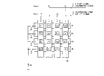
Flg. l shows an example of a driving method of
the device of Fig. 3 at n - 1. In Fig. 1, the
lnformation s~g~A~lq are lnputted to odd-numbered rows
of modulatlon electrodes and even-numbered ones
dlvlslonally two tlmes, and cut-off s1gnAls are
inputted to the l~ Ation elec~,odes to which no
~;. ~''i
- 14 ~ J~ 7 3 3
information signal is inputted. For example, the
voltage Vf necessAry for electron ~ 1 ssl on is Appl ~ e~
to the X2-th line of the eleo~on-emitting devices. For
inputting the information s1gnAls to the modulation
eleoL~odes (Yl, Y2, Y3, .... ), (1) flrstly information
slgnAls are inputted to Y2,~1-th ~ulAtion electrodes (m
- 0, 1, 2, ....) and cut-off S~gnA15 are lnputted to
Y2,~2-th - -lAtion ele~,odes, respectively, and (2)
then information signals are inputted to Y2~2-th
~~-l~tion ele~iodes and cut-off signals are in~ ed
to Y2.~-th modulation eleo~odes, respectively. Thereby
an electron beam em~ss1on pattern is formed
co~ ol~d~ ng to the information sl~nAls for the X2-th
llne. The above p~ocedu.e i8 COn~lCted 8~0ce881vely
for each of the ele~on-emitting device lines to form
an ele~lon be~ ~ l~s~n pattern for a picture image.
A picture image is fo~ ~' on an 1 ~e fG 1n~ by
irradiating the above electron beam . 1 8sl on pattern
thereon.
Fig. 2 shows another P - le where the value of
n is 2 in the device of Fig. 3. In Fig. 2, the
information signals are inputted diV~slo~Ally at
in~e~vals of two rows of ~ ~lAtion electrodes three
times. In each time, aut-off slgn~ls are inputted to
the modulation ele~odes to which information signals
are not inputted. For example, the voltage Vf for
electron emission is applied to X2-th line of the
,, : ~ , : . . .,,~ ,
,
.: , ,: . ,. : . . ~, . , . .. ,.. ~:
,. . ~ ... ......... . .. . .
- 15 - ~,112733
elec~lon-emitting devices. For inputting the
information s1gnals to the ~ tion electrodes, (1)
firstly information Stgnal~ are inpu~ed to Y3~l-th rows
of the ~-~ulation elec~Lodeg, and cut-off signals are
inputted to Y3,~2-th and Y3~3-th rows of ~ tion
elec~Lode~, respectively, and (2) then information
s~gnal~ are inpu~ed to Y3~2-th rows of ~ ation
electrodes and cut-off slgnAl~ are inputted to Y3,~1-th
and Y3~3-th rows of modulation ele~-odes, respectively,
and (3) finally information slgnals are inputted to
Y3~.3-th rows of ~ tion elec~ odes and cut-off
s~g~Al~ are inputted to Y3~1-th and Y3~2-th rows of
modulatlon eleu~ode~, ~e~eu~ively. Thereby elec~r~n
beam emission pa~e.-. 18 formed co ~es~oQdlng to the
information ~lgn~18 for the X2-th eleuL~on-emitting
device line. The above plocedu~e is cQnAucted
success~vely for each of the eleu~lon-emitting device
lines to form an eleu~on bo~ ~ ~sslon pattern for a
picture image. A picture image is formed on an image-
20 fo~ ~ ng ' ~ by irradiatlng the above electron beamsslon pattern thereon.
A suitable voltage is applied to the image-
forming member in order to irradiate effectively the ;
eleu~ on beam pattern emitted from the eleo~Lon source.
The magnitude of this voltage is suitably selected
Aep~ndlng on the ON voltage, the cut-off voltage, and
the kind of the electron-emitting device employed.
. . ~ s ; . ;. . ; : . - . . :
.: ,~ ' .'. !, . , ' '
. '' , ' ' ' ' ~ ~
i 7 3 3
- 16 - ~
- ' .
The afoLf -rtioned information signals (or
~ tion s~ 3n~ 1 ~ ) include an ON signal which allows
the irradiation of an electron beam onto the ~ ~ge
forming - ber in an amount of larger than a certain
level, and a cut-off st~n~l which shuts out the
irradiation of an elec~,ol~ beam onto the image-forming
- ~ . If gradation of the d1splay is desired, the
lnformation s~gnAls lnclude also gradation ~~na
which vary the quantity of the ele~-on beam
irradiation onto the ~ ~~e forming ~er ~he ON
~t~nAl and the cut-off signal are suitably selected
~6~ n~ on the klnd of the ele~,on-emitting device,
the voltage applled to the lmage-formlng member, and 80
~orth
The electron b r ~ene ating apparatus or the
~ fo ~ ~n~ appa~a~us which is driven a~cG,ding to
the drivlng method of the ~,~sen~ lnvention may
comprise a full-color lmage-formlng member ln which
fluorescent member of red (R), green (G), and blue (B)
are al,a,yed
Preferred examples of ~ ation means and -~
electron-emitting devices of the apparatus are -
descrlbed below in which the driving method o~ the
~.~sen~ inventlon ls sultably employed~
Flrstly, an example of a partie~ rly preferred
modulation means for the ele~-on-generating apparatus
and the image-fo- ~ ng apparatus is described below
2 ~ 3
- 17 -
Fig. 6 illu~trates an embo~ t in which
electron-emitting devices A and ~dul~tion electrodes 3
are both provided on one and the same face of a
substrate 1, and Fig. 7 illustrates ano~l-er embodiment
in which electron-emitting devlces A are provided on an
~n~ Ating subs~la~e I and -~l A, tion ele~L.odes are
laminated on the l~v~se face of the su~x~ a~e 1. In
these ~ s, electron-emitting device lines
having ~e~-~eu~lvely a plurality of elec~-on-emlttlng
reglons between wiring ele~lodeQ 2a, 2b, and
modulatlon ele~ odes 3 are a ~anged ln an XY matrix.
Fig. 8 shows an r hc'1ment callsd slmple matrix
~on~ c~lon gene.ally, ln whlch a plurality of
ele~on-emitting devices A are a r ~ anged in a matrix ~;
and each of the devices i8 ¢onn~cted with a 8~gnAl
wiring elec~de 3b and a scan-wiring ele~Lvde 3a.
The modulation means for any of the above three
ts does not require strlct posltlonal
regl~tratlon as that requlred ln the - ~lAtlon
ele~ode3 shown ln Fig. 3 be~/aon an ele~ ur,-emitting
region and an ele~lon pAQ~age open~ng 34, and
therefore does not cause irregularity of l~ ~nance in
luminous image like that c~Re~ by positional deviation
of the ele~lon pA~sAge open~ng from the eleo~-on-
emlttlng reglon.
In the devlces employlng the driving method ofthe present inventlon, the type of the electron-
... . . .. .. .
. ., ., - ~ . . . ~ . : . . .
. '
,
,, ~ , , .,: ~ .
, .. -.,:-.,
' - 18 - 21 1 ~33
emitting deviaes are not speclally llmited, but cold
cathode type devices are preferred. In the case where ~-
a plurality of hot ca~hodes are employed, uniform
ele~,on ~ 1ss~on characteri~tics in a large area are
not obtainable since elec~.on em1sslon characteristics
of the hot cathode are affec~ed by t Q ,)f rature
distribution. F~,LI.e" as the ele~,on-emitting
devices, surface con~uction type electron-emitting
devices are preferred in the present invention.
The surface ~,o~d~o~ion type ele~,on-emitting
devices are known, and is exemplified by a cold cathode
device ~1sclosed by M.I. ~11n~n, et al. (Radio Eng.
El~ Phys. Vol. 10, pp. 1290-1296 (1965)). Thls
devlce ut111 zeR the phenomenon that ele~o..s are
emltted from a thin film of small area fo -~ on a
e
substrate on Appl 1 cation of electric current in a
directlon parallel to the film face. The surface
co~d~lction type ele~,on-emitting device, ln addition
to the above-mentioned one ~1sclose~ by ~l~n~on et al.
employing SnO2(Sb) thin film, includes the one employing ~
an Au thin film (G. Dittmer: "Thin Solid Films", Vol. ~; -
9, p. 317 (1972)), the one emplo~ing an IT0 thin film ~ ~;
(M. Hartwell, and C.G. Fonstad: ~IEEE Trans. ED Conf.",
p. 519 (1983)), and so forth.
Flg. 9 illustrates a typical devlce
constitution of such surface con~uction type elec~lon-
emitting devices. The devioe in Fig. 9 comprises
2 i 12733
-- 19 --
elec~Lodes 22, 23 for electrlc connection, a thin film
25 formed of an elec~Lon-emittlng substance, a
substrate 21, and an ele~Lon-emitting region 24.
Convent~o~lly, in such a surface c~ndvction type
ele~.ol-emitting device, the electron-emitting region
is formed by a voltage A~pl~catlon treatment, called
~f~ 'ngn, of an emitting region prior to use for
electron ~ iss~on. The fo. ~ ng is a treatment of
flowing electric ~u.~ W-~o~l, the thin film 25 by
Appl~cation of a voltage bet e the ele~odes 22, 23,
~I.e e~y the emltting region-fo. ~ ng thin film being
oca~ly desL-oyed, defv -~, or denatured by the
n~ ated Joule'~ heat to form the ele~.o~-emittlng
region 24 ln a state of hlgh electric resl~ance.
Here, the state of hlgh eleatrlc resi~an~e means a
d~scs~t1nuol~c state of a part of the thln film 25 in
which ~ a_h~ having an "tslAnd ~-uu~u~a~ therein are
formed. The portlon of the thin film ln such a state
is spatially ~scontl n~nU~ but ls continuous
electrically. The surface conduQtion type electron-
emltting device emits ele~.ons, when voltage ls
Arpl~e~ ~e~.~een the elec~-odes 22, 23 to allow electric
~u e.~t to flow through the highly reslstant
~1~contlnuous fllm on the surface of the device
surface.
The lnventors of the p esen~ invention
d~sclose~, in Jar~nPse Patent Application Laid-Open
"
7 3 3
- 20 -
Nos. 1-200532 and 2-56822, a novel surface conduction
type electron-emitting device in which fine particles
~or emitting elec~-ons are ~1~pose~ in dlspersion
be~_r n ele~,odes. The inventors of the ~lesent
lnventlon later found that the above surface .;onduu~lon
type ele~lon ~ 1tting device is part1c~ ly eYce11ent
in the elec~.on : '8S~Qn eff1Q~ncy, the stability of
the emitted ele~,ons, and so forth, when the ~spersed
fine particles have an ave,a~e particle diameter in the
range of from 5 A to 300 A, and the intervals of the
fine particles are in the range of from 5 A to lO0 A.
. .'i
Such a type of surface con~ ion type ele~L,on-
emlttlng devlces havlng dls~e,~ed fine parti¢les have
~??ar.~c~es of (l) high ele~Gn em1ss1on efflciency,
(2) slmple structure and ease of productlon, (3)
poss~h11~ty of a-ran~ - ~ of a large number of devices
on one substrate, and 80 forth. Flg. lO shows a
, ~ . , .
typlcal device constitution of the surface conduotion
type electron-emitting device. In Fig. lO, the device
comprises devlce ele~,odes for electric co~eo~ion 22,
23, el6~,0n-emitting reglon 27 in whlch fine particles
26 for emitting elec~,o~s are disposed in dispersion,
and a substrate 21.
The present invention i8 described below in
more detail by refelence to Examples.
ExamPle 1
The device driven according to the present
. .
2~ 733
- 21 -
lnvention in this RYr le was an image-fo ~ ng
apparatus having surface condllction type electron-
emittlng devices and was driven as described below.
[Preparation r n~le of Image-F~_ 'ng Apparatus]
The ~ od for p.apa.a~ion of the lmage-fc_ 'ng
apparatus is ~Ypl~l n~ by reference to Figs. Il and 12.
(1) Device elec~lode~ 61a, 61b, and wiring
elea~.~des 62a, 62b were formed on a glass substrate as
the ~ n~Ul ating substrate 60. The eleoL-odes were
formed ~rom metallic nl~el in this r - le, but the
material therefor is not limited provided that it is
ele~ooo~ lve. The gap bet~ae.- the ele~,ode~ 61a,
61b was 2 ~m, and the pitch of the wirlng elec~odes
62a, 62b was 0.5 mm.
(2) Organic pAlla~lum (CCP-4230, made by Okuno
Seiyaku K.K.) was appl~ed bet e the elee~.~de3 61a,
61b, and the ~pl~ed matter was baked at 300~C for one
hour to form a fine partlcle ~ilm 63 ~ od of
palla~um oxlde.
(3) Above the substrate 60, the ~~ll~tion
ele~-odes 64 having ele~L,on pa~s~ge ope~lngs 65 were
placed and fixed in an XY matrix so as to be
pe-pend~c~ r to the wlring ele~L,odes 62a, 62b.
(4) A face plate 68 having a transparent elecL,ode
66 and a fluolesoen~ member 67 on its ln~lde faae was
pl~ced 4 mm above the subsL~a~e 60 by aid of a
supporting frame 69. Frit glass was applied to the
:. l .:
: , :
:. ' ' , ' ~' ' "'
..,
,
2 ~ , 7 3 3
- 22 -
Joint portion between the &~ppO~ ~ing frame 69 and the
face plate 68, and was baked at 430~C for more than 10
minutes.
(5~ The enolos~re prepared as above (constituted of
the substrate 60, the ~u~po,Ling frame 69, and the face
plate 68) was evacuated by a vacuum pump to a
sufficient v__ - dey~ee (preferably from 10-6 torr to ~
10-' torr). Then voltage pulse of a desired waveform ~ e
was Appl~e~ between the wiring ele~,odes 62a, 62b to
form elec~,on emitting reglon~ 70 bet~acn the device
eleu~,odes 61a, 61b. The pitch of the eleu~,on- ~ ;
emittlng region was made to be 0.5 mm. The fine
partloles ln the elec~,on-emlttlng region had an
~vu~a~a particle ~-r - ~e Of 100 A, and the ln~e~val
bet.le~r the partiales was 20 A accordlng to SEM
obse~vation.
The 1 ~e fo, 1 ng apparatus was prepared as
above whlch comprlses an eleu~ on source havlng
electron-emittlng devices a,,ar,ged ln a matrlx. With
this apparatus, at a voltage of from 5 to 10 kV applied
to the transparent eleo~,ode 66, cut-off con~ol was
practicable at a voltage of the ~ Ation electrode 64
of -30 V or more negatlve voltage; ON con~ol was
praot~c~hle at a voltage ~I.e~eof of zero volt or
h-gher; and gradatlonal ~-~P1AY was pract~oAh1s by
cont~nuo~cly changlng the quantlty of the electrons of
.
the emitted electron beam in the range of from -30 V to
' '' :~ ~
,
,
~ 273~
- 23 -
O V. In Fig. 11, the -- - al 71 denotes luminous spots
of the fluorescent b~ . -
[Example of Device-Driving Method]
The method of driving the device of the present
$nvention is explA~ne~ by refe,e-lce to Fig. 13 for the
case where ~aAnnlng is co~du~ed from the ele~ on- ~
emitting device line of MS1 ; ~-
(I) A coni~ant voltage is applied to the
~L~nQ~Arent elee~ode 66 (Flg. 11) by a voltage '~
application means (not shown in the drawing), and
ele~ ,on emlsslon voltage Vf i8 applied to the
elê~i~.on-emitting devlce llne (or i~cAnn1~ line) of
M-1.
(2) Of the information ~1gnAls for the g~Annln~
line of M-l, information 8~g~Al 8 to be inpu~ed to
even-numbered -lvlation ele~ odes (N - 2, 4, ....)
are s~o~ed in a memory 80, while the information
81~nA18 to be inpu~ed to odd-numbered ~ Ation -~
ele~,odes (N ~ 1, 3, 5, ....) are inputted directly
~he,eLo by a voltage Appllc~Ation means 81 as ~l~-lAtion
voltages (Vm1, Vm3, Vm5, ....) lncludlng ON voltages,
cut-off voltages and gradatlon voltages in
eio..~o~ldlng with the information slg~als. Durlng
this period, a cut-off voltage (V~) i8 applled to the
even-numbered modulatlon elec~odes (N ~ 2, 4, ....)
i,.e~ec~lvely of the lnformatlon 8~gnAl8 a~co,ding to
cut-off the s~gnals sent out from the slgnAl switching
,. ~ .
.. . ..
., ~ ,., '
' ' ' ' i ,, ' ' ' ;, ' ., ~ ~ ' ' .
'. . ., ~.. . ......
-.-- 2:1~273~
- 24 -
circuit (signal separation means) 82 to a voltage
application means 83.
(3) Then the s~gn~Al switching circuit 82 switches
the circuit so as to input, to the even-nl ~- ed ~;
modulation ele~ odes, the portion of the informatlon
sl~nAl~ for the soannlng line (M~ G~ed in the
- - y 80. Thereby ~ Ation voltages (Vm2, Vm~
....) including ON voltages, cut-off voltages and
, . , ,, ~ .
gradation voltages are lnpu~ed to even-n -~red
-~IlAtion ele.~,odes through the voltage Arplic~tion ~- ,
means 83 in corre~o~de~ce with the information
8lg~Al8. Durlng this perlod, a cut-off voltage (VO~
1~ ~pp~ed to the odd-numbered ~ ~lAtion ele~,odes (N
~ 1, 3, 5, ....) l,,e ~e ~lvely of the information
8~gnAl 8 acco,ding to cut-off the 8lgnAl~ sent out from
the ~1gnA~l switching circuit 82 to a voltage
Appl~cation means 81.
As described above, the p,oce~s of inputting
lnformation ~lgnAl~ of one soAnn~n~ llne in two steps
separately for odd-r- - ad - ~lation electrodes and
even-n~ -?red ones i8 cond~cted within the time of
sCAnn~ng of one llne of display.
The above steps of (1) to (3) are practiced for
each sCAnnlng line sequentially to ~lqplAy one or more
picture images on a fluorescent member face.
According to the driving method of this
Example, respective luminous spots fol ~ng an image
~; ? ; ~
,,; , ,, ~, ;",. ~ ,; ', " "~ : ., . '
~ 127~ -
- 25 -
~pl~y on the fluorescent - ?r face were e~ ly
uniform in size and shape, and gave e~t~ e~y fine and - -
sharp image without c os~alk.
The -' lAtion ele~L,vdes, which are a ny2d
in as ln Fig. ll in this r--~ le, may be the ones as ~ -
shown in Fig. 6, or Fig. 7. Wlth any ~ - t of the
~' l~tion ele~L~odes, a s~'lAr driving method as in
thls Example (Figs. 14 and 15) gave an image displayed
with spots of uniform and stable sizes and s~Ares with
high f1n~n~s without crosstalk. In the em~oAl r-ts of
Flg. 6 and Flg. 7, at an App~lcAtion voltage of the
L,~epArent eleo~,odas of from S to lO kV, the elec~,on
beam could be cut off at the modulation voltage of -40
V or more negative voltage, turned on at lO V or
hlgher, cont1m~o~ly con~,olled between -40 V and lO V
for gradational ~play.
ExamDle 2
The image-formlng apparatus ln this Example was
~,e~a~ed in the same - e as in r ~ e l e~ca~ that
the device ele.~,odes 61a, 61b and the wiring
ele~,ode~ 62 are a~,anged as shown ln Figs. 8 and 16,
modulation electrodes of Example l was not provided,
and fluorescent materials of red (R), green (G), and
blue (B) were a,,aryed in a black stripe constitution
as shown ln Fig. 18 such that one fluorescent materlal
(R, G, or ~) co,,e~pon~R to one elec~,on-emitting
device.
," , ~ ,, .," . ,,,;
2 ~ 7 3 3
- 26 -
In this wor~ing example, instead of such a
modulation eleo~,ode as used in Example 1, a s~gnal-
wiring ele~ode described later plays the same part as
.,.: ; :-,-,
the trAncpArent ele~ude does in R-r
. -. .
s tExample of Device-Driving ll~l.od]
The method of driving the device of the ~Le~en~
lnvention ls eYrl A1 ned by refe.ence to Fig. 17 for the -~
, ' : :
case where ~cAnn1ng is ~ondvcted from the eleo~-on~
emlttlng devlce line of M~
(1) A constant voltage is A~pl ~ ed to the
~ parent eleo~-ode by a voltage app~lcAtion means
(not shown in the drawing), and eleo~,~n emission
voltage Vf i8 A,rplled to the ele~ol. em~ton line (or
scAnn~o line) of M~1.
(2) of the infc -~lon 81gnAl8 for the sca
line of M-l, informatlon 8~nA18 to be inputted to
green-~sFl~ying signal wiring eleo~odes G and blue- ~ ;
~1~plAying 81Dn~Al wiring elec~odes B are ~G~ed in a
memory 80, whlle the lnformatlon 81gn~Al~ to be in~u~ed
to red-~playlng s~g~Al wiring ele~odes R are
inputted directly W-e~e~o by a voltage application
means 81 as ~ lation voltages (VmR) including ON
voltages, cut-off voltages and gradation voltages in
co.~e~yon~qnce with the information 8i~ 8. Durlng
this perlod, a cut-off voltage (VOtt) 18 applled to the
81gn~1 wlrlng electrodes G and B lrrespeotively of the
in~c- -~ion signals according to cut-off the s~gnal~
".,,, , , !,," .,~ :, , ,; . , ,; " ~ " " ", ~
~1~2733
"",
.: ...;:
sent out from the signal switching clrcuit 82 to a .
voltage application means 83.
(3) ~he signal switching circuit 82 switches the
circuit so as to input, to the slgnAl-wiring electrode
G, the portion of the information s~gnals ~Lo~ed ln the
~ ~_y 80 for the green-~lsplAying infG~ -Lion g1gnA~
of the scann~ng line of M=1, and ~d lAtion voltages
(VmG) including ON voltages, cut-off voltages and
gradation voltages are inpu~ed to the s~gnAl wiring
ele~L,ode G through the voltage A~pl1cAtion means 81 in ~.
cG-~e~o~d~noe with the information s1gnals. During
this perlod, a out-off voltage ~VO~) is applled to the
8lg~l-wiring ele~Lrodes R and B i~le~e~Lively of the
information stgnAls aoco,ding to cut-off the ~1g~Als
sent out from the s1gnAl switching circult 82 to the
voltage A~pl1c~tion means 83.
(4) The ~l~nAl switching circuit 82 switches the
circuit 80 as to input, to the s1gnAl-wiring ele~LLode
B, the portion of the infc_ ~Lion s1g~Als stored in the ~:
memory 80 for the blue-~ls~laying information s~gnA~ of
the sc~nn1ng line of M-l, and ~-lAtion voltages (VmB)
including ON voltages, cut-off voltages and gradation
voltages are il~puLLed to the ~lg~Al wiring electrode B
through the voltage Appl1catlon means 81 in
corre~po~snce with the information slgnals. During
this period, a cut-off voltages (VO~) is applied to the
s1gnAl-wiring eleo~-odes R and G irrespectively of the ~-:
, ,: ~, ~ ~ , :
~1 ~ 2733
- 28 -
information signals according to cut-off the sl gnal s ~ : ;
sent out from the s~n~l switching circuit 82 to the
voltage ~ppl~c~tion means 83.
As described above, the prooess of inputting
information s~gnals of one sc~nnlng line at intervals
of two ~1 gnAl -wiring elec~-odes in three steps for
three colors separately is oo~ c~ed within the time of
8CAnn1 n~ of one line of display.
As r~al~7e~ from the above descriptlon, the
application of the ~ tion voltage to the ~1 ~n~
wiring eleu~Lode in the p~esen~ working example
co~e~ dc to the ~ppl~cAtion of voltage to the
modulatlon elec~.ode in Example 1.
The above step~ of (1) to (4) are practiced ~or
each sc~nn1~g line slJcce~slvely to display a full-color
picture image on a fluorescent - ~-r faoe. '~
According to the driving method of this
Example, respective luminous spots formlng an image
~play on the fluorescent member faces of each color
were extremely unlform ln size and shape, and gave a
full-color image with imp~uved color purity with
eYcellent color repro~uc~b~lity without crosstalk.
The ~'-lation ele~L-odas, which are arranged
as in Figs. 8 and 16 ln this Example, may be arranged
as shown in Fig. 6, Fig. 7, or Fig. 11. Wlth any
~ ~Dd~ment o~ the modulation ele~odes, a slmllar
drlvlng method as in thls ~-~ le gave a full-aolor
' . ' ':; , ~ .; , ,
': ' ' ' ' ' . , ' ' :
'., " , ' , ', ' , ~ ~
,, : ' ' ' ' ' '
29 - ~112733
image with spots of uniform and stable slzes and sh~pes
with 1 .,loved color purity with eyoellent color
~eplod.lc~h11~ty and without ~-osx~alk.
The image-fc_ i ng apparatus of the present
invention will poss1hly be useful widely in public and
industrial application fields such as high-vision TV
picture tubes, cc ,-~er ~el Inals~ large-picture home
theaters, TV confelence YyYt - ~ TV telephc!ne ~y~t~
and so forth.
,
,, ,~