Note: Descriptions are shown in the official language in which they were submitted.
CFO 9685 ff3
21~~'~~~
- 1 -
1 Image Reading Device
BACKGROUND OF THE INVENTION
Field of the Invention
The present invention relates to an image reading
device adapted for use in an image information processing
apparatus such as a facsimile, an image scanner, a
copying machine or the like, and more particularly to an
image reading device and a photoelectric converting
element capable of converting optical signal not only of _:
visible spectral region but also of invisible spectral
region into electrical signal.
Related Background Art
In the field of image reading device, there are
already known a charge-coupled device (CCD), a I~iOS
device and an amplifying device formed by connecting a
capacitative load to the emitter of a phototransistor,
as disclosed in the U,S: Patent No. 4,791,469 granted to
the inventors T. Ohmi and N. Tanaka.
Also there are recently conceived various
applications, and image reading devices having novel
functions are being required.
For example the copying machine is required, in
addition to the improvement in image quality and the
color image reproduction, to have the ability to
recognize, reproduce and record an invisible image to
the human eyes.
v
Z~~~~~
- 2 -
1 An example of such invisible image is the image
formed with ink absorbing infrared light.
In general, the sensor for detecting the
invisible light is an individual device, and requires
a new design concept for effecting image detection,
in combination with a sensor for detecting the visible
light.
As a basic design concept, the present
inventors already found a technology of incorporating
a sensor for visible light detection and a sensor for
invisible light detection in a single semiconductor
chip. However, said technology still has a room for
improvement.
On the other hand, the image quality
improvement and the color copying capability of the
copying machine has brought the danger of forgery of
bandnotes, stamps, valuable securities etc, into
reality. For this reason, in the recognition of
banknote or the like, there have been devised various
methods such as detection of the stamp pattern on
the banknote.
Also utilizing the fact that the pattern of
the original image is formed with certain color hues,
the present applicant already proposed a method of
recognizing the banknote etc. from the color hue of
said original pattern.
Also certain banknotes enable recognition
2~.~. ~'~3
- 3 -
1 of the true one and the false one, by printing a
predetermined mark with fluorescent ink which emits the
visible light when irradiated with ultraviolet light.
Also for forming such predetermined mark, the
use of ink capable of absorbing the infrared light
was also proposed by the present applicant.
In such infrared light detecting device, the
Japanese Patent Application Laid-open No. 4-286350 of
which U.S. counterpart is U.S. Serial No. 139174
entitled "Image Processing Apparatus and Method
Therefore" filed on October 21, 1993 proposing
to achieve making compact of the device and easy optical
adjustment by a monolithic structure of a sensor for
ordinary color image formation and a sensor for infrared
light detection, thereby enabling to use a common
optical system.
However, such conventional system is difficult
to design in common for plural valuable securities,
because a visible pattern is the target of recognition.
Therefore, for distinguishing the valuable securities
of N kinds, it has been necessary to select the
features of N kinds in advance and to independently
recognize each security, and it has been difficult to
realize such apparatus inexpensively.
Also a CCD sensor for reading the images of
visible and infrared regions by separating the
spectral regions additionally requires, in comparison
r.
Z~~~~3
- 4 -
1 with the conventional sensor, an optical filter for
reading the infrared light and an increased number of
elements or lines of the sensor, whereby the sensor
itself and the post-processing system therefor become
complex and a decrease in the light-receiving area of
the sensor or an increase in the size of the sensor is
unavoidable.
Also, since the sensor elements for the
visible light and those for the infrared light are
arranged on a same plane, at least one of the sensors
may become out of focus, due to the difference in
the focus position.
Also in case of using such sensors for --
respectively reading the infrared information and
the visible information, it becomes necessary to
clearly separate the visible information and
other information.
Furthermore, for obtaining a satisfactory
resolving power on a monolithic CCD sensor over a wide
2p spectral range from visible to near-infrared region
or from visible to near-ultraviolet region, there is
required a significantly increased number of lenses,
leading to an increased cost and a larger space of
the device. Also in an optical system employing a
short-focus lens array, it has been impossible to
maintain a constant resolving power over a wide
spectral range, because such lens array is composed
- 5 -
1 of single lenses.
Also the conventional image reading device
employed in the office equipment such as copying machine
is composed for example of a CCD or a MOS sensor
requiring a long optical path, or a contact image
sensar.employing amorphous silicon, and such image
reading device is sometimes combined with color filters
for the color image reproduction.
However, such photoelectric converting device
combined with filters is not necessarily superior, in
terms of spectral sensitivity and resolving power for
infrared light detection, to the device for visible
light detection, and still has a room for improvement.
SUMMARY OF'THE' INVENTION
In consideration of the foregoing, the
object of the present invention is to provide a
compact image reading device capable of detecting the
optical signal over a wide spectral range from visible
to invisible region, and not giving much burden on the
designing of the optical system.
The above-mentioned object can be attained,
according to an embodiment of the present invention,,
by an image reading device in which the light-receiving
face of a first sensor for converting the optical signal
of the visible region into a first electrical signal and
that of a second sensor for converting the optical signal
~~~~'~3~
- 6 -
1 of the invisible region into a second electrical signal
are provided in different positions with respect to the
incident direction of light.
According to another embodiment, there is
provided an image reading device comprising reading
means in which the light-receiving face of a first
sensor for converting the optical signal of the visible
region into a first electrical signal and that of a
second sensor for converting the optical signal of the
invisible region into a second electrical signal are
provided in different 'positions with respect to the
incident direction of bight, image forming means for
forming an image based on said first electrical signal, --
discrimination means for effecting discrimination based
on said second electrical signal and a reference signal,
and control means for controlling the function of said
image forming means based on the output of said
discrimination means.
This embodiment enables highly precise image
reading over a wide spectral range, since the light-
receiving face of the visible light sensor and that
of the invisible light sensor can be independently
positioned at optimum conditions.
Still another embodiment of the present
invention provides an image reading device for secure
recognition of a specified original image.
Still another embodiment of the present
_
1 invention enables reading of the original image in the
visible light region and the infrared region,
inexpensively and securely in a simple configuration.
The above-mentioned object can be attained, in
said embodiments, by an image reading device provided
with means for recognizing that an object pixel is a
specified image, based on the image information ins.
the visible region and that in the infrared region, in
the position of the object pixel and in the positions
of the pixels in the vicinity, wherein the image
information of said visible region and:.infrared region
are read by common use of a same image reading sensor
or a part thereof, by switching an optical filter for ---
limiting the absolute light~.amount or a specified~~
spectral region.
Also there is provided an image reading device
provided with means for recognizing that an object
pixel is a specified image, based on the image
information in the visible region and that in the
infrared region, in the object pixel and in the pixels
in the vicinity, comprising a switchable optical
distance correcting filter for correcting the difference
in the focus position between said visible region and
infrared region.
Still another embodiment of the present
invention provides an image reading device capable of
satisfactorily reading the light of visible region and
,::
21~~'~~u
-8-
1 that of an invisible region.
The image reading device of this embodiment
comprises a filter for intercepting the invisible
light only between a sensor for reading the visible
information and the original image, in reading the
visible and invisible information by focusing on a
solid-state image sensors formed in.vmonolithic manner
on a same substrate.
Also there is provided means for correcting
the difference in focus position between the visible
and invisible information, in reading the visible and
invisible information by focusing on a solid-state
image sensors formed in monolithic manner on a same
substrate.
Still another embodiment of the present
invention provides a photoelectric converting device
improved in spectral sensitivity and resolving power.
According to this embodiment, there is
provided a photoelectric converting device for
converting the optical signal of infrared region into
an electrical signal, comprising a photoelectric
converting element for converting the optical signal of
visible region into an electrical signal, and infrared-
visible light conversion means for selectively
generating an optical signal of visible region to
irradiate said photoelectric converting element, based
on the optical signal of infrared region.
2~.~?'~3a
- 9 -
1 An electrical signal improved in spectral
sensitivity and resolving power can be obtained by
detecting the visible light generated according to the
intensity or the presence or absence of the infrared
light, instead of the conventional selective detection
of the infrared light within a wide spectral range
covering from the visible to infrared region.
BRIEF DESCRIPTION OF THE DRAWINGS
Fig. 1 is a schematic cross-sectional view of
an embodiment 1-1 of the image reading device of the
present invention;
Fig. 2 is a chart showing spectral characteristics
of color filters to be employed in the present invention;
Fig. 3 is a chart showing spectral characteristics
of a visible light cut-off filter to be employed in the
present invention;
Fig. 4 is a chart showing light emission
characteristics of a light source to be employed in the
present invention;
Figs. 5A and 5B are schematic views of the
embodiment 1-1 of the image reading device of the presen t
invention;
Fig. 6 is a schematic view of a pixel of the
embodiment 1-1 of the image reading device;
Fig. 7 is a chart showing spectral
characteristics of infrared absorbing paint to be
,~'"''''.
-lo-
1 employed in the present invention;
Fig. 8 is a chart showing spectral
characteristics of a far-infrared cut-off filter to be
employed in the present invention;
Figs. 9A and 9B are schematic views of an embodiment
1-2 of the image reading device of the present invention;
Figs. l0A and lOB are schematic views of an embodiment
1-3 of the image reading device of the present invention;
Fig. 11 is a schematic view showing an example
of the image information processing apparatus of the
present invention;
Fig. 12 is a schematic view of an original
image to be read by the image reading device of the
present invention;
Fig. 13 is a schematic view showing the reading
operation of the image reading device of the present
invention;
Fig. 14 is a block diagram showing a signal
processing unit of the image reading device of the
present invention;
Fig. 15 is a block diagram of an edge enchancing
circuit of the image reading device of the present
invention;
Fig. 16 is a schematic view of a pixel data
map:
Fig. 17 is a schematic view of a part of the
original reading unit in an equal-size optical system
~1~27~~
- 11 -
1 in an embodiment 2-l;
Fig. 18 is a schematic view of a full-color
copying machint in the embodiment 2-l;
Fig. 19 is a block diagram of the embodiment;
Fig. 20 is a flow chart of the control sequence
of the embodiment;
Figs. 21A and 21B are magnified views of the
light-receiving elements of the CCD sensor in the
embodiment 2-1;
Fig. 22 is a chart showing the spectral
Sensitivity characteristics of the CCD sensor in the
embodiment;
Fig. 23 is a chart showing the spectral
transmittance of the near-infrared absorbing ink
employed in said embodiment;
Fig. 24 is a chart showing the spectral
characteristics of the original illuminating lamp
employed in the embodiment;
Fig. 25 is a chart showing the spectral
characteristics of the far-infrared cut-off filter
employed in said embodiment;
Fig. 26 is a chart showing the spectral
characteristics of the visible cut-off filter employed
in the embodiment;
Fig. 27 is a chart showing the spectral
characteristics of the infrared cut-off filter
employed in the embodiment;
Fig. 28 is a schematic view showing the vicinity
~.-. ~1~~'~~~
- 12 -
1 of the lens and the CCD sensor in a reduction optical
system in an embodiment 2-2;
Fig. 29 is a view showing the structure of a
full-color copying machine in the embodiment 2-2;
Fig. 30 is a view showing the structure of the
CCD sensor in the embodiment 2-2;
Fig. 31 is a schematic view showing the vicinity
of the lens and the CCD sensor in a reduction optical
system in an embodiment 2-3;
. Fig. 32 is a view showing an example of the
pattern in the embodiment;
Fig. 33 is a view showing the method for
discriminating a specified original in the embodiment;
Fig. 34 is a block diagram of the hardware
realizing the discriminating algorithm of the
embodiment;
Fig. 35 is a view showing the state of detecting
the identification mark of a copy.-inhibited original,
in an embodiment 3-1;
Fig. 36 is a view showing the structure of a
color copying apparatus employing the present invention;
Fig. 37 is a chart showing the spectral
characteristics of the filter positioned immediately
after the original illuminating lamp in the embodiment;
Fig. 38 is a chart showing the spectral
characteristics of the original illuminating lamp
employed in the embodiment;
2~~~'~3~
l~ -
1 Figs. 39A and 39B are views showing the structure
of the CCD sensor employed in the embodiment;
Fig. 40 is a chart showing the spectral
sensitivity characteristics of the CCD employed in
the embodiment;
Fig. 41 is a chart showing the spectral
characteristics of the infrared cut-off filter employed
in the embodiment;
Fig. 42 is a chart showing the spectral
characteristics of fluorescent light in the embodiment;
Fig. 43 is an external view of the CCD sensor
in an embodiment 3-2;
Fig. 44 is an external view of the CCD sensor
in an embodiment 3-3;
Fig. 45 is a view showing the equal-size
optical system in an embodiment 3-4;
Fig. 46 is a view showing the structure of
the CCD sensor employed in the embodiment;
Fig. 47 is a chart showing the axial chromatic
2Q aberration of the reading lens;
Fig. 48 is a view showing the shape of the CCD
cover glass employed in an embodiment 3-6;
Fig. 49 is an external view of the element for
optical path splitting and optical length correction
employed in the present invention;
Fig. 50 is a magnified view of the reading unit;
Fig. 51 is a chart showing the spectral
~~.~<.;'~3~
- 14 -
characteristics of the element;
Fig. 52 is a view showing the structure of a
color copying apparatus;
Fig. 53 is a chart showing the distance between
the optical path correcting mirror and the half mirror
and the distance of separation between the visible and
infrared lights as a function of the light incident
angle;
Fig. 54 is a chart showing the spectral
1S characteristics of the dichroic mirror;
Fig. 55 is a schematic cross-sectional view
of an example of the photoelectric converting device of
the present invention;
Fig. 56 is a schematic cross-sectional view of
15 another example of the photoelectric converting device
of the present invention;
Fig. 57 is a spectral chart showing the
infrared exhausting effect; and
Fig. 58 is a schematic cross-sectional view
20 of the photoelectric converting device of the present
invention, utilizing the infrared exhausting effect.
DETAILED DESCRIPTION OF THE PREFERRED EMBODIMENTS
The image reading device of the present
25 invention is featured by a fact that the light-
receiving face of the sensor for visible light and that
of the sensor for invisible light are made respectively
"""'~ 2~.~~'~36
- 15 -
1 different for the direction of the incident light, but
the planar positions (positions in a plane perpendicular
to the incident direction) of said sensors are not
particularly limited. However, in case of a line:~.sensor,
the sensor array for visible light and that for invisible
light are preferably constructed as separate lines.
Also in the sensor array for visible light, the sensor
elements for red (R), green (G) and blue (B) or the
sensor elements for yellow (Y), cyan (C) and magenta (M)
may be positioned in an in-line arrangement or may be
arranged to constitute three parallel lines.
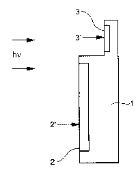
Fig. 1 is a schematic cross-sectional view of
the image reading device of the present invention,
wherein a sensor 2 for visible light has a light-
receiving face 2' which is different from that 3' of
a sensor 3 for invisible light.
The photoelectric converting elements (sensor
elements) constituting the~~light-receiving face of the
present invention are advantageously composed of
photo-voltaic elements or photoconductive elements
such as photodiodes or phototransistors. The
photoelectric converting elements for converting the
optical signal of the visible region into the electric
signal may be constituted by the elements composed
of a material capable of selectively absorbing the
optical signal of the visible region only, or by the
elements provided with a filter capable of
~1~~''~~~
- 16 -
1 transmitting the light of visible region but
intercepting the light of a spectral region to be
utilized for photoelectric conversion in other
photoelectric converting elements, among the invisible
region.
More specifically, for obtaining a black-and-
white signal, there is attained selective sensitivity
in the visible wavelength region from 400 to 700 nm,
by selecting the material constituting said elements
or by providing the elements with a filter selectively
transmitting the light of the above-mentioned wavelength
region. Also the optical signal of a specified region
within the visible spectral region may be obtained by
constructing said elements with a material selectively
having sensitivity in said specified region, or by
providing the elements with a filter capable of
transmitting the light of said specified spectral
region.
Also for obtaining color signals, such as of
red (R), green (G) and blue (B), there are employed
elements of plural kinds, consisting of elements (R
elements) having selective sensitivity in the R region
(spectral region for example from 580 to 700 nm),
elements (G elements) having selective sensitivity in
the G region (spectral region for example from 480 to
580 nm), and elements (B elements) having selective
sensitivity in the.,B region (spectral region for
2 :~ ~ ~ '~ ~ i
- :17 _
1 example from 400 to 480 nm).
Also in this case, there may be employed
elements composed of materials having selective
sensitivities in, namely capable of selectively
absorbing the lights of the above-mentioned R, G and
B regions, or provided elements having sensitivity in
all the R, G and B regions with filters selectively
transmitting the lights of said R, G and B regions
respectively.
Alternatively, a position of a semiconductor
junction such as a PN junction of the photodiode or
the phototransistor may be varied to obtain a
selective sensitivity.
Fig. 2 is a chart showing the representative
spectral characteristics of the light transmitted by
the filters, wherein the relative sensitivity in the
ordinate corresponds to the transmittance for the
visible light. In case the elements are given the
selective sensitivities by the selection of the
constituting materials, the elements are formed with
the materials having the light absorbing characteristics
corresponding to the relative sensitivities shown in
Fig. 2.
In the present invention, any of the visible
and invisible spectral regions, and the R, G and B
spectral regions are not clearly distinguished by the
wavelength, but the photoelectric converting elements
p
- 18 -
1 to be employed therein need only to be so constructed
as to photoelectrically convert the ultraviolet, blue,
green, red and/or infrared lights by a necessary amount
and substantially not to convert the unnecessary lights,
in order to obtain the required signals.
On the other hand, for converting the optical
signal of the invisible spectral region into the
electrical signal, there are employed cphotoelectric
converting elements having selective sensitivity for
example for the ultraviolet light or the infrared light.
Also in this case there may be employed elements composed
of a material having selective sensitivity in said
invisible spectral region, or elements composed of a
material having sensitivity in a wide spectral range
including said invisible spectral region, composed with
a filter having selective transmittance for the light
of said invisible spectral region.
Fig. 3 is a chart showing representative
spectral characteristics of the above-mentioned filter,
wherein the relative sensitivity in the ordinate
corresponds to the transmittance for the invisible
light. There is shown an example of filter having
selective sensitivity in the infrared region (wavelength
region for example above 750 nm), but such example is
not limitative.
The solid-state image reading device of the
present invention may be constructed as a color line
~~~.~'~3 i
_ Z9
1 sensor as shown in Fig. 1, in which the elements for
visible light and those for invisible light are
periodically arranged in mutually separate lines.
Preferably it is so constructed that a pixel in terms
of the resolving power of the color signal contains
an element (R element) having selective sensitivity
in the R region, an element {G element) having
selective sensitivity in the G region, an element
(B element) having selective sensitivity in the B
region, and an element (IR element) having selective -
sensitivity in the invisible region.
The optical signal to be detected may be
generated from a three--dimensional image or a two-
dimensional image, and a representative example of
said two--dimensional image is a flat image such as
an original document. Consequently, in case of use in
a system for reading the image of an original
document, there is preferably provided illumination
means for illuminating the original. Such illumination
means may be composed for example of a light-emitting
diode, a xenon lamp or a halogen lamp. Fig. 4 shows
representative light emission spectral characteristics
of the light source. However the light source needs
only to emit the light of a spectral region required
corresponding to the optical signal to be detected,
and is not limited to that having the characteristics
shown in Fig. 4. A light source emitting the light of
211~'~~~
- 20
1 the characteristics shown in Fig. 4 can at least
provide the light in the R, G and B regions and the
infrared light in the invisible spectral region.
In the following there will be explained
embodiments of the present invention, but it is to be
understood that the present invention is not limited to
these embodiments but can be realized in any form
attaining the objects of the present invention.
(Embodiment 1-1)
Fig. 5A is a plan view, seen from above, of
a CCD ~ serving as the image reading device, and Fig.
5B is a cross-sectional view thereof.
The CCD 1 is composed of a first element
array 100 and a second element array 101.
In the first element array 100, the elements
are cyclically provided with R filters 102, G filters
103, and B filters 104, formed by evaporation, in the
order of R, G, B, R, G, 8,..., thereby constituting a
reading system in which a pixel 105, consisting of a
set of three elements of R, G and B, constitutes a
minimum reading area.
The filters provided by evaporation on
respective elements have the spectral characteristics
as shown in Fig. 2.
On the other hand, in the second element array
101, the elements are arranged with a pitch equal to
three times of the pitch of the elements in the first
- :2 ~. --
1 element array 100. Stated differently, the element
pitch of the second array 101 is same as the pixel
pitch of the first element array 100.
The second element array 101 is provided, by
evaporation, with a visible light cut-off filter of the
characteristics shown in Fig. 3, so that the light
components less than 700 nm are cut off and the element
array 101 can read the infrared component.
Also, as shown in Fig. 5B, the second element
' 10 array 101 has a step difference d of 300 um to the first
element array 100, for obtaining a longer optical path.
This is because the focal length of the optical system
varies depending on the wavelength, and the image
becomes out of focus for the infrared light unless the
optical path is made longer.
Fig. 6 shows the dimension and the positional
relationship of the elements of the first element array
100 and the second element array 101. It is assumed
that the reading unit has a resolving power of 400 dpi
and that, for the purpose of simplicity, an equal-size
optical system is employed.
For realizing the resolving power;of.400 dpi,
the minimum reading area becomes 63.5 x 63.5 um.
Consequently the size of the R, G and B elements becomes
21.1 x 63.5 um, while the TR elements becomes 63.5 x
63.5 um. The distance between the first and second
element arrays is selected as 127 um. Stated differently,
~~.~r~'~3 ~
- 22 -
1 said arrays are separated by a distance corresponding
to twice of the array 100 or 101.
The signals read by the arrays 100, 101 are
so controlled as to be transmitted to a signal processing
unit 211.
(Embodiment 1-2)
In this embodiment, the element array 101 can
read the signal in a spectral region exceeding 700 nm,
but the infrared absorbing paint has a spectral
distribution having an extremely narrow band width,
with a~peak at 800 nm, as shown in Fig. 7.
However, depending on the light source to be
employed, there may be provided enough energy even in a
region exceeding 1000 nm.
If such light source is employed, the
discrimination of absorption becomes difficult because
of the unnecessary energy above 800 nm. For this
reason, the element array 101 is preferably provided
with a far infrared cut-off filter of the characteristics
as shown in Fig. 8.
Said far infrared cut-off filter may be provided
in any position in the optical path, because, in the
element array 100, the far infrared light is already
cut off by a filter evaporated on the surface of the
elements.
For example, acid filter may be conveniently
positioned in front of or behind a lens 209, because
~"~,,,~
~1~~'~3~
- 23 -
1 the filter can be easily replaced when the fluorescent
characteristics of the fluorescent paint to be printed
on the original document is varied.
(Embodiment 1-3)
In the foregoing embodiments, the color sensor
is constructed as shown in Figs. 5A and 5B. In the present
embodiment, the substrate of the CCD is formed in an
inclined shape as shown in Figs. 9A and 9B, in such a manner
that the first line 100 and the second line 101 has a
optical path difference d of 300 um.
In this manner the visible optical signal and
the infrared optical signal are both in focus, so that
the precision of discrimination becomes improved.
Also as a variation of this embodiment, a
similar effect can be obtained by placing planar CCD
sensors in an inclined position.
(Embodiment 1-4)
In this embodiment, a color sensor consisting
of an array 171 having sensitivity to blue, an array
172 having sensitivity to green, an array 173 having
sensitivity to red and an array 174 having sensitivity
to infrared region is given step differences, matching
the focal positions of respective colors. There are
preferably provided a step difference dl of 20 um between
B and G, a step difference d2 of 50 um between G and R,
and a step difference d3 of 280 um between~~,R and IR.
These values depend on the optical system to be
2~.1~'
24 ~-
1 employed, and are preferably optimized according to
each optical system.
The presence of four CCD lines requires phase
matching of all the color signals with a FIFO memory.
Also as modifications of this embodiment, it
is possible to form the substrate in inclined manner
or to place a planar sensor in inclined manner.
In this manner the visible optical signal and
the infrared optical signal are both in focus, so that
the precision of discrimination can be improved.
Also the distance between the array of the
infrared component reading elements and the array of
the visible component reading elements, selected as an
integral multiple of the resolving power of the reading
system, enables electrical compensation of said
difference for example by a line buffer, and
facilitates comparison of the signals from the two
element arrays which read a same image area. It is
furthermore possible to dispense with said line buffer,
by utilizing the FIFO memory for example in an edge
enhancing circuit.
(Image Information Processing Apparatus)
In the following there will be explained a
representative example of the image information
processing apparatus equipped with the image reading
device, according to any of the foregoing embodiments
of the present invention.
~~~~7~s
- 25 -
1 (Structure of Image Scanner Unit)
In Fig. 11 there are shown an image scanner unit
201 for reading the original image and effecting digital
signal processing, and a printer unit 202 for printing
a full-color image on a sheet, corresponding to the
original image read by the image scanner unit 201.
In the image scanner unit 201, there is
provided a mirror-surface thick plate 200. An original
204 placed on an original supporting glass (hereinafter
called platen) 203 is illuminated by a halogen lamp
205, and the reflected light from the original is focused,
by a lens 209, on said color sensor 1 serving as the
image reading device, whereby the full-color signals of
the red (R), green (G), blue (B) and infrared (IR)
components are supplied to a signal processing unit 211.
A reading unit 207 is mechanically moved, with
a velocity v, in a perpendicular direction (hereinafter
called sub scanning direction) to the electrical
scanning direction (hereinafter called main scanning
direction) of the color sensor, thereby scanning the
entire surface of the original.
The signal processing unit 211 electrically
processes the read signals to separate the components
of magenta (M), cyan (C), yellow (Y) and black (BK),
for supply to the printer unit 202.
(Structure of the Printer Unit)
The image signals M, C, Y, BK supplied from
,.
2
- 2'6 .-
1 the image scanner unit 210 are supplied to a laser driver
212, which in~.;response modulates a semiconductor laser
213. The laser beam emitted therefrom is guided through
a polygon mirror 214, an f-8 lens 215 and a mirror 216
and scans a photosensitive drum 217.
A rotary developing unit 218 is composed of a
magenta developing unit 219, a cyan developing unit 220,
a yellow developing unit 221 and a black developing unit
222, which in turn come into contact with the photosensitive
drum to develop the electrostatic latent images of M, C,
Y and BK formed on the photosensitive drum 217 with
corresponding toners.
A sheet supplied from a sheet cassette 224 or
225 is wound on a transfer drum 223, and the toner images
developed on the photosensitive drum 217 are transferred
onto said sheet.
After the successive transfers of the four color
images of M, C, Y and BK in this manner, the sheet is
discharged through a fixing unit 226.
In the foregoing there has been briefly
explained the structure of the scanner unit and the
printer unit principally constituting the apparatus,
and in the following there will be given a detailed
explanation on the image scanner unit 201.
(Original)
Fig. 12 shows an original 630 on which a
pre-registered pattern 631 is printed with infrared
,,
- 27 -
1 absorbing paint.
In addition to the pattern 631, characters and
images 632 are printed with ordinary ink on the
original 630.
The printed infrared absorbing paint, absorbing
the infrared light having wavelength in excess of 700 nm,
appears almost colorless to the human eyes sensitive to
a spectral region of 400 - 700 nm, and is therefore
extremely difficult to recognize.
The spectral characteristics of said infrared
absorbing paint is same as shown in Fig. 7.
The amount of the above-mentioned infrared
absorption can be detected by cutting off the visible
light component and extracting the infrared light
component only by the element array 101 in the sensor 1.
(Pre-scan)
The image scanner unit 201 effects a pre-scan,
as a pre-treatment before the copying of the original
630, as will be explained in the following.
At first the lamp 205 illuminates a white
shading plate 640, fixed in a part of the platen 203 as
shown in Fig. 13.
The reflected image of said white shading plate
640 is focused, through the lens 209, onto the CCD 210.
The image of the white shading plate 640, read
by the element arrays 100, 101 of the sensor 1, is
processed in the signal processing unit 211, and the data
z~.~~"'~3~
_ 28 _
1 for compensating the unevenness in the illumination by
the lamp 205, and the data for compensating the
unevenness in the sensitivity of the element arrays
100, 101 of the sensor 1 are prepared and are stored
for respective arrays.
Subsequently the reading unit 207 is mechanically
moved in a direction m with a velocity v by an
unrepresented driving system, thereby scanning the
entire surface of the original. In this operation, the
signal processing unit 211 extracts the maximum and
minimum values of the original density, from the image
of the orig~.nal 630 read by the element array 100 of
the sensor 1, and calculates the print density at the
copying operation.
Thereafter the reading unit 207 is mechanically
moved in a direction n shown in Fig. 13 with a velocity
v by the unrepresented driving system, for returning to
the reading start position, or, the home position.
(Copying of Original and Pattern Detection)
After the preparation of the above-mentioned
shading correction data, the reading unit 207 returns to
the home position and starts the reading of the original
630. At the same time there is detected whether the
original 630 has the pattern 631.
The presence or absence of the pattern is
discriminated by the comparison of the information
read by the element array 100 of the sensor 1 and that
z~~~~~~
- 29 -
1 read by the element array 101.
More specifically, the image reading for image
reproduction is conducted by the element array 100,
while the image reading for detecting the pattern 631
is conducted by the element array 101.
In the following there will be given an
explanation on the signal processing unit 211 for
processing the read signals. The block diagram of said
unit 211 is shown in Fig. 14.
At first there will be explained the signal
processing system for the element array 100.
The analog image signals released from the
element array 100 are entered, in the order of R, G
and B and in synchronization with the drive signal for
the sensor 1, simultaneously to three sample-hold
circuits 121a - 121c. The sample hold circuit 121a
generates a sampling signal at the timing of entry of
the R signal, and is capable of retaining the analog
level of the sampled signal until a next R signal is
entered.
Similarly the sample-hold circuit 121b
generates a sampling signal at the timing of entry of
the G signal and the sample-hold circuit 121c generates
a sampling signal at the timing of entry of the B
signal.
As a result, the sample-hold circuits 121a -
121c respectively release the R, G and B signals, which
~~~.2'7~~
- 30 -
1 are respectively supplied to A/D converters 122a - 122c,
wherein the analog image signal is converted into an
8-bit digital image signal. The obtained digital
signals are supplied to shading correction circuits
124a - 124c, for being subjected to shading correction.
The shading correction has already been explained
in relation to the pre-scanning, and the correction data
for R, G and B colors prepared therein are stored in a
RAM 123.
During the image reading, the correction data
for each element are supplied from the RAM 123 to the
shading correction circuits 124a - 124c, thereby
correcting the read data.
The image signals released from the shading
correction circuits 124a - 124c are supplied to a
5 x 5 edge enhancing circuit 125, which emphasizes the
contour of the read image in the following manner.
Fig. 15 shows the structure of said edge
enhancing circuit 125. The edge enhancement is
conducted for each of the R, G and B colors, but Fig.
15 shows the circuit for one color only. Naturally
other two circuits have the identical structure.
In Fig. 15 there are provided FIFO memories 131
- 134 each having a capacity capable of retaining the
data of a line in the element array 100 of the CCD
210.
The four FIFO memories are connected as shown
i
''' ~1~~'~3J
- 31 -
1 in Fig. 15, so that, when the pixel data of an n-th
line are entered to the FIFO 131, the FIFO memories
131, 132, 133, 134 respectively release the data of an
(n - 1)-th line, an (n - 2)-th line, an (n - 3)-th line
and an (n - 4)-th line.
The input signal and the output signals of the
FIFO memories 131 - 134 are supplied to a delay circuit
135.
Said delay circuit 135 is provided with several
pixel delaying circuits for the entered signal of m-th
pixel, thereby providing an arithmetic operation circuit
136 with the pixel data of the (m - 1)-th, (m - 2)-th,
(m - 3)-th and (m - 4)-th pixel as well as the m-th
pixel. Thus the circuit 136 receives the data of 25
pixels in total.
Fig. 16 shows the map of the entered data.
Thus the operation unit 136 receives the data of the
surrounding 24 pixels together with the data of a
hatched object pixel.
The operation unit 136 multiplies the data of
the object pixel by 25, and subtracts the data of the
surrounding pixels.
Thus, if the data of the object pixel is larger
than the data of the surrounding pixels, the data of the
object pixel becomes even larger, and vice versa.
This process increases the contrast of the
contour of the image, thus enhancing the reproduced
- 32 -
1 image.
The edge enhanced image data are supplied,
through a logarithmic conversion unit 127 for effecting
luminance-density conversion, and a masking conversion
unit 128 for effecting optimum correlated color
correction, to the printer unit.
In the following there will be explained the
signal processing system for the element array 101.
Although it is basically same as that for the element
array 100, but the edge enhancing circuit is eliminated
because the image reproduction is not the object.
The data released from a shading correction
circuit 124d are supplied to a signal comparison circuit
126.
Other input data are obtained from the edge
enhancing circuit, but, as will be apparent from Fig. 6,
the object pixel in the edge enhancing circuit is
present on the (n - 2)-th line.
The comparison of the data of the arrays 100,
lOl would require a line buffer for compensating the
distance of two lines as shown in Fig. 6, but the edge
enhancement on the data of the array 100 provides the
data corresponding to a same position on the original.
The signal comparison circuit 126, serving as the
discrimination means, compares the image data of the
arrays 100, 101 and sends the result of comparison to
an unrepresented CPU.
2~12~3~
- 33 -
1 In the signal comparison, it is to be noted
that the printing ink of a high density and a low
saturation tends to contain pigment of carbon black
family, and such ink, absorbing the infrared light, has
to be separated from the information to be discriminated.
In the present embodiment, therefore, whether
the IR absorption pattern corresponds to the pattern to
be discriminated is identified by the comparison of the
minimum value K of the R, G and B signals and the IR
signal in the following manner:
X = IR - const. x min(R, G, B).
More specifically, the value X is determined
for each pixel and is cumulatively added for the
entire original, and when the cumulative value reaches
a predetermined reference level, the unrepresented
CPU functions as the control means for the image
forming operation and controls the printer unit so as
to immediately interrupt the copying of the original.
There can be conceived certain variations in
the image information processing apparatus explained
above.
For example the line position correction for the
element arrays 100, 101 need not necessarily utilize the
FIFO memories of the 5 x 5 edge enhancing circuit, but
may instead utilize the FIFO memories for example of the
error diffusion process.
Also the pattern discrimination is not necessarily
~ :~ ~. ~ '~ '~ i
- 34 -
1 limited to the signal comparison in the signal
comparison circuit but may rely on pattern matching
according to the image shape extracted by the signal
comparison, in order to control the original copying
operation. In this case there is required a large and
complex pattern matching circuit, but, as the kind of
the original can be identified from the pattern shape,
there is enabled such control as to authorize the
copying operation for certain originals in response to
the entry of a password, but to prohibit the copying
operation for other originals.
This embodiment enables precise detection of the
optical signal with a wide dynamic range and over a wide
spectral range, without complicating the optical system.
(Embodiment 2-1)
The following embodiment shows an application of
the present invention to a copying apparatus, but such
application is not limitative and the present invention
is naturally applicable to various other apparatus,
such as an image scanner connected to a computer.
Fig. 18 shows the structure of an embodiment 2-1
of the device of the present invention, wherein an image
scanner unit 1101 effects original reading and digital
signal processing, and a printer unit 1202 for printing
a full-color image on a sheet, corresponding to the
original image read by the image scanner unit 1101.
,.
2~, ~.~~3;~
- 35 -
1 (Image Scanner Unit)
Fig. 17 is a schematic view show-ing a part of
the original reading unit of the equal-size optical
system of said image scanner unit 1101, provided with a
mirror-surface pressure plate 1100. An original
document 1104 placed on an original supporting glass
(hereinafter called platen) 1103 is illuminated by a
halogen lamp 1125, of which spectral characteristics
are shown in Fig. 24, and the reflected light from the
original is supplied to a lens array 1122 and is
subjected to the cut-off of a spectral region above
about 850 nm by a dichroic filter 1130 of which the
spectral characteristics are shown in Fig. 25. Then
by means of switchable filter means provided on a
horizontally movable stage 1128, the image of the near-
infrared region around a wavelength of 800 nm or the
image of the visible spectral region of 400 - 700 nm
is selectively supplied to a CCD line sensor for image
reading. Said stage 1128 is driven by a laminated
piezoelectric actuator 1129 and selectively moves in
the lateral direction in Fig. 17. On said stage 1128
there are mounted a filter 1123 of which the spectral
characteristics are shown in Fig. 26, and a near-
infrared cut-off filter 1124 of which the spectral
characteristics are shown in Fig. 11, and said stage
1128 is so moved that the filter 1123 or 1124 is
inserted between the lens array 1122 and the sensor
N.~~ '~~J~
- 36 -
1 1121 respectively at the image reading in the near-
infrared region or that in the visible region. On
said filter 1124 there is provided a glass plate 1127
for compensating the difference in image positions
between the near-infrared light and the visible light
in this embodiment 2-1,
Figs. 21A and 21B show the structure of the
sensor 1121 employed in the present embodiment.
The sensor 1121 is composed of a single
1.0 photosensor element array, in which the photosensor
elements are provided with evaporated filters of R, G
and B colors which are cyclically arranged in the order
of R, G, B, R, G, B.., thereby constituting a reading
system in which a pixel consisting of a set of R, G
15 and B photosensor elements is the minimum reading area.
The spectral characteristics of said filters are
shown in Fig. 22. The elements equipped with the R
filter are sensitive also to the invisible spectral
region above 700 nm, and are capable of satisfactory
20 image reading in the near-infrared region around 800 nm,
by the use of the filter 1123 and the dichroic filter
1130. For the photosensor elements having the G or B
filter the relative sensitivity above 700 nm is not
shown, because the data from said photosensor elements
25 are used only for the image reading in the visible
region. In fact the relative sensitivity above 700
nm can be considered as almost zero in the image
2~~2'~3~i
- 37 -
1 reading in the visible region, because the
aforementioned near-infrared cut-off filter 1124 is
used in the image reading in the visible region.
In order to realize a resolving power of 400
DPI (dots per inch) with this sensor, the minimum
reading area should be of a size of 63.5 x 63.5 um.
Consequently, the R element 152, G element 153 and B
element 154 should be of a size of 21.1 x 63.5 um each.
Also the image reading in the IR region utilizes the R
elements, so that the reading area becomes 21.1 x
63.5 um.
The image data focused on the sensor 1121 are
supplied, in the form of the red (R), green (G) and
blue (B) components of the color information, to a
signal processing unit 1198. The original scanning
unit 1111 is mechanically moved with a velocity V, in
the perpendicular direction (hereinafter called sub
scanning direction) to the electrical scanning
direction (hereinafter called main scanning direction)
of the line sensor, thereby scanning the entire area
of the original.
A standard white board 1199, positioned to be
illuminated by said original illuminating means when
it is in a reference position (hereinafter called
home position) and positioned at an optical distance
same as the distance from the sensor to the original
on the platen, serves to correct the unevenness in the
- 38 -
1 image data read by the sensor 1121 when the halogen
lamp 1125 is used. More specifically, the data
obtained from said white board are used as the
correction data in the known shading correction.
The signal processing unit 1198 electrically
processes the read R, G and B signals to separate said
signals into the components of magenta (M), cyan (C),
yellow (Y) and black (BK) for supply to the printer
unit 1202. In an original scanning operation of the
image scanner unit 1101, one of the above-mentioned
components M, C, Y and BK is supplied to the printer
unit 1202, so that a printout is completed by four
original scanning operations in total.
(Printer Unit)
The M, C, Y and BK image signals supplied from
the image scanner unit 1101 are sent to.a laser driver
1212, which modulates a semiconductor laser 1213
according to the image signal. The emitted laser beam
is guided through a polygon mirror 1214, an f-8 lens
1215 and a mixror 1216 and scans a photosensitive drum
1217.
A magenta developing unit 1219, a cyan
developing unit 1220, a yellow developing unit 1221
and a black developing unit 1222 are brought in turn
into contact, by means of an unrepresented sliding
mechanism, with the photosensitive drum 1217 to
develop the electrostatic latent images of M, C, Y and
2~.~ ~'~~~
- 39 -
1 BK colors formed on thereon with toners of corresponding
colors.
A sheet supplied from a sheet cassette 1224 is
wound on a transfer drum 1223 and the toner images
developed on the photosensitive drum 1217 are
transferred onto said sheet.
After the successive transfers of four color
images of M, C, Y and BK in this manner, the sheet is
discharged through a fixing unit 1226.
(Original Scanning)
In the following the original scanning
sequence in the present embodiment will be explained
with reference to a flow chart shown in Fig. 26. When
the original is set on the platen 1103 and a start
button of the full color copying apparatus shown in
Fig. 28 is depressed, the aforementioned movable stable
1128 is moved to the right in Fig. 17 and is set in a
state for reading the image in the near-infrared region
(Sl). In this state there are conducted the fetching
of the shading correction data (S2) and the first
pre-scanning (S3) and the image data of the near-
infrared region, read by the sensor elements with the
R filter with a density of 400 DPI both in the main
and sub scanning directions, are subjected to A/D
conversion into 8-bit digital signals and are stored
in a memory (DRAM) 1161 shown in Fig. 19 (S4).
Subsequently said movable stage is moved to the left
~~~.~'~3 v
- 40 -
1 and is set in a state for ordinary image reading in the
visible region (S5), and, in this state, there are
conducted the fetching of the known shading correction
data (S6) and the second pre-scanning (S7). The
image data, obtained in color separated state by the
sensor elements having the R, G and B filters with a
density of 400 DPI both in the main and sub scanning
directions, are subjected to A/D conversion into 8-bit
digital signals and are supplied to a discrimination
unit 1163, together with the image data of the near-
infrared region stored in the above-mentioned memory
1161 (S8). If the original is not identified as a
specified original by said discrimination unit (S9),
the original scanning operation is repeated four
times for releasing the aforementioned M, C, Y and BK
signals (S10). At the same time the image processing
unit 1162 effects image processings such as the
variation of the image magnification, masking,
undercolor removal etc. and the image signal of one
of M, C, Y and BK colors is supplied to the printer unit
at each scanning operation (S11).
If the discrimination unit 1163 identifies a
specified original (S9), the ordinary image reading
operation is suspended. Otherwise the recording
Control unit 1164 prohibits the faithful image
reproduction, for example by painting the entire image
with a particular color, or by modifying the recording
,.
f
- 41- z~~~~~
1 signal.
(Original Discrimination)
In the following there will be briefly
explained the image pattern to be detected in the
present invention, with reference to Figs. 23 and 32.
The transparent ink shown in Fig. 23 has the
spectral characteristics of a transparent dye
substantially transmitting the light of the visible
region but absorbing the infrared light around 800 nm.
A representative example of such dye is SIR-159 supplied
by Mitsui Toatsu Chemical Co., Ltd.
Fig. 32 shows an example of the pattern formed
by the transparent ink containing the above-mentioned
transparent infrared-absorbing dye. On a triangular
pattern recorded with ink reflecting the specified
infrared light, a small square pattern b with a side of
about 120 ~m is printed with said transparent ink.
Said pattern b, being of almost same color as
that of the triangular pattern in the visible region,
is unrecognizable to the human eyes, but is detectable
in the infrared region. Said pattern of ca. 120 um,
when read with a density of 400 DPI, corresponds to the
size of about 4 pixels, as shown in Fig. 32. In the
following there will be explained the details of the
discrimination unit 1163 shown in Fig. 19, with
reference to Fig. 15 wherein provided are FIFO memories
131 - 135 each having a capacity capable of retaining
0.
"~' ~~.~~ (~~
- 42 -
the data of a line of the 1121.
The four FIFO memories are mutually connected-
as shown in Fig. 15, so that, when the pixel data of
an n-th line are entered into the FIFO memory 131,
the FIFO memories 131, 132, 133, 134 respectively
release the data of an (n - 1)-th line, an (n - 2)-th
line, an (n - 3)-th line and an (n - 4)-th line. The
input signal and the output signals of the FIFO
memories 131 - 134 are supplied to a delay circuit 135,
which has several pixel delay circuits for the entered
m-th pixel signal, thereby supplying an operation
circuit 136 with the data of the (m - 1)-th, (m - 2)-th,
(m - 3)-th and (m - 4)-th as well as the m-th pixel.
Consequently the operation circuit 136 receives the
data of 25 pixels in total. The map of the entered
data is shown in Fig. 33. With respect to the object
pixel position X, four pixels A, B, C and D are
positioned as shown in Fig. 33. Therefore, if the
object pixel X is reading the pattern b in Fig. 32,
the pixels A, B, C and D are reading the image of
the pattern a positioned therearound.
(Discrimination Algorithm)
Let us assume that the signal of the pixel A
is composed of an R component AR, a G component AG, a B
component AB and an IR component AIR, and likewise for
the pixels B, C and D. The averages YR, YG, YB and
YIR of the same color component in the signals of the
- 43 -
1 pixels A, B, C and D are determined by the following
equation:
yK = ~(AK + BK + CK + DK) (K = R, G, B, IR)
The discrimination of the object pattern is
made according to the difference between the average YK
determined in the foregoing equation and the object
pixel X. More specifically, the object pattern is
discriminated as present when the next relation
stands:
~K = ~YK - XKI(K = R, G, B, IR)
wherein:
(~R<H) f1 (OG<H) fl (~B<H) f1 (D I R> J)
(H, J: constant)
In this situation, in comparison with the
surrounding pixels, the object pixel is little
different in the color hue in the visible region and
has a difference exceeding a constant L in the
infrared region. Fig. 34 shows an example of the
hardware realizing the discrimination algorithm
explained above.
Adders 1081 respectively add the components
of four pixels and release upper 8 bits to obtain YR,
YG, YB and YIR, respectively. Subtractors 1082
calculate the differences from the components of the
signal of the object pixel. For three components R, G
and B, the absolute values of said differences are
z~12'~3u
- 44 -
1 respectively compared with the constant H in comparators
1083, 1084 and 1085. On the other hand, the infrared
component is.compared with the constant J in a
comparator 1086. The outputs of the above-mentioned
comparators are supplied to an AND gate 1087, and the
object pattern is discriminated as present when an
output signal "1" is obtained from said AND gate.
(Embodiment 2-2)
Fig. 29 is a schematic view of a full-color
Copying machine employing an embodiment 2-2 of the
present invention, wherein provided are an image
scanner unit 1201, and a full-color printer 1202 same
as in the embodiment 2-1. An original illuminating
halogen lamp 1205 and a first mirror 1206 are included
in a first original scanning unit 1298. Second and
third mirrors 1207, 1208 are included in a second
original scanning unit 1299. In the original scanning
operation, the first original scanning unit 1298 is
driven with a velocity V by unrepresented drive
means, while the second original scanning unit 1299
is driven with a velocity V/2 in the same direction
as that of the first original scanning unit, by means
of the unrepresented drive means, whereby the light
reflected from an original 1204 on the platen glass
1203 is focused on a 3-line CCD sensor 1210 through a
condenser lens 1209, maintaining always a constant
optical distance, 1211 indicates a signal processing unit.
w
- 45 -
1 Fig. 28 is a schematic view around the
condenser lens and the CCD sensor in said embodiment
2-2, which employs a 1:6 reduction optical system in
the image scanner unit 1201.
In Fig. 28, there is provided a 3-line sensor
1210 of which basic structure is shown in Fig. 34. The
lines respectively bear R, G and B dyes evaporated
thereon. Each pixel has a size of 10 x 10 um, and the
lines are separated by a distance of 180 um. Said line
distance corresponds to a spatial aberration 1.08 mm on
the original in the sub scanning direction, so that, in
the actual original reading operation, the signal
processing unit 1211 delays the preceding R and G
signals in the sub scanning direction to match the B
signal. A far infrared cut-off filter 1301 has the
same spectral characteristics as those of the dichroic
mirror 1130 in the embodiment 2-1 shown in Fig. 17.
A visible cut-off filter 1302 and a near-infrared cut-
off filter 1303 have the substantially same spectral
characteristics as those of the filters 1123, 1124 in
the embodiment 2-1. Also, as in the embodiment 2-1,
the filter 1303 is provided with a focus correcting
transparent glass plate 1306 of a high refractive
index. Said filters 1302, 1303 are mutually separated
by an angle 90° on a rotary shaft 1304, which is
connected to an unrepresented stepping motor with a
minimum rotation angle of 3.6°. Thus, said filters
b
- 46 -
1 1302, 1303 can be switched by rotating said stepping
motor by 25 pulses in a direction CW or CCW.
(Embodiment 2-3)
Fig. 31 is a schematic view around the lens and
the CCD sensor of the full-color image scanner employing
a reduction optical system, wherein a visible cut-off
filter 1322 for cutting off the visible light below a
wavelength 750 nm, and an infrared cut-off filter 1323
for cutting off the light above a wavelength 750 nm,
are positioned mutually perpendicularly about a rotary
shaft 1324. Also a filter 1329, for cutting off the
light above a wavelength 850 nm, and a glass plate
1326 of a thickness of 2 mm for focus correction
between the visible image reading and the near-infrared
image reading, are fixed on a rotary shaft 1325. Said
two rotary shafts 1324, 1325 respectively have pinions
1312, 1313, and a linear movement of a rack 1311
connected to a solenoid 1310 simultaneously switches
the filters 1322, 1323 and the filters 1326, 1329.
(Other Embodiments)
The foregoing embodiment employs a transparent
dye capable of absorbing the infrared light around
800 nm, but such dye is not limitative and there may
be employed any substance which is nearly transparent
in the visible region and is capable of absorbing the
light of a specified wavelength range in the invisible
region.
~~~~~ i
- 47 -
1 The switching between two filter systems can
also be achieved by moving the image reading sensor
with respect to fixed filter means.
The optical filters are not limited to flat
ones but may also be curved.
Also the correction for focus position in
different wavelength regions may be achieved by a
movement of the sensor or the lens.
Also the image reading sensor is not limited
to the line sensor.
The foregoing embodiment employs a halogen
lamp, but there may be employed any light source
capable of emitting the light in the visible and near-
infrared regions.
Also in the foregoing embodiment the standard
white board is commonly used for visible image reading
and for infrared image reading, but there may be
employed separate standard boards respectively for
both image readings.
The solid-state image reading device can be
composed, in addition to the charge-coupled device
(CCD) explained above, of a MnS sensor or an amplifying
device in which a capacitative load is connected to
the emitter of a phototransistor, as disclosed in the
U.S. Patent No. 4,791,469 awarded to the inventors
T. Ohmi and N. Tanaka.
As explained in the foregoing, the embodiments
zl~ ~~J~
- 48 -
1 allow to securely detect the feature of the original
with a simple structure.
(Embodiment 3-1)
Fig. 36 is a view of the apparatus constituting
an embodiment 3-l of the present invention, wherein
provided are an image scanner unit 3201 for reading
the original and effecting the digital signal
processing, and a printer unit 3202 for printing a
full-color image on a sheet, corresponding to the
i0 original image read by the image scanner 3201.
The image scanner unit 3201 is provided with a
pressure plate 3200. An original 3204 placed on a
platen glass 3202 is illuminated by the light coming
from a halogen lamp 3205 through an infrared cut-off
filter 3208, and the reflected light from said original
is guided by mirrors 3206, 3207 and is focused by a
lens 3209 onto a 4-line sensor (hereinafter called CCD)
3210, whereby the full-color information consisting of
red (R), green (G) and blue (B) components and the
infrared (IR) component are supplied to a signal
processing unit 3211.
A standard white board 5102 generates
correction data for the data read by the R, G, B
sensors 3210-2 to 3210-4.
A reference fluorescent plate 5103 is uniformly
coated with fluorescent ink showing fluorescent
characteristics as shown in Fig. 42 and substantially
- 4~ - 21~~~'~~~i
1 same as those of the fluorescent information to be
detected, and is used for the correction of the output
data of the IR sensor 3210-1.
The signal processing unit 3211 electrically
processes the read signals to separate the magenta (M),
cyan (C), yellow (Y) and black (BK) components, for
supply to the printer unit 3202. In each original
scanning operation in the image scanner unit 3201, one
of the M, C, Y and BK components is plane sequentially
supplied to the printer unit 3202, whereby a printout
is completed by four original scanning operations in
total.
The M, C, Y and BK image signals coming from
the iamge scanner unit 3201 are supplied to a laser
driver 3212, which in response modulates a
semiconductor laser 3213. The emitted laser beam is
guided by a polygon mirror 3214, an f-8 lens 3215 and
a mirror 3316 and scans a photosensitive drum 3217.
A magenta developing unit 3219, a cyan
developing unit 3220, a yellow developing unit 3221
and a black developing unit 3222 in succession develop
the electrostatic latent images of M, C, Y and BK
colors with corresponding toners.
A sheet supplied from a sheet cassette 3224 or
3225 is wound on a transfer drum 3223, and the toner
images developed on the photosensitive drum 3217 are
transferred onto said sheet.
50
1 After the transfers of the four images of M,
C, Y and BK colors in succession, the sheet is
discharged through a fixing unit 3226.
Fig. 37 shows the spectral characteristics of
an infrared cut-off filter 3208 positioned between the
illuminating halogen lamp 3205 and the platen glass
3203, and said filter cuts of the infrared component
above about 700 nm, within the spectral emission of
the halogen lamp 3205 shown in Fig. 38.
Fig. 39A shows the structure of the sensor
3210 (composed of CCD line sensors in the present
embodiment).
There are provided a photosensor array 3210-1
for reading the infrared (IR) light, and photosensor
arrays 3210-2, 3210-3, 3210-4 for respectively reading
the R, G and B light components.
Said four photosensor arrays of different
optical characteristics are formed on a same silicon
chip in monolithic manner, in mutually parallel
arrangement in order to read a same line on the
original.
Such configuration of the sensor allows to
use the optical system, such as the lens, commonly for
the visible light reading and the infrared light
reading. It is thus rendered possible to improve the
precision of the optical adjustment and to facilitate
the operation thereof.
- 51 -
1 Fig. 39B is a magnified view of the photosensor
elements, each having a length of 10 um per pixel in
the main scanning direction. Each sensor has 5000
pixels in the main scanning direction, in order to read
the shorter side (297 mm) of the A3-sized original with
a resolving power of 400 dpi. The R, G and B sensors
are mutually separated by a distance of 80 um,
corresponding to 8 lines for the sub scanning resolving
power of 400 lpi.
The IR line sensor 3210-1 and the R sensor
3210-2 are separated by a distance of 160 um (16 lines)
corresponding to the double of other line spacings.
Fig. 40 shows the spectral sensitivities of this CCD,
wherein curves 3261, 3262 respectively show the
spectral characteristics of the CCD's for visible
light and the CCD for IR light.
The R, G and B sensors 3210-2 - 3210-4 have
apertures of 10 um in the sub scanning direction, but
the IR sensor 3210-1 has a doubled aperture of 20 um,
in consideration of a fact that said sensor reads the
fluorescent light of the IR light.
In general, the intensity of the fluorescent
light is less than half, often about 10~ or even less,
of that of the exciting light. The present embodiment
secures the dynamic range of the infrared read signal
by increasing the light-receiving area per pixel,
sacrificing the sub scanning resolving power of the
- 52 - ~~~~~~3 J
1 IR sensor.
In the present embodiment, the dynamic range
of the read signal is secured by increasing the length
of each pixel of the IR sensor in the sub scanning
direction, but it is also possible to increase the
length of each pixel in the main scanning direction,
sacrificing the resolving power therein.
However, the above-mentioned difference in the
size of the apertures may be unnecessary if a
sufficient dynamic range can be secured in the output
of the IR sensor.
The line sensors are provided with optical
filters thereon, in order to attain predetermined
spectral characteristics in the IR, R, G and B regions.
The spectral characteristics of the G, R and
B line sensors will be explained in the following,
with reference to Figs. 2 and 41.
Fig. 2 shows the characteristics of the
conventional R, G and B filters, which also transmit
the infrared light above the wavelength of 700 nm.
For this reason, an infrared cut-off filter as shown
in Fig. 41 has conventionally been provided on the
lens 209. In the present embodiment, however, the
lens 209 cannot have such infrared cut-off filter,
because the infrared component transmitted by said
lens 209 is read by the IR sensor 3210-1.
In order to exclude the influence of said
- 53 -
1 infrared light, the infrared cut-off filter is to be
provided only between the R, G and 8 sensors and the
lens.
Fig. 3 shows the characteristics of a visible
cut-off filter provided on the IR sensor 3210-1. Said
filter serves to eliminate the visible light component
entering the IR sensor for reading the fluorescent
component of the IR region.
In the present embodiment there is conceived,
as an example of the copy prohibited original, an
original marked in a position (Xc, Yc) shown in Fig.
35 with ink having the above-explained fluorescent
characteristics.
If the above-mentioned mark is detected in the
infrared signal read from the original on the platen,
the ordinary image forming operation is prohibited.
However the copy prohibited original is not
limited, in size and in the marking, to that shown in
Fig. 35.
Fig. 42 shows the reflective spectral
characteristics of a recognition mark contained in the
copy prohibited original.
A curve 12201 indicates the synthesized spectral
characteristics of the halogen lamp 3205 and the
infrared cut-off filter 3208 positioned between said
lamp and the platen glass 3203. In the present
embodiment, the copy prohibited original is recognized
~'"'; 2 :T.1 ~ '~ 3 0
- 54 -
1 by utilizing, within said spectral characteristics, an
infrared component 12202 around 700 nm as the exciting
light and detecting infrared fluorescent light 12203
having peak at about 800 nm, coming from the recognition
mark.
The present embodiment employs a halogen lamp
as the original illuminating lamp for simultaneously
emitting at least the visible light and the exciting
light component for the infrared fluorescence, and the
filter 3208 is employed for preventing a wavelength
component of the infrared fluorescent from reaching
the original.
In the present embodiment, the recognition
mark is composed of a substance capable of being
excited by the infrared light and generating infrared
fluorescence. For this reason said recognition mark
can have arbitrary characteristics for the visible
light. In the present embodiment there is employed
infrared fluorescent ink which is substantially
transparent to the visible light, so that the infrared
fluorescent light can be detected without the
recognition mark in the copy prohibited original
being noticed by the general public.
In the following, the principle of IR
fluorescence reading will be briefly explained. The
original 3204 on the platen glass 3203 is illuminated
by the light coming from the halogen lamp 3205 through
2~.~~'~~~
1 the infrared cut-off filter 3208. In general, the
intensity of the fluorescence for example of 800 nm
emitted from the recognition mark is weak, less than
half, often about 10$, of that of the exciting light.
For this reason, within the light directly
reflected from the original, longer wavelength
components containing the wavelength component of the
aforementioned infrared fluorescent light of 800 nm
is eliminated by the infrared cut-off filter 208,
whereby the wavelength component of 800 nm entering
the CCD is substantially composed of the fluorescent
component.
As explained in the foregoing, the light
illuminating the original is made free of the spectral
component of the fluorescent light generated by said
recognition mark and is made to sufficiently contain
the aforementioned exciting light of 700 nm, whereby
the S/N ratio of the fluorescent signal from the
recognition mark can be improved.
The reflected light from the original is
guided by mirrors 3206, 3207 and is focused by a lens
3209 on the line sensors for reading the red (R),
green (G), blue (B) and infrared (IR) components, in
the CCD sensor 3210.
Since the R, G and B line sensors 3210-2 -
3210-4 are provided with the infrared cut-off filter
for sufficiently attenuating the exciting light of
w
- 56 - ~~.ir~~~ .~.j
1 700 nm as explained before, the full-color image
reading can be achieved without the influence of said
infrared exciting wavelength of 700 nm and of the
infrared fluorescent light.
Also the IR sensor 3210-1 is provided with a
filter for cutting off the wavelength components below
700 nm as shown in Fig. 3, whereby it can only read
the infrared fluorescent component 12203 shown in
Fig. 42.
These filters enable the extraction of the
infrared fluorescent light simultaneously with the
operation of reading and recording the original image,
whereby the additional original scanning operation,
such as the pre-scanning, required only for detecting
the recognition mark by the infrared fluorescent light,
can be dispensed with.
The configuration explained above satisfactorily
separates the ordinary color area and the infrared
recognition mark area of the original.
(Embodiment 3-2)
The filter of the present invention may be
provided in any position between the lens and the CCD
sensor, capable of separating the visible light beam
and the infrared light beam. For example, it may be
adhered to a cover glass of the CCD device as shown in
Fig. 43, as a part of the CCD. Such structure improves
the positional precision, and dispenses with the
~11w ~~~
- 57 -
1 positional adjustment of the compensating glass plate,
thereby enabling to reduce the assembling time.
(Embodiment 3-3)
The filter of the present invention need not
necessarily be composed of a pigment or dye filter,
but can be composed of a dichroic filter evaporated,
as shown in Fig. 44, in a part of the cover glass
where the visible light beam passes.
(Embodiment 3-4)
All the foregoing embodiments employ a 4-line
sensor of monolithic structure. However, the present
invention is applicable also to an equal-size optical
system employing a short-focus lens array 12801 as
shown in Fig. 46. In such case there may be employed
a 2-line sensor consisting, as shown in Fig. 45, of
an RGB in-line sensor 12802-2 for visible light reading
and an IR sensor 12802-1 for infrared light reading.
(Embodiment 3-5)
Fig. 47 shows the aberration (axial chromatic
aberration) in the focus position, depending on the
wavelength, in the optical system employed in the
image reading system of the above-explained spectral
characteristics.
As will be understood from Fig. 47, the optical
system is usually so designed as to provide a
satisfactory resolving power in the visible region, so
that the focus position becomes aberrated in the
- 58 -
1 infrared or ultraviolet fluorescent region and the
resolving power becomes deteriorated. The correction
of said deteriorated resolving power, if made by the
lens itself, requires a significantly increased number
of lens elements, inevitably resulting in undesirably
low cost performance. For correcting said deterioration
in the resolving power, therefore, a flat glass plate
12101 for correcting the focus position is inserted
between the lens and the sensor for the visible light.
Since the difference in the focus position between the
visible region and the infrared region is about 0.4 mm
as shown in Fig. 47, there can be employed a correcting
glass plate with a thickness of 1 to 1.5 mm. In this
manner a desired resolving power can be obtained in
the entire range including the visible region and the
infrared region.
(Embodiment 3-6)
The correcting glass plate of the present
invention may be integrally formed with the cover
glass plate, utilizing plastic molding, as shown in
Fig. 48. Such structure improves the precision of
alignment, and enables cost reduction since the
correcting glass plate is not composed of a separate
part.
(Embodiment 3-7)
Fig. 49 shows the structure of the optical
path splitting means and the optical path length
t, -~ .~
- 59 -
1 correcting means in the present embodiment, wherein
provided are a half mirror 3001-1 for splitting the
optical path, and an ordinary mirror 3001-2 with
modified characteristics of the reflecting film for
obtaining a high reflectance in the infrared region.
Fig. 51 shows the spectral reflectance of the
mirrors 3001-1 and 3001-2.
Fig. 50 shows the configuration, after the
light beams emerge from the lens, of a reading optical
system employing the device of the present embodiment.
The light beam emerging from the lens is split into
two by the half mirror 3001-1 constituting a first
plane of the device and the reflected light is focused
on the visible light sensor, while the transmitted
light is reflected by the mirror 3001-2 constituting
a second plane, thereby being subjected to the
correction of the optical path length, and is focused
on the sensor for the IR light.
In this configuration, the difference L in the
optical path length between the visible light and the
infrared light is represented by:
L = 2d(2n-1-nasin26)/ncos6
while the distance y of separation between the visible
light beam and the infrared light beam is represented
by:
y = 2dtan26cos6' (sin6' - nsin6)
wherein d is the distance between the half mirror
~~.~.~'~3~
- 60 -
1 3001-1 and the mirror 3001-2, n is the refractive index
of the material present between said half mirror and
said mirror, and 8 is the incident angle of the light
beam into the mirror. In the present embodiment, the
desired value of L is about 0.3 to 0.4 mm. For L =
0.35 mm and refractive index n = 1.51633, the distance
d and the separation distance y are uniquely determined
for a given value of the incident angle.
Fig. 53 shows the distance d and the separation
distance y as a function of the incident angle. As
will be understood from Fig. 53, if the incident angle
is selected in a range of 50° to 60°, the separation
distance y becomes 0.118 - 0.119 mm, so that the
fluctuation in the separation distance between the
visible light beam and the infrared light beam,
resulting from the fluctuation in the incident angle,
can be suppressed to the order of 1 um. Also for a
pixel size of 10 um, the aberration from a multiple
120 um of the pixel size (12 times in this case)
becomes the order of 2 um, so that the line
interpolation of the visible light beam and the
infrared light beam can be satisfactorily achieved.
As will be understood from Fig. 47, the optical
system is usually so designed as to provide a
satisfactory resolving power in the visible region,
so that the focus position becomes aberrated in the
infrared or ultraviolet fluorescent region and the
zm~~~~
- 61 -
1 resolving power becomes deteriorated. The correction
of said deteriorated resolving power, if made by the
lens itself, requires a significant increase in the
number of lens elements, inevitably resulting in
undesirably low cost performance. For correcting said
deterioration in the resolving power, therefore, the
device 3001 for optical path splitting and for optical
path length correction as shown in Fig. 50 is provided
between the lens and the sensor. In this manner a
desirable resolving power can be attained in the
entire spectral range including the visible region and
the infrared region.
In this case, the distance of separation
between the visible light beam and the infrared light
beam is selected as an integral multiple of the pixel
size of the aforementioned 4-line sensor. Among the
three line sensors for the visible light, the spatial
aberration in the sub scanning direction is corrected
by line delay elements as explained before. If said
distance of separation is so selected that the image
reading position of the line sensors subjected to said
line delay becomes equal to that of the line sensor
not subjected to said line delay, the line delay
element can be dispensed with for the infrared sensor.
Fig. 52 shows the structure of a copying
apparatus employing the present embodiment. Said
apparatus is different from the apparatus shown in
- 62 -
1 Fig. 36, in that the device 3001 is provided for the
optical path length correction.
(Embodiment 3-~)
The foregoing embodiment employs a mirror
having a high reflectance in the infrared region, but,
in the present embodiment, it is replaced by a dichroic
mirror capable of cutting off the visible light as
shown in 3210-1, whereby the CCD snesor for the IR
light need not be provided with the visible cut-off
filter and can be prepared in a more simple manner.
Also, different from the pigment or dye filter to be
provided on the CCD sensor, the dichroic filter can
arbitrarily select the visible cut-off region, so that
the precision of separation of the visible and infrared
lights can be improved.
(Embodiment 3-9)
The foregoing embodiments employ a half mirror
for separating the visible and infrared lights, but,
in the present embodiment, it is replaced by a
dichroic filter of the characteristics shown in Fig.
54, whereby the light of the desired visible region
only is guided by reflection to the CCD for visible
image reading. As a result, the filter of said CCD
sensor need not have the capability of cutting off
the infrared light as shown in Fig. 41 but can be
composed of the conventional CCD filter so that the
preparation of the CCD can be simplified.
4,
~I
- 63 -
1 (Embodiment 3-i0)
The foregoing embodiment 3-7 employs a 4-line
sensor of the monolithic structure, but the same
configuration may be applied to an equal-size optical
system employing a short-focus lens array as shown in
Fig. 45. In this case, there is employed a 2-line
sensor 12802 consisting of an RGB in-line sensor
12802-2 for visible light reading and an IR sensor
12802-1 for IR light reading, as shown in Fig. 46.
In case of such lens array, the present invention is
particularly effective, since the correction of the
aberration in the focus position depending on the
wavelength is almost impossible by an increase in the
number of lens elements, as in the case of the reduction
optical system but has to be made in the improvement
of the glass composition as it is composed of a single
lens.
As explained in the foregoing, the embodiments
explained above of the present invention enable
detection of the copy prohibited original, utilizing
the detection of the infrared fluorescent ink which
is substantially transparent in the visible region,
without influencing the practical use in the visible
light reigon.
Also satisfactory image reading can be realized
without mixed presence of information in the visible
and infrared regions, by employing suitable cut-off
i
- 64 -
1 filters for excluding the light of other wavelength
regions in the signal for detecting the infrared
fluorescent information and in the signal for reading
the visible information.
Also for the copy prohibited original, the
ordinary copying operation can be prohibited by
recording information, not identifiable in the visible
light, in the form of visible information.
Also satisfactory image reading with a high
resolving power can be realized in a wide spectral
range including the visible and infrared regions, by
providing means for correcting the focus positions of
the signal for detecting the infrared fluorescent
information and the signal for reading the visible
information.
Also satisfactory image reading with a high
resolving power can be realized in a wide spectral
range including the visible and infrared regions, by
providing means for satisfactorily separating the
signal for detecting the infrared fluorescent
information and the signal for reading the visible
information and correcting the focus positions of said
signals.
The solid-state image reading device may be
composed, in addition to the charge-coupled device
(CCD) mentioned above, of a MOS sensor or an amplifying
device in which a capacitative load is connected to the
_ 65 _ z~~~~3~
1 emitter of a phototransistor, as disclosed in the U.S.
Patent 4,791,469 allowed to the inventors T. Ohmi and
N. Tanaka.
As explained in the foregoing, the embodiments
explained above enables satisfactory reading of the
light of the visible region and the invisible region.
The photoelectric converting device of the
present invention achieves satisfactory spectral
sensitivity characteristics and satisfactory resolving
power, through the combination of a photoelectric
converting element sensitive to the visible light and
an infrared-visible light converting element.
The photoelectric converting element to be
employed in the present invention is advantageously
composed of an element absorbing the light of the
visible region and converting the same into an
electrical signal. Examples of such element include
a photovoltaic element such as a photodiode, or a
photoconductive element such as a phototransistor.
Also the infrared-visible light converting
element to be employed in the present invention is
preferably composed of an element utilizing:
1) infrared exhaustion effect;
2) multi-step energy transmission; or
3) infrared extinction effect.
The element utilizing the infrared exhaustion
effect is to irradiate a fluorescent material, excited
- 66 -
1 to a semistable state by the irradiation of the light
of a short wavelength, with infrared light thereby
generating the fluorescent light in the visible region.
Fig. 57 shows an example of the exciting spectrum,
infrared exhausting spectrum and light emission
spectrum.
Such element is preferably composed of a
fluorescent material such as ZnS or SrS doped with a
transient metal.
The irradiation of the short-wavelength
exciting light may be conducted between the sequence
of image reading or simultaneously with the irradiation
of the infrared light, but a filter is preferably used,
in order that said short-wavelength exciting light
does not enter the photocell part.
The element for effecting infrared-visible
conversion by multi-step energy transmission preferably
employs a material such as NaW04 doped with Yb3+,
Y0.84Yb0.15Er0.O1F3~ NaY0.69Yb0.30Er0.OlF4~
BaY1,34Yb0.60Er0.60F8~ Y0.74Yb0.25Er0.OlOC1 or
Y0.65Yb0.35Tm0.001F3~ and these materials generate
visible light by the energy transmission in two or
three steps from Yb3+ to the light emission center.
The element utilizing the infrared extinction
effect relies on a phenomenon, when a fluorescent
material excited with a fluorescent lamp for example
of neat-ultraviolet region is irradiated with infrared
~112'~3
- 67 -
1 light, the light emission is extinguished in the
irradiated portion. Such element is preferably
composed of ZnS doped with CuAl.
(Embodiment)
Fig. 55 is a schematic cross-sectional view
of a CCD image sensor employing an embodiment of the
photoelectric converting element of the present
invention.
In a P-Si silicon substrate 4101, a photocell
area 4102 having an n- Si area is formed as the
photoelectric converting element. The photocarriers
4122 generated by the incident light 4112 are collected
in the photocell 4102, then transferred by a
polysilicon electrode 4106 of the accumulation unit,
a polysilicon electrode 4107 of the transfer unit,
and polysilicon electrodes 4108, 4109 of the buried-
channel CCD register unit, and taken out as an output
signal from an output gate.
Each pixel is isolated by a P+ Si channel
stopper 4111 and a field oxide layer 4110.
In order to avoid light entry except for the
photocell, aluminum light-intercepting layers 4103,
4103' are doubly provided, utilizing insulation layers
4104, 4104' whereby the incident light 4112 only enters
an aperture 4114 in which an infrared-visible light
converting element 4105 is provided.
Consequently the incident light 4112 is
b
- 68 -
1 converted, by said element 4105, into the light of a
wavelength in the visible region, and thus converted
light is converted into the carriers, by the photocell
4102 having satisfactory sensitivity for the visible
light. Such photocell 4102 has been developed for many
years and, since the photocell structure for the
visible light can be employed, the complex photocell
structure for the infrared light is not required.
In the image reading device shown in Fig. 55,
with the aperture 4114 of a size of 13 um and irradiated
with the light of 800 nm, utilizing the IR Phosphor
Plate consisting of Mn-doped SrS and prepared by
Eastman Kodak Co. as the infrared-visible light
converting element, there was obtained a signal
intensity ratio as high as 50 dB in comparison with
the adjacent pixel completely shielded from the light.
A similar measurement when said infrared-
visible light converting element was replaced by a
known visible cut-off filter provided an insufficient
signal intensity ratio of 20 d8 to the adjacent pixel,
and the output was as low as 1/2 of the output when
the infrared-visible light converting element was
employed.
Fig. 56 shows an example of the image reading
device utilizing the photoelectric converting element
of the present invention, applied to a full-color image
reading.
2~~.~'~3~
- 69 -
1 On photocells 4208 there are provided wavelength
selecting filters, consisting of a blue transmitting
filter 4201, a green transmitting filter 4202 and a
red transmitting filter 4203, by means of which the
visible optical signals are read. Also the
photoelectric conversion by way of infrared light-
visible light-carriers is achieved by the combination
of an element 4204 composed of an infrared-visible
light converting material and a photocell 4208'
provided thereunder and having sensitivity to the
visible light.
Since such photocells 4208, 4208' can be
prepared with a same material in a same process, they
are advantageously employed in the image sensor
consisting of integrated semiconductor circuits, for
effecting the detection in the visible and invisible
regions.
Fig. 58 shows an example utilizing the infrared
extinction effect.
A fluorescent lamp 4416 emits the exciting
light 4417 to generate fluorescent light from an
infrared-visible light converting element 4405
consisting of an infrared extinction material, into
which the infrared light 4412 enters to extinguish the
fluorescent light in the irradiated position. A filter
4415 only transmits the light generated by said
infrared-visible light converting element 4405, thus
p
v
w;,
- ~o -
1 introducing the fluorescent light into a photocell
4418. In response to the entry of the infrared light
4412, the fluorescent light is extinguished, whereby
the photocell 4418 no longer receives the incident
light and the photocarriers are no longer generated.
As explained in the foregoing, the use of an
infrared-visible converting element in the
photoelectric converting device provides satisfactory
sensitivity and excellent resolving power even in the
detection of the infrared optical signal.
20