Note: Descriptions are shown in the official language in which they were submitted.
1 ~~2112737
IMAGE PROCESSING MACHINE WITH VISIBLE AND
INVISIBLE INFORMATION DISCRIMINATING MEANS
BACKGROUND OF THE INVENTION
Field of the Invention
This invention relates to a method and an
apparatus for image processing that is applicable to
devices such as a copying machine and an image
scanner.
Related Background Art
Copying machines have been improved to
reproduce a color image of higher quality as close as
an original one. Such improvement results in an
increased chance for the copying machine of being
abused to counterfeit banknotes or valuable
securities. With respect to this, various systems
have been developed that are capable of discriminating
banknotes or the like.
For example, there has been proposed a
system for recognizing line drawing of a pattern
on the original image. Another system is disclosed
in U.S. Patent No. 5,216,724 where color components
are recognized on the original image.
In addition, it has been proposed to
print a particular stamp on a banknote itself with
an ink containing fluorescent dye, allowing
discrimination between the genuine and . . . . . .
2
211 ~'~3 7
counterfeit banknotes. The Application also suggests
to use other types of ink such as the one having an
infrared absorption characteristic.
A device designed to detect such infrared
comprises a reading sensor for infrared detection
along with a reading sensor that is similar to those
provided in typical devices for reproducing color
images. The device of the type described is capable
of detecting specific information involved in the
original image according to the information about
visible color components and luminous energy of the
infrared.
When the infrared is used as a basis for
discriminating a specific stamp, an erroneous
detection may be made due to the presence of some
infrared absorbing materials on the back of the
original. More specifically, the infrared reaches the
deep inside of a paper as well as being reflected from
the face of the paper because it involves wavelengths
longer than those of visible light. A portion of the
infrared reached to the deep inside is reflected
therefrom in an amount depending on the infrared
absorbing materials, if any, present there. Carbon
black, which is often contained in inks and pigments
for printing, is one of the infrared absorbing
materials. Thus, if the carbon black is present on
3
211 ~ '~3'~
the back of the original, the infrared reached to
there is absorbed by this carbon black. However, less
or no visible information is obtained from the back of
the original. Thus, the visible information is
obtained from the face of the original though the
infrared information is obtained from the back of it.
As a result, there is a disadvantage of erroneously
detecting the infrared absorbing materials on the back
of the original as the specific stamp.
Alternatively, the ultraviolet light may also
be used for detecting a specific stamp on the
original. A fluorescent dye contained in the ink is,
however, more likely to be detected as the specific
stamp causing incorrect discrimination of the
original.
In addition, the device for reading the color
image (e. g., a color copying machine and an image
reader) should be modified to some degree if the
invisible pattern is used as an identifier for a
specific original. This means that the device should
be capable of focusing visible regions as well as
invisible regions, which is difficult for the existing
devices.
Another challenge to the security is to use a
glazing color having specific reflecting
characteristics to the infrared region and thereby
2~12'~~~'
detecting the latter. The glazing color can be
printed independently of the visible colors, so that
this technique is applicable to make any valuable
securities. However, this optical characteristics
specific to the infrared region is disadvantageous in
that it is affected by various factors including the
color material such as the carbon black, oil and dirt
of fingers. Thus, incorrect discrimination may
sometimes be caused.
SUMMARY OF THE INVENTION
The present invention is directed to overcome
the above mentioned problems.
More specifically, an object of the present
invention is to provide an image processing apparatus
capable of discriminating a specific pattern in high
accuracy by using visible and invisible information.
In particular, the object is to avoid
incorrect or erroneous discrimination due to the
information involved in the back of the original.
To achieve the above mentioned objects, there
is disclosed an image processing apparatus comprising
reading means for obtaining a first signal
corresponding to visible information of an original
and a second signal corresponding to invisible
information of the original; and comparing means for
5
performing a comparison by using first and a second
signals in order to discriminate a predetermined
pattern.
In addition, another object of the present
invention is to design a simple apparatus for such
discrimination that is operated at a high speed.
Yet another object of the present invention is to
provide a method of forming a pattern advantageously
discriminated by the discrimination apparatus of the
type described.
Still another object of the present invention
is to form a pattern that is less notable to human
eyes and is detected by a predetermined apparatus.
A further object of the present invention is
to avoid counterfeit of a predetermined original.
It is another object of the present invention
to improve a copying apparatus.
These and other objects and features of the
present invention will become more fully apparent from
the following description and appended claims taken in
conjunction with the accompanying drawings.
211~'~~~
1 BRIEF DESCRIPTION OF THE DRAWINGS
Fig. 1 is a block diagram of a specific
pattern judging unit in a first embodiment of the
present invention;
Fig. 2 is a schematic view showing a structure
of a color copying machine to which the present
invention is applied;
Fig. 3 is a view illustrating a specific
pattern for discriminating an original;
Fig. 4 is a block diagram of a secondary area
signal generating unit for use in detecting a specific
pattern;
Fig. 5 shows reference pixels for use in
detecting a specific pattern;
Fig. 6A is a schematic perspective view
showing a charged coupled device (CCD);
Fig. 6B is a view showing CCD line sensors
implemented in the CCD device of Fig. 6A;
Fig. 7 shows spectral reflectance of a
standard white plate;
Fig. 8 shows spectral transmittance of a
specific pattern;
Fig. 9 shows spectral response of a visible
line sensor and that of a filter for an infrared
reading sensor, both in accordance with the present
embodiment;
7
Fig. 10 shows spectral response of an infrared
cutoff filter;
Fig. 11 shows spectral response of a far
infrared-cutoff filter;
Fig. 12 is a view showing geometry of
radiation reflected from various originals and
~ corresponding states of infrared reading signals;
Fig. 13 illustrates relations between infrared
reading signals and visible reading signals for
various originals;
Fig. 14 is comprised of Figs. 14A and 14B showing
a block diagram showing an image signal controlling unit;
Fig. 15 is a timing chart of image control
signals;
Fig. 16 is a control flow carried out by a
CPU;
Fig. 17 is a block diagram of a specific
pattern judging unit in a second embodiment of the
present invention;
Fig. 18 is a block diagram of a specific
pattern judging unit in a third embodiment of the
present invention;
Fig. 19 shows reflectance of a transparent ink
used in the embodiment of the present invention;
~1~273~
Fig. 20 is a view showing a pattern printed
with the transparent ink used in the embodiment of the
present invention;
Fig. 21 is a block diagram showing an entire
structure according to the embodiment of the present
invention;
Fig. 22 is a view showing sensor structures
according to the embodiment of the present invention;
Fig. 23 is a block diagram showing an
exemplified structure of a judgment unit 2005
according to the embodiment of the present invention;
Fig. 24 is a block diagram showing another
exemplified structure of the judgment unit 2005
according to the embodiment of the present invention;
Fig. 25 shows reflectance of an ink used in
the embodiment of the present invention;
Fig. 26 is a view showing examples of printing
of specific patterns according to the present
invention;
~ Fig. 27 is a block diagram showing a structure
of the judgment unit 2005 according to the embodiment
of the present invention;
Fig. 28 shows spectral reflectance of a color
material having infrared absorption characteristics
which is used in the embodiment of the present
invention;
~1~2'l37
Figs. 29A and 29B show structures of color sensors
applied to the embodiment of the present invention;
Fig. 30 is a schematic view showing a structure
of a copying machine according to the embodiment of
the present invention;
Fig. 31 shows spectral response of an RGB
filter;
Fig. 32 shows emission distribution of a
halogen lamp;
Fig. 33 shows spectral response of a
visible light cutoff filter;
Fig. 34 illustrates dimensions of pixels
obtained by a color sensor applied to the present
invention;
Fig. 35 shows an example of an original;
Fig. 36 is a view for use in describing
operation of shading correction;
Fig. 37 is a block diagram of a signal
processing unit 4211;
Fig. 38 is a block diagram of an edge emphasis
circuit;
Fig. 39 is a graphical representation of pixel
data;
Fig. 40 shows spectral response of a far
infrared cutoff filter;
to ~~.1 ~7~'~
Fig. 41 is a view showing pixels near and
around a specific pattern;
Fig. 42 illustrates dimensions of a specific
pattern;
Fig. 43 is a view for use in describing
registration displacement generated upon printing;
Fig. 44 shows exemplified specific patterns in
various shapes;
Figs. 45A and 45B illustrate differences in
infrared read data obtained at a specific pattern and
at around the same;
Fig. 46 shows data characteristics of a
visible light reading data and an infrared read data
on a specific mark and a general printed matter;
Figs. 47A and 47B are views for use in
describing optical characteristics of the infrared
directed to a back-through original;
Fig. 48 is a table indicating judgment
conditions for a specific mark;
Fig. 49 is a block diagram of an equalizing
circuit;
Fig. 50 is a block diagram of a specific mark
judgment circuit;
Figs. 51A to 51C are views for use in
describing a structure of a four-line color sensor;
11
~ .~ 12 7 3'~
Fig. 52 shows spectral response of a far
infrared cutoff filter;
Fig. 53 is a view showing states of infrared
reading signals for an original; and
Fig. 54 is comprised of Figs. 54A and 54B showing
a block diagram showing a discrimination unit.
DETAILED DESCRIPTION OF THE PREFERRED EMBODIMENTS
In the following embodiments an exemplified
copying machine is described and illustrated to which
the present invention is applied. However, the
present invention is not limited to those illustrative
embodiments and may be applicable to various other
devices including a single image scanner and a sensor.
<First Embodiment>
One of the above mentioned problems is solved
in the following first embodiment of the present
invention by means of comparing, upon reading a
invisible specific mark to be detected, a signal level
of invisible read information with that of visible
read information, thereby judging whether the
invisible information in question is associated with
the specific mark.
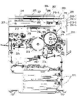
Fig. 2 is an outside view of an apparatus
according to the first embodiment of the present
invention.
12
x.2112737
In Fig. 2, the apparatus comprises an image
scanner unit 201 and a printer unit 200. The image
scanner unit 201 is for picking up an original image
and digitizes it into an electrical signal. The
printer unit 200 is for printing on a paper a full-
color image corresponding to the original image picked
up by the image scanner unit 201.
The image scanner unit 201 comprises a
pressing plate 202. An original 204 carried on an
original carrier glass plate (hereinafter, referred to
as a platen) 203 is illuminated with light produced by
a halogen lamp 205. The halogen lamp 205, which
serves as a light source, produces light beams
involving wavelengths corresponding to the infrared
region. The light reflected from the surface of the
original is guided to mirrors 206 and 207 and is
focused by a lens. 208 on a four-line sensor
(hereinafter, referred to as a CCD) 210. The CCD 210
separates colors of the optical information obtained
from the original. The separated colors are supplied
to a signal processing unit 209 as full-color
information consisting of red (R), green (G) and blue
(B) components and an infrared (IR) component. The
entire area of the original is scanned by mechanical
movement of the lamp 205 and the mirror 206 at a
velocity v, and of the mirrors 207 at a velocity v/2,
r
13
2~1~~3~
in a direction perpendicular (hereinafter, referred to
as a sub scan direction) to the electrical scanning
direction (hereinafter, referred to as a main scan
direction) of the four-line sensor 210.
A standard white plate 211 generates a
correction data for correcting shading of read data
210-1 through 210-4 (correction of characteristics of
an individual element of each line sensor)
corresponding to the line sensors IR, R, G and B,
respectively. The standard white plate 211 reflects
light that is relatively balanced in all visible and
infrared wavelengths. In other words, the standard
white plate 211 reflects light at substantially
uniform reflectance, as shown in Fig. 7, and appears
white to the eyes. This standard white plate 211 is
adapted to generate data used for shading correction
on the output data of the IR sensor 210-1 and of the
visible sensor 210-2 through 210-4.
The signal processing unit 209 electrically
processes the signals obtained by the scanning
operation to separate it into components of magenta
(M), cyan (C), yellow (Y) and black (BK), which are
sent to the printer unit 200. Either one of the
components M, C, Y, and BK is supplied to the printer
unit 200 at every one scanning operation of the image
scanner unit 201, so that a complete color image
14
corresponding to one original is obtained through
four-time scanning operation.
The image signals representing the respective
components M, C, Y and BK supplied from the image
scanner unit 201 are sent to a laser driver 212. The
laser driver 212 drives a semiconductor laser 213 in
response to the image signal supplied from the image
scanner unit 201. The semiconductor laser 213 emits a
laser beam and the emitted beam scans a photosensitive
drum 217 through a polygon mirror 214, an f-8 lens
215, and a mirror 216.
A developing unit is composed of a magenta
developing station 219, a cyan developing station 220,
a yellow developing station 221 and a black developing
station 222. These four developing stations are
successively brought into contact with the
photosensitive drum 217, thereby developing
electrostatic latent images of M, C, Y and BK formed
on the photosensitive drum 217 with toners
corresponding to the respective colors.
A sheet fed from a sheet cassette 224 or 225
is wound on a transfer drum 223, and receives the
transfer of the image developed on the photosensitive
drum 217.
15
After completion of transferring each of four
color images of M, C, Y and BK, the sheet is
discharged through a fixing unit 226.
The halogen lamp 205 is commonly used for
visible and infrared information readings. It
produces light composed of a band of frequencies
required for these readings. Such common source of
light contributes to effective illumination of light
with different wavelengths to the original which are
required for visible and infrared information
readings.
Figs. 6A and 6B illustrate the CCD 210 applied
to the present embodiment.
The infrared sensor 210-1 is a photosensitive
element line (CCD line sensor) used for sensing
infrared radiation. The photosensitive element lines
210-2, 210-3, and 210-4 are for sensing R, G, and B
waveform components (visible spectra), respectively.
Each of the IR, R, G and B sensors 210-1 through 210-4
has openings of 10 um in width and in length along the
main and sub scan directions, respectively. These
photosensitive element lines are different in optical
characteristics from each other and are arranged
monolithically on a single silicon chip such that the
IR, R, G and B sensors are arranged in parallel to
each other to sense the same line on the original.
16 ~~ 7
The above mentioned structure of the CCD
allows common usage of optical system such as a lens
for visible and infrared readings.
This makes it possible to improve the accuracy
of optical adjustment or the like and facilitate the
adjustment as well.
A reference numeral 210-5 represents a glass
plate of approximately 300 um in thick. The hatched
portion of the glass is treated to have an infrared
cutoff characteristic. For this purpose, the glass
plate 210-5 is provided with a dichroic mirror 210-11
formed of a deposition film. The characteristic of
this infrared cutoff region is shown in Fig. 10. In
this event, the glass plate 210-5 is adhered to the
surface of the chip with the deposited region facing
to the sensors.
Referring to Fig. 9, described is a filter
spectral characteristic of each of the line sensors
IR, R, G and B in the CCD 210.
The sensor 210-2 is provided with a filter
210-8 having a characteristic indicated by R in Fig. 9
that has sensitivity to light of red and infrared
spectra. Likewise, the sensor 210-3 is provided with
a filter 210-9 having a characteristic indicated by G
in Fig. 9 that has sensitivity to light of green and
infrared spectra. The sensor 210-4 is provided with a
CA 02112737 2001-06-11
17
filter 210-10 having a characteristic indicated by B
in Fig. 9 that has sensitivity to light of blue and
infrared spectra. The IR sensor 210-1 is sensitive
only to the infrared radiation corresponding to the
region represented by cross-hatched portion in Fig. 9.
As apparent from the figure, the filters 210-8
through 210-10 are sensitive to the infrared radiation
having a wavelength o~f '700 nm or more. With this
respect, the infrared. cutoff filter 210-11 used is so
selected that it has the characteristic illustrated in
Fig. 10.
Fig. 6B is an enlarged illustration of the
photosensitive elements. Each sensor is 10 um in
length for every one pixel along the main scan
direction. Five thousand sensors are aligned along
the main scan direction for each CCD line sensor to
read the width (297 mm) of an A3-paper at a resolution
of 400 dpi. In addition, the R, G and B line sensors
are away from each other at a distance of 80 um, which
corresponds to an eight-line distance relative to a
sub scan resolution of 400 l.pi (line per inch). The
IR sensor 210-1 is away from the R sensor 210-2 at a
distance of 160 Nm (16 lines), a double of other line
distance.
Fig. 8 shows spectral response of an
infrared absorber marketed under the trade-mark
SIR-159 (sold by Mit;~ui Toatsu Chemicals
18
__ ~ 2~ 1273
Inc., Chiyoda-ku, Tokyo, Japan) used in this
embodiment as a detected mark on a specific original.
In this embodiment, the IR sensor 210-1 is directed to
sense the infrared with wavelength ranging between 750
and 850 nm to detect presence of this infrared
absorber.
To this end, the lens 208 is provided with a
far infrared cutoff filter formed of a dichroic mirror
having spectral response as illustrated in Fig. 11.
This filter is harmless for the R, G and B sensors
210-2 through 210-4 as well as for the IR sensor 210-
1, so that it is provided with a common lens unit, the
lens 208. This allows a design for the filter
provided for the lens 208 to be determined only by the
consideration of the far infrared cutoff
characteristic. As a result, superior far infrared
cutoff characteristic can be achieved with a simple
interference fringe structure.
Fig. 14 is a block diagram for use in
describing flow of the image signals in the image
scanner unit 201. Each of the image signals is
supplied from the CCD 210 to an analog signal
processing unit.3001. The analog signal processing
unit 3001 changes the magnitude of the image signal
with a gain constant. The offset is also adjusted in
the analog signal processing unit 3001. The image
19
signals for the respective colors (including IR) are
then supplied from the analog signal processing unit
3001 to respective A/D converters 3002 through 3005.
Each of the A/D converters 3002 through 3005 converts
the analog image signal into a digital image signal of
8 bits. The digital image signal is supplied to
corresponding one of shading correction units 3006
through 3009 where it is subjected to known shading
correction using a reading signal obtained for the
standard white plate 211.
A clock generator 3019 generates a clock
signal at a speed corresponding to data of one pixel
carried by the digital image signal. The clock signal
is supplied to a line counter (a main scan address
counter) 3020 that counts the number of clock signals
to produce a pixel address output for one line. A
decoder 3021 decodes a main scan address supplied from
the main scan address counter 3020 to generate a CCD
driving signal, a VE signal and a line synchronization
signal HSYNC. The CCD driving signal may be shift
pulses or reset pulses for every one line while the VE
signal indicates a valid section in a one line reading
signal supplied from the CCD.
As shown in Figs. 6A and 6B, the line sensors
210-1, 210-2, 210-3 and 210-4 in the CCD 210 are
spaced from each other at a predetermined distance.
20
Line delay elements 3010, 3011 and 3012 are provided
for correcting the spatial displacement. More
specifically, the image signals obtained from the IR,
R and G sensors 210-1, 210-2 and 210-3 proceed the
image signal out of the B sensor 210-4 in the sub scan
direction. With this respect, the line delay elements
3010, 3011 and 3012 line-delay the IR, R and G signal
in the sub scan direction relative to the B signal.
Light-to-density conversion (logarithmic)
units 3013, 3014, 3015 are composed of look-up table
ROMs and convert luminance signals of R, G and B into
density signals of C, M and Y. A known masking and
undercolor removal (UCR) circuit 3016 generates, from
input signals Y, M and C representing three primary
colors, output signals of Y, M, C, and Bk with a
predetermined number of bits (f or example, 8 bits), at
each scanning operation carried out by the image
scanner unit 201.
A discrimination unit 3 detects a specific
pattern on the original, which is a feature of the
present invention. A CPU 3018 carries out sequence
control involving, for example, control to the
original reading optical systems and ON/OFF control of
the original illumination lamp 205. The CPU 3018
produces a pixel section signal VSYNC in the sub scan
direction. The CPU 3018 also serves to control a
21
zl~z~.~~
selector 3017 in response to a result of judgment
supplied from the discrimination unit 3 such that a
port output rather than the reading signal is supplied
to the printer, thereby effectively prohibiting
copying operation for a specific original.
Fig. 15 is a timing chart for each control
signal.
The VSYNC signal indicates the image valid
section in the sub scan direction and assumes a level
"1" in the entries for scanning the image to
successively produce the output signals of (M), (C),
(Y) and (Bk). VE is a signal indicating the image
valid section in the main scan direction and takes, in
the section of level "1", timing at the start position
of the main scanning operation. A CLOCK signal is a
pixel synchronization signal which causes the transfer
of the image data at the leading edge from "0" to "1".
Next, an image pattern to be detected in the
present invention is described referring to Fig. 3.
Fig. 3 is a view illustrating an example of a
pattern formed with a transparent ink containing a
-glazing dye having the spectral response as shown in
Fig. 8. A triangular pattern a is printed with an ink
excluding the infrared with a certain range of
wavelength. A small square pattern b having sides of
120 um in length is overlapped with the triangle and
22 ~,1~~'13?
printed thereon with the above mentioned transparent
ink.
This pattern appears substantially same to the
human eye, as shown in Fig. 8, in the visible
spectrum. However, it can be detected in the infrared
region by means of determining the infrared absorption
characteristics of the pattern. While the square
pattern having the sides of approximately 120 um is
illustrated here for the later description, the region
corresponding to this pattern b requires four pixels
as shown in the figure when being read at 400 lpi
(line per inch). It is noted that a method of forming
the pattern in not limited to that described here.
Details of the discrimination unit is
described with reference to Fig. 4 in which 10-1
through 10-4 represent image data line delay units.
Each of the image data line delay units 10-1 through
10-4 is composed of a first-in-first-out (FIFO)
memory. An address pointer thereof is initialized
with a line synchronization signal HSYNC, which is not
shown in this figure. The CLOCK signal is used for
writing data into the FIFO memory for every one pixel
and reading the same out of the memory. The image
data line delay units 10-1 through 10-4 delay a 32-bit
data (eight for each IR, R, G and B) by one line.
23
~11~~~~
More specifically, the input signal is delayed
and latched by 2 pixels at flip-flops 11-1 and 11-2 to
produce a pixel data A. The line memories 10-1 and
10-2 delay this signal by two lines to produce a pixel
data C. This pixel data C is delayed by four pixels
to produce a notable pixel data X and a pixel data B.
All of these signals A, C and X are supplied to a
judgment unit 12. Likewise, a pixel data D is
produced and supplied to the judgment unit 12.
Fig. 5 shows the positional relation between
the notable pixel data X and other four pixels A, B, C
and D therearound. As apparent from the figure, when
the notable pixel X corresponds to the pattern b (Fig.
3), then the pixels A, B, C and D all correspond to
the peripheral area, the image of the pattern a.
Fig. 12 is a view showing geometry of visible
and infrared radiation reflected from various
originals and corresponding states of infrared reading
signals. In Fig. 12, (a-1) is a cross-section of the
specific original identification pattern shown in Fig.
3. An infrared absorbing ink 2802 is on the face of a
paper 2801. The incident light from the halogen lamp
205 is reflected from the infrared absorption pattern
and its peripheral portion. In this figure, R1, G1,
B1, IRIl, R1', G1', B1', IRI1', R2, G2, B2, IRI2, R2',
G2', B2', IRI2', R3, G3, B3, IRI3, R3', G3', B3' and
24
IRI3' are values obtained by means of sensing the
reflected light by the R, G, B and IR sensors and
converting these analog signal to the digital ones,
following which the shading correction and line delay
processings are made.
These read values are given, for the R, G and
B visible information, as the spectral characteristics
corresponding to a combination of characteristics of
the R, G and B sensors in Fig. 9 and the infrared
cutoff filter in Fig. 10.
In this event, R represents the light with
wavelengths primarily in the 590 to 620 nm range, G
represents the light with wavelengths primarily in the
500 to 580 nm range and B represents the light with
wavelengths primarily in the 400 to 480 nm range.
The infrared information, IR, is given as the
spectral characteristic obtained by combining or
multiplying the characteristics of R, B (the cross-
hatched range in Fig. 9) and the far infrared cutoff
characteristics shown in Fig. 11. More specifically,
IR represents the light with wavelengths primarily in
the 710 to 850 nm.
The light in each of the wavelength ranges R,
G, B and IR is corrected independently, during the
shading correction, in sensitivity by using the
standard white plate having a uniform reflectance to
25
2 ~ 12?'~'~
each wavelength in Fig. 7. In this embodiment, the
light is corrected in sensitivity such that the R, G,
B and IR reading values are equal to each other to the
original having a relatively uniform spectral
characteristic as the standard white plate as shown in
Fig. 7.
In Fig. 12, (a-2) is a graphical
representation of the reading signal values obtained
for the infrared absorption pattern and the peripheral
portion thereof after the shading correction of the R,
G, B and IR.
The specific pattern in this embodiment has
substantially same color in the visible region as
shown (a) in Fig. 13 and the signal values of the
visible R, G, and B become equal accordingly.
The concentration of the infrared absorbing
substances contained in the infrared absorbing ink is
so adjusted that the infrared reading signal IR 2
obtained from the infrared absorption pattern is
smaller than the minimum values of the visible
information R2, G2 and B2 for the same infrared
absorption pattern. The visible color of the specific
original identification pattern consists of colors
which are relatively high in saturation. This means
that the minimum values of the visible color
26
211 ~ '~ ~ 7
separation signals R, G and B for the identification
pattern become relatively small.
When the infrared absorbing ink does not
satisfy the above mentioned conditions, the gain
constant used for the shading correction on the above
mentioned IR reading signal may be decreased, ensuring
that the IR2 signal obtained from the infrared
identification pattern to be detected is smaller than
the minimum values of R2, G2 and B2.
Described now is a case where the original is
read under this reading conditions. An original (b-1)
in Fig. 12 has a back on which a carbon black (having
the infrared absorption characteristics) 2803 is
printed.
The visible reading signals for this original
are similar to those obtained in (a-1). The infrared
radiation is absorbed by the carbon black 2803 and, as
a result, the infrared read value IR3 becomes smaller
than the read value IR1 obtained from around the
carbon black. Thus, the reading signal (b-2) exhibits
similar characteristics to the reading signal (a-2)
obtained from the infrared absorption pattern b.
In this embodiment, the IR reading signal IR1
obtained from the infrared absorbing ink is smaller
than any one of the visible reading signals R1, G1 and
B1. On the contrary, the infrared back-through
27
component IR2 obtained from the typical carbon black
is not smaller than the minimum values of the visible
read values R3, G3 and B3 in most cases. This is
because the identification pattern a has the visible
colors of high saturation and the minimum values of
R2, G2 and B2 are relatively small while the infrared
back-through component is not sufficiently absorbed by
the carbon black on the back of the original and thus
the infrared information has a relatively large value.
By detecting this characteristic, it becomes
possible in this embodiment to discriminate the
identification pattern printed with the infrared
absorbing ink from the back through due to the carbon
black.
Described in conjunction with (c-1) and (c-2)
in Fig. 12 is a case where the infrared back-through
component IR3' is smaller than any one of the visible
back-through components R3', G3' and B3'. This
corresponds to a case where the carbon black is soaked
into the original or where the original itself is a
thin paper. The visible colors are different from the
peripheral portions, according to which it is possible
to discriminate the back-through from the
identification mark in the form of the infrared
absorption pattern in (a-1). This is because the
identification pattern a has, as mentioned above, the
28
2~ ~.2~~'l
visible colors of high saturation; the minimum values
of R2, G2 and B2 are relatively small; the
identification pattern is so determined that the IR2
is read with its value being smaller than any one of
the minimum values of R2, G2 and B2; and the
sensitivity is set relative to the color separation
reading for R, G, B and IR, so that if the infrared
back-through component is smaller than the visible
components or R3', G3' and B3' as in (c-1) and (c-2),
the back-through also affects on the visible signals.
The R, G, B and IR reading signals obtained
from a dirt identification pattern is shown in (d-1)
and (d-2) in Fig. 12. A banknote on which a specific
pattern is printed is contaminated during circulation
in the market for a long time. Such contamination or
dirt affects on each of the R, G, B and IR signals as
a uniform attenuation factor. Consequently, the
infrared reading signal IR2' for the infrared
absorbing pattern is smaller in value than the visible
information R2', G2' and B2' even when the original is
dirt.
Fig. 13 shows the relation between the reading
signals of the visible and infrared information for
each of the above mentioned case.
29 I~ 2 ~ ~ 2
Now, described below is a judgment algorithm
carried out by the judgment unit 12 of this
embodiment.
Let the R, G, B and IR components of the
reading signal composing the pixel signal A be AR, A~,
AB and AIR, respectively, then average values YR, Yc.
YB and YIR of the reading signals of the corresponding
color components R, G, B and IR in each of the pixel
signals B, C and D are given as follows:
1 O YR = 1 / 4 ( AR + BR + CR + DR ) ,
YG = 1 / 4 ( A~ + B~ + C~ + D~ ) ,
YH = 1/4(A$ + BH + CH + DH), and
Y=R = I / 4 ( AIR + B=R + CIR + DIR )
Judgment of the target pattern is made according to
the difference between the notable pixel X and the
average value Y obtained from the above equation.
More specifically, let the R, G, B and IR
components of X be XR, XG, XB and XIR, then
aR = I YR _ XR I ,
2 0 ~G = I Y~ - Xc ( ~
nB = IYB - xHI, and
SIR = YIR - XIR.
In this event, the original is judged as the specific
pattern when the following equations are satisfied:
DR < K
and DG < K
21 1 2737
and OB < K
and D ( SIR > Ll or YIg~XIR > L2 and XIR < min ( XR,
Xc~ Xs)~
where K, L1 and L2 are constants.
More specifically, the pattern is judged to be
present when the difference in color is small (smaller
than K) between the notable pixel X and any one of the
peripheral portions A, B, C and D in the visible
region; when the difference is equal to or larger than
the constant L1 in the infrared region; when the ratio
of the level of the notable pixel X to that of the
periphery is equal to or larger than the constant L2
in the infrared region; and when the signal value of
the infrared notable pixel X is smaller than the
visible color separation signal of the same notable
pixel.
In this event, the ratio is taken into
consideration along with the difference in judging the
infrared region in view of the reduction of the signal
level of the infrared signal due to dirt on the
original. In this embodiment, any affects of the dirt
is eliminated by means of detecting the ratio,
provided that the infrared reading signal is entirely
attenuated due to the dirt.
31 ~ 2 1 9 2737.
Fig. 1 shows the structure of the judgment
unit 12 for use in realizing the above mentioned
algorithm.
An adder 121 merely adds the color components
of four pixels and produces the eight high-order bits
of the sum to obtain YR, Yc, YH and YIR. A subtractor
122 calculates a difference between the output of the
adder 121 and corresponding component of the notable
pixel signal to obtain DR, DG and AB components. The
subtractor 122 supplies five high-order bits of the
subtraction results to a judgment LUT 128 consisting
of ROMs. The LUT 128 produces "1" when each of the
~R, DG and ~B components is smaller than a constant K
(in this embodiment, the constant K is set at eight
levels). Likewise, for the infrared reading signal,
YIR and XIR of eight bits each are supplied to address
terminals of a judgment LUT 129 consisting of ROMs.
The LUT 129 produces "1" when the above mentioned
judgment result holds, that is, AIR > L1 or YIR~XIR >
L2 holds as well as SIR - YIR - XIR.
Simultaneously, a min extraction unit 131
extracts the minimum value min (R, G, B) of the R, G,
and B color separation signals XR, X~ and XH,
respectively for the notable pixel. A comparator 132
compares the min (R, G, B) with the infrared reading
signal for the notable pixel. The comparator 132
32 ~. 2 1 1 2 7 3 7
produces "1" when YIR < min (R, G, B) holds. The
outputs of the LUTs and the comparator are supplied to
an AND gate 130 to obtain a logical product thereof.
The AND gate 130 produces an output signal MK. The
output signal MK indicating "1" corresponds to the
condition where presence of the specific pattern is
detected.
The judgment result is supplied to a latch 3022
in Figs. 14A and 14B. An output of the latch 3022 is
supplied to an input port P10 of the CPU 3018. The
CPU 3018 confirms that the specific mark is detected.
The CPU 3018 clears the latch 3022 by an output port
P9 signal before initiation of a copy sequence. The
CPU 3018 is thus ready for the subsequent pattern
detection.
Referring to Fig. 16, description will be made
in conjunction with a normal copying operation and an
identification mark judging operation accompanying
thereto carried out under control by the CPU 3018.
When an operator put the original 204 on the
platen 203 and initiates the copying operation through
an operation unit (not shown), the CPU 3018 controls a
motor (not shown) to move the reflection mirror 206
beneath the standard white plate 211. The halogen
lamp 205 is turned on to illuminate the standard white
plate 211. The shading correction units 3006 through
33 . 2 1 1 2 7 3 7
3009 sample the shading data for the IR, R, G and B
signals (Step 1).
Subsequently, the port output P is set into
"0" to clear the output of the latch 3022 into "0"
and, in turn, clear the P8 output into "0". The input
A of the selector 3017 is selected such that the image
signals masked and subjected to the undercolor removal
(UCR) are supplied to the printer. The output P9 is
set to "1" to stop the clear operation of the latch
3022 (Step 2).
Next, the scanning operation is repeated four
times as the printer unit 200 records four colors of
M, C, Y and BK to complete one copy of the original.
At the same time, presence of the identification mark
is detected and the recording operation is controlled
in accordance with the detection result.
The CPU 3018 sets, for recording magenta,
processing conditions for magenta into the masking UCR
processing unit 3016. Subsequently, the CPU operates
the optical system to supply a signal indicating
magenta to the printer 200. After completion of the
scanning operation, the optical system is turned back
to an initial position of scanning (Step 3).
The CPU periodically reads the input signal
supplied to the port 10 during the scanning operation
to determine whether the input signal indicates "1".
34 _ z ~ ~ z ~ 3
If the P10 is "1", outputs of PO through P7 are set
into FFH at step 7 based on the decision that the
predetermined original is to be copied. In addition,
an output of P8 is set into "1" to supply the printer
200 a set-solid signal of FFH, whereby prohibiting
further copying operation to avoid counterfeit of the
specific original.
Likewise, the recording control is also made
for cyan, yellow and black through steps 4 to 6,
during which the CPU periodically checks the P10. If
the P10 is "1" the CPU supplies the set-solid FFH data
to the printer 200 at step 7.
For example, when P10 = 1 is detected during
cyan recording, only magenta is recorded through a
normal or proper copying operation. The remainders,
cyan, yellow and black are recorded as solid of FFH.
A way for prohibiting a normal copying
operation may be, other than a set-solid, a batching
processing, interruption of image forming means,
turning off the power or the like.
<Second Embodiment>
Typical infrared absorbing inks are slightly
colored in the visible region and sufficient level of
the infrared absorbing characteristic may be achieved
causing a difference in color between the infrared
absorbing and non absorbing portions in the visible
35 _ 2 1 1 2 7 3 7
region. With such the infrared absorbing ink, it is
difficult to lower the signal level of the infrared
reading signal than the color separation signal in the
visible region, though it is achieved in the first
embodiment. This embodiment is directed to avoid
incorrect or erroneous identification of the back-
through on a normal original by means of using the
visible information to a mark printed with the ink of
the type described.
The infrared absorbing mark to be detected in
the second embodiment is so formed that the infrared
reading signal value is lower than the luminosity
level obtained by the values of the visible color
separation signals of R, G and B.
In addition, as in the first embodiment, the
infrared reading signal is compared with luminosity
signals generated from the visible color separation
signals, thereby determining whether the read pixel is
associated with a predetermined mark.
Now, described below is a judgment algorithm
carried out by the judgment unit 12 of this
embodiment.
In this embodiment, a luminosity signal L is
obtained from the visible color separation signals of
R, G and B according to the following equation:
L = (R + 2G + B)/4.
2 1 9 2 7 37
36
Let the R, G, B and IR components of the
reading signal composing the pixel signal A be AR, A~,
AB and AIR, respectively, then average values YR, Yc.
YB and YIR of the reading signals of the corresponding
color components R, G, B and IR in each of the pixel
signals B, C and D are given as follows:
YR - 1 / 4 ( AR + BR + CR + DR ) .
Y~ = Z/4(A~ + BG + C~ + D~).
Y$ = 1 /4 ( A$ + BH + C$ + DB ) , and
IO YIR = 1/4 (AIR + BIR + CIR + DIR)
Judgment of the target pattern is made according to
the difference between the notable pixel X and the
average value Y obtained from the above equation.
More specifically, let the R, G, B and IR
components of X be XR, X~, X$ and XIR, then
DR = ~YR - XR~,
OG = ~ Y~ - X~ ~ ,
AB = I Y$ - XH I ,
SIR = Y=R - XIR , and
XL = ( XR + 2X~ + XB) /4 .
In this event, the original is judged as the specific
pattern when the following equations are satisfied:
DR < K
and DG < K
and ~B < K
and ~(DIR > L1 or YIR/XIR > L2 and XIR < XL,
where K, L1 and L2 are constants.
37
. 2112737
More specifically, the pattern is judged to be
present when the difference in color is small (smaller
than K) between the notable pixel X and any one of the
peripheral portions A, B, C and D in the visible
region; when the difference is equal to or larger than
the constant L1 in the infrared region; when the ratio
of the level of the notable pixel X to that of the
periphery is equal to or larger than the constant L2
in the infrared region; and when the signal value of
the infrared notable pixel X is smaller than the
visible color separation signal of the same notable
pixel.
Fig. 17 shows the structure of the judgment
unit 12 for use in realizing the above mentioned
algorithm.
The adder 121 merely adds the color components
of four pixels and produces the eight high-order bits
of the sum to obtain YR, Y~, Y$ and YIR. The
subtractor 122 calculates a difference between the
output of the adder 121 and corresponding component of
the notable pixel signal to obtain DR, DG and OB
components. The subtractor 122 supplies five high-
order bits of the subtraction results to the judgment
LUT 128 consisting of ROMs. The LUT 128 produces "1"
when each of the DR, DG and OB components is smaller
than a constant K (in this embodiment, the constant K
38
~ Z11273~-
is set at eight levels). Likewise, for the infrared
reading signal, YIR and XIR of eight bits each are
supplied to address terminals of the judgment LUT 129
consisting of ROMs. The LUT 129 produces "1" when the
above mentioned judgment result holds, that is, SIR >
L1 or YIR~Xig > L2 holds as well as DIR - YIR - XIR.
Simultaneously, an AND calculation unit 131
extracts a luminosity signal KL of the R, G, and B
color separation signals XR, X~ and XH, respectively
for the notable pixel. The comparator 132 compares
the luminosity signal KL with the infrared reading
signal for the notable pixel. The comparator 132
produces "1" when YIR < KL holds. The outputs of the
LUTs and the comparator are supplied to the AND gate
130 to obtain a logical product thereof. The AND gate
130 produces an output signal MK. The output signal
MK indicating "1" corresponds to the condition where
presence of the specific pattern is detected.
The result of judgment is processed by the CPU
3018 in the same manner as in the first embodiment.
The similar processing to that in the first embodiment
is performed for detection a specific original and
avoiding counterfeit of it.
<Third Embodiment>
In this embodiment, to further improve the
accuracy of detection on the specific mark, the signal
4 2~ X273).
level of the infrared reading signal at the infrared
reflecting portion around the infrared absorbing ink
portion of the mark is higher than the maximum value
of the visible color separation signals.
More particularly, possibility of the
incorrect judgment of the back-through on the normal
original is reduced by means of setting the infrared
reading signal value at the infrared absorption
portion is smaller than the minimum values of the
visible color separation values. In addition, the
infrared reading signal value at the infrared
reflecting portion is larger than the maximum values
of the visible color separation values. As a result,
a feature less found in a normal original can be
provided.
In addition, as in the first embodiment, the
infrared reading signal is compared with luminosity
signals generated from the visible color separation
signals, thereby determining whether the read pixel is
associated with a predetermined mark.
Now, described below is a judgment algorithm
carried out by the judgment unit 12 of this
embodiment.
40 ; ~ 1 1 2737_
w
Let the R, G, B and IR components of the
reading signal composing the pixel signal A be AR, AG,
A$ and AIR, respectively, then average values YR, YG.
Y$ and YIR of the reading signals of the corresponding
color components R, G, B and IR in each of the pixel
signals B, C and D are given as follows:
YR = 1/4(AR + BR + CR + DR),
YG = 1 / 4 ( AG + BG + CG + DG ) .
Y$ = 1/4 (A$ + BH + CH + D$ ) , and
IO YIR = 1/4 (AIR + BIR + CIR + DIR)
Judgment of the target pattern is made according to
the difference between the notable pixel X and the
average value Y obtained from the above equation.
More specifically, let the R, G, B and IR
components of X be XR, XG, XB and XIR, then
DR = ~ YR - XR ~ ,
DG = I YG - XG I ,
AB = ~YB - XBI,
DIR = Y=R - XIR . and
XL = ( XR + 2X~ + XB) /4 .
In this event, the original is judged as the specific
pattern when the following equations are satisfied:
DR < K
and DG < K
and OB < K
and ~(DIR > L1 or YIR/XIR > L2
41 r 21 1273?
and XIR c min (XR, Xc, XB)
and YIR > max ( YR, Yc, Y$ ) .
where K, L1 and L2 are constants.
More specifically, the pattern is judged to be
present when the difference in color is small (smaller
than K) between the notable pixel X and any one of the
peripheral portions A, B, C and D in the visible
region; when the difference is equal to or larger than
the constant L1 in the infrared region; when the ratio
of the level of the notable pixel X to that of the
periphery is equal to or larger than the constant L2
in the infrared region; when the signal value of the
infrared notable pixel X is smaller than the visible
color separation signal of the same notable pixel; and
when the average value of the infrared signal values
of the peripheral pixels is larger than the maximum
value of the average values of the visible color
separation signals.
Fig. 18 shows the structure of the judgment
unit 12 for use in realizing the above mentioned
algorithm.
The adder 121 merely adds the color components
of four pixels and produces the eight high-order bits
of the sum to obtain YR, Yc, YH and YIR. The
subtractor 122 calculates a difference between the
output of the adder 121 and corresponding component of
4 2 _. 2 1 1 2 7 3 l~
the notable pixel signal to obtain DIt, DG and AB
components. The subtractor 122 supplies five high-
order bits of the subtraction results to the judgment
LUT 128 consisting of ROMs. The LUT 128 produces "1"
when each of the DR, DG and ~B components is smaller
than a constant K (in this embodiment, the constant K
is set at eight levels). Likewise, for the infrared
reading signal, YIR and XIR of eight bits each are
supplied to address terminals of the judgment LUT 129
consisting of ROMs. The LUT 129 produces "1" when the
above mentioned judgment result holds, that is, DIR >
L1 or YIR~XIR > L2 holds as well as DIR - YIR - XTR
Simultaneously, the min extraction unit 131
extracts the minimum value min (R, G, B) of the R, G,
and B color separation signals XR, XG and XH,
respectively for the notable pixel. The comparator
132 compares the min (R, G, B) with the infrared
reading signal for the notable pixel. The comparator
132 produces "1" when YIR < min (R, G, B) holds. The
outputs of the LUTs and the comparator are supplied to
an AND gate 130 to obtain a logical product thereof.
The AND gate 130 produces an output signal MK. The
output signal MK indicating "1" corresponds to the
condition where presence of the specific pattern is
detected.
43 _,
Simultaneously, a Max extraction unit 134
extracts the maximum value max (R, G, B) of the R, G,
and B color separation signals YR, Y~ and YH,
respectively for the notable pixel. A comparator 135
compares the max (R, G, B) with the average value of
the infrared reading signals for the peripheral pixel.
The comparator 135 produces "1" when YIR > max (R, G,
B) holds. The outputs of the LUTs and the comparator
are supplied to the AND gate 130 to obtain a logical
product thereof. The AND gate 130 produces an output
signal MK. The output signal MK indicating "1"
corresponds to the condition where presence of the
specific pattern is detected.
The result of judgment is processed by the CPU
3018 in the same manner as in the first embodiment.
The similar processing to that in the first embodiment
is performed for detection a specific original and
avoiding counterfeit of it.
<Modifications>
While the above embodiments 1 through 3 have
thus been described in conjunction with detection of a
specific mark, the present invention is also
applicable to detection of a mark having an infrared
reflecting characteristic provided on a base having an
infrared absorbing characteristic.
44
In addition, the present invention is not
21 1 2737-
limited to discrimination of a particular infrared
mark. It can also be applied to detect a mark having
an absorbing or reflecting characteristic to the
ultraviolet radiation.
Further, a mark having a fluorescent
characteristic to other wavelength regions other than
the visible region may also used instead of using the
one having the absorbing or reflecting characteristic.
In such a case, the invisible reading signal may be
compared with the visible reading signal.
As mentioned above, according to the
embodiments 1 through 3 of the present invention, it
is possible to detect the mark in a higher accuracy by
means of comparing, upon detecting a specific mark
using invisible information, the signal level of the
reading signal thereof with the signal level of the
visible reading signal. In addition, is possible to
reduce significantly the incorrect or erroneous
judgment to the normal original.
<Fourth Embodiment>
It is known that typical printing inks are
reflective to the light of the infrared region.
However, some color materials exhibit significant
absorbing characteristic in the infrared region though
appeared transparent in the visible region. An
45
example of such color material is SIR-159 available
from Mitsui Toatsu Chemicals Inc., of which spectrum
response is shown in Fig. 19. It is a challenge to
use such a color material for the security purpose
that is transparent in the visible region while is
absorbent or reflective in the infrared region. The
visible effect of it depends on refraction of light,
back reflection and the cfllor reflected light
radiation from the substance.
More particularly, in a pattern shown in Fig.
20, areas A and B appear same color (visible) in the
visible region while invisible pattern recognition can
be made when infrared absorbance is detected in the
area B. For example, the area A may be a ground color
(nothing is printed thereon) of the valuable
securities of the like and the area B may be printed
with the transparent ink having the spectrum response
shown in Fig. 19, thereby allowing the areas A and B
to be used as a common pattern for all valuable
securities.
However, considering by the wavelength
characteristic shown in Fig. 19, it is impossible to
extract or detect a particular one waveform to
discriminate it from the infrared absorption of the
specific pattern. This is because some color
materials such as carbon black commonly used are
46 i 2 1 1 2 7 3 7.
absorbent to the light with relatively wide range
including the wavelengths absorbed by the above
mentioned transparent ink. As a result, determination
of the absorbing characteristic on a single wavelength
is not sufficient for positively discriminate the
transparent ink from the carbon black.
With respect to this, the present invention
overcomes the above mentioned problem by the
following.
The fourth embodiment of the present invention
is now described with reference to a block diagram
shown in Fig. 21. Fig. 21 is a structural block
diagram of a color copying machine. An image reading
sensor 2001 consists of sensor cells provided with red
(R), green (G) and blue (B) color separation filters,
respectively, and a sensor cell provided with an
infrared filter. The color separation filters are for
reading the corresponding visible information from the
original while the infrared filter is for reading the
specific pattern as infrared information. The output
of the IR cell is supplied to a judgment unit 2005, a
feature of the present invention, to determine whether
the original is the valuable securities. On the other
hand, RGB visible image information is converted into
a record signal by a general color image processing
unit 2002. The record signal is composed of cyan (C),
t,219273~J
magenta (M), yellow (Y) and black (BL) and is supplied
to a record control unit 2003. The record control
unit 2003 controls the image processing when the
judgment unit 2005 judges that the original is the
specific one such as the valuable securities. In this
event, the record control unit 2003 controls the image
processing by means of, for example, pasting black ink
on the entire area under processing or ceasing the
recording operation.
The image reading sensor 2001 is composed of
two cell groups as shown in Fig. 22. A line 2010 is
formed of filters of R, G and B alternatively arranged
with each other to produce serial visible information.
On the other hand, a line 2011 produces an
infrared component obtained by means of dividing a
single pixel into two different wavelength components
IR1 and IR2. More specifically, the IR1 component is
centered on ~,1 = 800 nm at which the absorbing
characteristic of the ink arrives peak while the IR2
component is centered on ~2 = 900 nm at which the
reflecting characteristic is exhibited again.
One of the features of the present invention
is to detect the infrared characteristic according to
at least two wavelength components to specify the
infrared characteristic of the ink to be
discriminated.
_ 21 1273,
",
To determine the infrared absorption only on
the basis of IR1 does not make it possible to
discriminate the infrared ink from the carbon black or
the like. In this event, detection of the infrared
reflection at IR2 assures the presence of the
transparent ink for avoiding counterfeit.
In other words, the original is judged as the
specific one, the valuable securities in this
embodiment, when
IR1 < K1 and IR2 > K2
i
is satisfied.
In this event, the ration or IRZ/IR1 is used
as a criteria for judgment in view of the entire
reduction of the reflectance due to dirt or the like.
Fig. 23 shows an exemplified structure of the
judgment unit 2005 applied to the present invention.
A comparator 2050 compares a predetermined constant K1
with an output IR1 of the IR sensor at the wavelength
of 800 nm. The comparator 2050 supplies "1" to an AND
circuit 2053 when the reflected light is smaller in
amount than the constant K1, i.e., when the ink
absorbs the light. A divider 2051 calculates a ratio
of IR2/IR1. A comparator 2052 compares the ratio with
a constant KZ (K2 > 1) and supplies "1" to the AND
circuit 2053 when the ratio is equal to or larger than
K2.
49 _ 2 1 9 2 7 3 7
The output of the AND circuit is the final
result of judgment and the logical value "1" of the
output indicates that the ink characteristic shown in
Fig. 19 is detected.
<Fifth Embodiment>
To further positively detect the infrared
characteristic of the ink, an spectral output IR3 may
be obtained at, for example, 7~3 = 1000 nm. In this
event, the specific pattern of the transparent ink is
judged to be present when a condition (K3 > 1 K3 >
K2 ) in
IRl < Kl and IRZ > K2 and IR3 > K3
i i
is satisfied.
<Sixth Embodiment>
In this embodiment, ~4 = 700, ~.1 = 800 and a.2
900 are defined to detect the specific pattern in a
higher accuracy. Besides, each output value is
subjected to so-called masking processing with the
respective values to correct profiles of filters for
detecting IR4, IR1 and IR2.
~ IR'4 = a11IR4 + a12IR1 + a13IR2i
~ IR' 1 = a21IR4 + a22IR1 + a2glRa, and
~ IR' Z = a31IR4 + ag2IR1 + ag3IR2 r
where all through a33 are coefficients.
In addition, IR'4 and IR'Z are normalized with IR'1,
then
50 ~. 2~'2~3a.
rv ~ 2~
IR4 ..~ IR
IR4 = IRl, IRZ = IR1~~
N N
when li < IR4 < 12 and 13 < IR2 < 14
it is judged that the specific pattern is present.
Fig. 24 shows an exemplified structure for use
in carrying out the above mentioned judgment
algorithm. A masking circuit 2054 composed of a
multiplier and an adder supplies the sensor
output divided through the filters into three spectra
with central wavelengths of 700 nm, 800 nm and 900 nm,
respectively. The masking circuit 2054 carries out
the above mentioned correction calculation using data
supplied from a coefficient memory 2055.
IR'4 and IR'Z are normalized with IR'1 by
dividers 2056 and 2057, respectively, to provide an
output given by the following equation:
IR4 and IR2,
which are supplied to a judgment ROM 2058. The ROM
2058 is so-called LUT (look-up table) where judgment
results are written previously according to 11 through
14 in the above equation.
By normalizing with IR'1, it becomes possible
to determine the infrared absorbing characteristic
without being affected by dirt or contamination.
<Modification>
51
' ~ ~ ~ , 3~
While this embodiment has thus been described
in conjunction with judgment as one point for every
one pixel, the input infrared image data may be
calculated as an average of a plurality of pixel
values. Alternatively, the final judgment may be made
in response to completion of accumulation of a
predetermined number of the judgment results.
According to the above mentioned embodiments 3
through 6,
(1) it is possible to judge the original without
requiring any focus relative to the infrared region
because the judgment is not based on a pattern
matching;
(2) a cost saving apparatus can be achieved with less
cycle of calculation;
(3) the sensor cells are not necessarily assigned to
the same pixel at IR, IR2 and IR3 because no pattern
matching is used. Consequently, it is not required to
correct shift or displacement of reading position of
the sensor, allowing cost saving design of the
apparatus. In addition, it is not necessary to
consider a relation between the pattern size and the
resolution of the sensors) used.
<Seventh Embodiment>
Fig. 25 shows the reflectance of the ink with
being printed on a paper that is to be detected in
52 - 2 1 ~ 2 7 3
this embodiment. The ink appears transparent in the
visible region while has the infrared absorbing
characteristic in the infrared region. For example,
the characteristic curve A is for the ink
representative of SIR-159 (sold by Mitsui Toatsu
Chemicals Inc.) which exhibits sufficient absorbing
characteristic at and around 800 nm. An ink B of the
similar kind is less absorbent to the infrared
radiation, so that the ink A can be discriminated from
the ink B by means of detecting the reflected light at
and around 800 nm.
Fig. 26 illustrates an example where the inks
A and B are printed concentrically on a paper. It
will be invisible at all when being printed at about 1
mm in diameter on a portion of a common valuable
securities where no other print is made. It is noted
that typical papers reflect the light with this
wavelength entirety (about 100%), so that the
difference in the reflectance between the inks A and B
can readily be detected.
In Fig. 26, (a-1), (b-1) and (c-1) show
examples where the infrared absorbing inks A and B are
concentrically printed on the paper of ground color
having a 100% reflectance. The patterns are read as
the change of one-dimensional reflectance of being
illustrated in (a-2), (b-2) and (c-2), respectively,
53 . 2 1 1 2 7 37_
when the scan line, passing through the center of the
pattern as depicted by an arrow, is read.
The apparatus according to this embodiment is
similar in structure to those illustrated in Fig. 21,
so that further detailed description will be omitted.
An embodiment of the judgment unit 2005 is
described using (b-1) in Fig. 26 as an example. In
Fig. 27, a sensor signal is quantized and coded into
an 8-bit infrared reading signal. This reading signal
is supplied to comparators 3051 and 3052 where it is
digitized with constants K1 and K2 (K2 < K1) as
thresholds, that is:
when IR > K1, the read portion corresponds to
the ground color,
when K2 ~ IR a K1, the read portion
corresponds to the ink B, and
when IR < K2, the read portion corresponds to
the ink A.
When the output of the comparator 3051 is "0",
the read portion corresponds to the ground color.
When the output of the comparator 3051 is "1" while
that of the comparator 3052 is "0", the read portion
corresponds to the ink B. When the outputs of the
comparators 3051 and 3052 are "1", the read portion
corresponds to the ink A. The output signals of the
comparators are delayed by one pixel by flip-flops
54
t 2112737
(FFs) 3053-1 through 3053-7 and FFs 3054-1 through
3054-6 to detect the pattern b shown in Fig. 26 in a
one-dimensional manner from the reflected light. More
particularly, the read portion is judged as the ink A
when an AND gate 3055 detects that the outputs of the
FFs 3053-1 and 3054-1 are both "1" and an output
terminal thereof is supplied with a signal of logic
"1". Likewise, when the output of the F/F 3053-2 is
"1" and that of the F/F 3054-2 is "0", an AND gate
3056 produces an output of logic "1" and the read
portion is judged as the ink B. It is found that the
ground color is present in two adjacent pixels when
the outputs of the F/F 3053-3 and 4 are "0".
Accordingly, when the output of an gate
circuit 3060 is "1", detected is the infrared pattern
of "ground color", "ink A," "ink B", "ground color",
"ground color", "ink B", "ink A" and "ground color".
While the output of the infrared sensor is
judged with the fixed threshold values, it is apparent
that the output is corrected (shading correction)
before judgment by using the light illuminating the
standard plate at every time when the image is scanned
as in the case of typical copying machines.
While this embodiment has thus been described
on the assumption that the transparent ink used is
ref lective at approximately 100 in the visible
21 12737s
region, a similar pattern and detection thereof may be
provided with a plurality of inks that appear same
color to the human eye and that have different
reflecting characteristics to the light with a
5 specific wavelength in the infrared region.
In addition, while this embodiment has thus
been described in conjunction with a pattern printed
with two divergent inks A and B, the possibility of
erroneous judgment can be reduced without complicating
10 the pattern by means of using three or more inks
together.
The pattern is not limited to the concentric
shape and any one of adequate shapes can be selected
that is suitable for the pattern matching.
15 Depending on the pattern, a two-dimensional
pattern matching technique can be used.
<Modif ication>
While the above embodiment has thus been
described in conjunction that the recording signal is
20 controlled to control the recording after detection of
the specific pattern, an image scanner or the like for
supplying images into a computer or the like is
applicable to control in various ways. For example,
the scanner may be used for controlling the reading
25 signal, interrupting the reading or deleting the
signal already picked up.
56 ' 2 1 1 2 7 3 7_
As mentioned above, there is an effect that
the possibility of the incorrect judgment can be
reduced for normal originals by means of reading at a
plurality of levels the pattern formed of a plurality
of inks having different reflectance to the light with
the infrared wavelength, thereby specifying the
pattern according to the level and the shape.
<Eighth Embodiment>
(Characteristics of an Original)
This embodiment makes it possible to
discriminate images of higher accuracy by using, as a
specific image, color materials formed of a color
having substantially no absorbance to the infrared
radiation in which infrared absorbing substances are
contained.
Fig. 28 shows the spectral reflective
characteristic of the color material used in the
present invention.
This color material is highly reflective to
the light with the wavelength of from 600 nm to 700
nm. It absorbs the light with the wavelength of from
700 nm to 900 nm.
To provide such characteristic, incorporated
in a typical red material is a substance (in this
embodiment, SIR-175 available from Mitsui Toatsu
Chemicals Inc.) that appears transparent in the
21 12737._
57 .--_
visible region while absorbs the light in the near-
infrared region.
The present inventor had studied and
investigated spectral reflective characteristics of
about 1000 different print inks at the wavelengths of
300 nm to 1100 nm.
In particular, the inventor had focused on the
near-infrared region of between 700 nm and 900 nm. As
a result, it has revealed that the absorption of the
light with the near-infrared wavelengths shows the
following tendencies.
1. Some color materials of high thickness and low
saturation have absorption to the light with the near-
infrared wavelengths.
2. Some greenish materials having high saturation
have absorption to the light with the near-infrared
wavelengths.
In addition, the color materials had also
studied on reflection to the infrared radiation. As a
result, it has revealed that there is no reddish
material absorptive to the infrared.
Accordingly, it is understood that to use a
color material having the infrared absorbing
characteristic which appears red or reddish in the
visible region is a safety method to discriminate a
specific original.
21 12731_
58
An example of an original that should not be
copied is shown in Fig. 35. Illustrated is a copy
prohibited original (hereinafter, merely referred to
as an original) 4630 on which a pattern 4631 is
printed with a paint that appears red and has the
infrared absorbing characteristic.
The original 4630 contains, other than the
pattern 4631, secret information and an image 4632
printed thereon with a common ink.
Fig. 30 is an outside view of an apparatus
according to this embodiment of the present invention.
In Fig. 30, the apparatus comprises an image
scanner unit 4201 and a printer unit 4202. The image
scanner unit 4201 is for picking up an original image
and digitizes it into an electrical signal. The
printer unit 4202 is for printing on a paper a full-
color image corresponding to the original image picked
up by the image scanner unit 4201.
The image scanner unit 4201 comprises a
mirror-faced pressing plate 4200. An original 4204
carried on an original carrier glass plate
(hereinafter, referred to as a platen) 4203 is
illuminated with light produced by a halogen lamp
4205. The light reflected from the surface of the
original is focused by a lens 4209 on a color sensor
(hereinafter, referred to as a CCD) 4210. The CCD
59 t: 2 1 1 2 7 37
4210 separates colors of the optical information
obtained from the original. The separated colors are
supplied to a signal processing unit 4211 as full-
color information consisting of red (R), green (G) and
blue (B) components and an infrared (IR) component.
The entire area of the original is scanned by
mechanical movement of a reading unit 4207 at a
velocity v in a direction perpendicular (hereinafter,
referred to as a sub scan direction) to the electrical
scanning direction (hereinafter, referred to as a main
scan direction) of the color sensor.
The signal processing unit 4211 electrically
processes the signals obtained by the scanning
operation to separate it into components of magenta
(M), cyan (C), yellow (Y) and black (BK), which are
sent to the printer unit 4202.
(Structure of the Printer Unit)
The image signals representing the respective
components M, C, Y and BK supplied from the image
scanner unit 4201 are sent to a laser driver 4212.
The laser driver 4212 drives a semiconductor laser
4213 in response to the image signal supplied from the
image scanner unit 4201. The semiconductor laser 4213
emits a laser beam and the emitted beam scans a
photosensitive drum 4217 through a polygon mirror
4214, an f-8 lens 4215, and a mirror 4216.
_..
~2~37
A developing unit 4218 is composed of a
magenta developing station 4219, a cyan developing
station 4220, a yellow developing station 4221 and a
black developing station 4222. These four developing
stations are successively brought into contact with
the photosensitive drum 4217, thereby developing
electrostatic latent images of M, C, Y and BK formed
on the photosensitive drum 4217 with toners
corresponding to the respective colors.
A sheet fed from a sheet cassette 4224 or
4225 is wound on a transfer drum 4223, and receives
the transfer of the image developed on the
photosensitive drum 4217.
After completion of transferring each of four
color images of M, C, Y and BK, the sheet is
discharged through a fixing unit 4226.
That's all for the description of the scanner
and printer units, the major components of the
apparatus.
Next, the image scanner unit 420T is described
more in detail.
Figs. 29A and 29B show structures of the CCD 4210.
Figs: 29A and 29B show a top plan view and a
sectional view, respectively, of the CCD 4210.
The CCD 4210 is formed of a first pixel train
4100 and a second pixel train 4101. The first pixel
.,
r~~ ~r' ~
61 ~_ 2 1 1 2731
train comprises filters alternatively arranged with
each other to produce serial visible information.
More specifically, R filters 4102, G filters 4103 and
B filters 4104 are deposited alternatively in order of
R, G, B, R, G, B ...to form a minimum reading system
with one pixel 4105 or a set of three pixels R, G and
B being used as a minimum reading area.
Fig. 31 shows the spectral characteristic of
the filters deposited for each pixel while Fig. 32
shows the emission spectral characteristic of the
halogen lamp 4205.
The second pixel train 4101 comprises pixels
aligned at a pitch three times larger than that in the
first pixel train 4100. More particularly, the second
pixel pitch is equal to the pixel pitch in the first
pixel train 4100. The second pixel train 4101 is
provided with a visible light cutoff filter deposited
thereon that has the characteristic shown in Fig. 33.
Accordingly, the light with the wavelengths not longer
than 700 nm is cutoff by the pixel train 4101 and only
the infrared components can be read.
As apparent from Fig. 29B, the second pixel
train 4101 is shifted by 300 um as a step d to
elongate the optical path therefor. This is because
the focal distance of the optical system depends on
the wavelength and the infrared radiation required
62 ' 2 1 1 2 l 37
longer optical path, otherwise the image will be out
of focus .
Fig. 34 shows dimensions of the first and the
second pixel trains 4100 and 4101 as well as the
positional relation therebetween. In this event, the
reading unit is assumed to have the resolution of 400
dpi. In addition, for the purpose of clarifying the
description, the optical system used is assumed to be
a one-power optical system.
To realize the resolution of 400 dpi, the
minimum reading area is 63.5 Nm x 63.5 um in
dimension. Thus, each of the R pixel 4102, the G
pixel 4103 and the B pixel 4104 in Fig. 34 is 21.1 pm
x 63.5 pm in dimension while the IR pixel is 63.5 um x
63.5 ~m in dimension. The distance between the pixel
trains 4100 and 4101 is set to 127 ~Cm in this
embodiment. In other words, the pixel trains are away
from each other by an amount equal to two pixel
trains. The reading signals obtained by the pixel
trains 4100 and 4101 are supplied to the signal
processing unit 4211.
Next, a sequence of the pattern recognition is
described in order.
In this embodiment, description is made in
conjunction with a copy prohibited original (such as a
secret document) as an example of an original directed
63 ,_ y 2 1 1 2 7 3 7
to counterfeit prohibition. However, the present
invention is not limited to those particularly
described and illustrated embodiment, and is also
applicable to bills, notes, valuable securities or the
like.
(Pre-scanning)
The image scanner unit 4201 performs a pre-
scanning operation as a pre-processing for copying an
original 4630. This Pre-scanning is described.
First, the lamp 4205 illuminates a white
shading plate 4640 attached to a portion of the platen
4203. An reflected image from the white shading plate
4640 is focused on the CCD 4210 through the lens 4209.
The image from the white shading plate 4640 is read by
the pixel trains 4100 and 4101 in the CCD 4210. The
read image is subjected to signal processing in the
signal processing unit 4211 to create correction data
for correcting uneven illumination of the lamp 4205 as
well as non-uniformly sensitivity of the pixel trains
4100 and 4101 in the CCD 4210. The correction data is
stored for every pixel train.
Next, the reading unit 4207 moves mechanically
through a driving system (not shown) at a velocity v
in a direction depicted by an arrow m, thereby
scanning the entire surface of the original. In this
event, the image on the original 4630, read by the
64 t 2 1 1 2 7 ~~:
pixel train 4100 in the CCD 4210, is sampled on the
minimum and maximum values of the depth of the
original. A print depth set value for a copy is then
calculated according to the sampled values.
Subsequently, the reading unit 4207 moves mechanically
to an initial position or a home position through a
driving system (not shown) at the velocity v in a
direction depicted by an arrow n in Fig. 36.
(Copy of original and Pattern Sensing)
After completion of the above mentioned
shading correction data creation, the reading unit
4207 turns back to the home position to initiate
reading of the original 4630. Simultaneously, the
reading unit 4207 detects whether the pattern 4631 is
present on the original 4630.
The presence and absence of the pattern is
determined according to the reading information
obtained by the pixel train 4100 in the CCD 4210 and
to a comparison result obtained by comparing the
reading information. Pixel reading for reproducing
the image is performed by the pixel train 4100 while
image reading for detecting the pattern 4631 is
performed by the pixel train 4101.
Described below is the signal processing unit
4211 for processing the read signal.
65
Fig. 37 shows a block diagram of the signal
processing unit 4211.
First, a signal processing system of the pixel
train 4100 is described. Analog image signals are
supplied from the pixel train 4100 in order of R, G
and B in synchronism with the driving signal for CCD
4210. The image signals are supplied simultaneously
to three sample and hold circuits 4121a through 4121c.
The sample and hold circuit 4121a generates a
sampling signal at a same timing as the R signal is
received. The sample and hold circuit 4121a holds the
analog level of the sampled signal until the
subsequent R signal is received. Likewise, the sample
and hold circuit 4121b generates a sampling signal at
a same timing as the G signal is received while the
sample and hold circuit 4121c generates a sampling
signal at a same timing as the B signal is received.
As a result, the sample and hold circuits
4121a, 4121b and 4121c produce R, G and B signals,
respectively. These signals are, as shown in the
figure, supplied to the respective A/D converters
4122a through 4122c where the analog image signals are
converted into digital image signals, each having
eight bits. These digital signals are supplied to the
respective shading correction circuits 4124a through
4124c where they are subjected to shading correction.
66 I_ 2 1 1 2 7 37
The shading correction is correction
processing described in the above mentioned "Pre-
scanning" section. The generated correction data are
held in an RAM 4123 for each of the R, G and B data.
In reading the image, the correction data,
each of which corresponding to one pixel, are
successively supplied to the shading correction
circuits 4124a through 4124c to correct the data. The
image signals supplied from the shading correction
circuits 4124a through 4124c are sent to a five-by-
five edge emphasis circuit 4125. The five-by-five
edge emphasis circuit (hereinafter, merely referred to
as the edge emphasis circuit) 4125 is a circuit for
emphasizing the outline or configuration of the read
image and is realized by the following.
Fig. 38 shows a structure of the edge emphasis
circuit 4125. The edge emphasis circuit 4125 is
provided for each color though only one of them is
illustrated in Fig. 38. It is noted the edge emphasis
circuit for the remaining two colors are equal in
structure and operation to the one illustrated in the
figure.
In Fig. 38, reference numerals 4131 through
4134 are FIFOs capable of holding data for one line of
the pixel train 4100 in the CCD 4210. Connection
among four FIFOs are as shown in the figure. When a
6' . , 2 1 1 2 7 3 7,
pixel train data regarding to the n-th line is
supplied to the FIFO 4131, the FIFOs 4131, 4132, 4133
and 4134 produce data regarding to the (n-1)-th, (n-
2)-th, (n-3)-th and (n-4)-th lines, respectively. An
input signal and the outputs signal supplied from the
FIFOs 4131 through 4134 are sent to a delay circuit
4135. The delay circuit 4135 comprises pixel delay
circuits of a few stages for the m-th pixel signal
received. The delay circuit 4135 supplies the m-th,
(m-1)-th, (m-2)-th, (m-3)-th and (m-4)-th pixel data
to an arithmetic circuit 4136. Thus, the arithmetic
circuit 4136 is supplied with the data for twenty-five
pixels in total.
A map of the data supplied is shown in Fig.
39.
The data of twenty-four peripheral pixels are
supplied to the arithmetic circuit 4136 relative to
the cross-hatched notable pixel. The arithmetic
circuit 4136 multiplies the notable pixel by twenty-
five to obtain data of 25-fold of the notable pixel,
from which the data about the twenty-four peripheral
pixels is subtracted. When the data of the notable
pixel is larger than that of the peripheral pixels,
then the notable data becomes larger. Likewise, when
the data of the notable pixel is smaller than that of
68 _C11Z73~~
the peripheral pixels, then the notable data becomes
smaller.
Such processing makes a sharp contrast along
the configuration of the image, emphasizing the
contrast of the reproduced image. The image data
subjected to the edge emphasizing is supplied to the
printer unit through a logarithmic conversion unit
4127 and a masking conversion unit 4128. The
logarithmic conversion unit 4127 is for light-to-
density conversion while the masking conversion unit
4128 is for the optimum correlated color correction.
That's all for the description of signal
processing unit of the pixel train 4100.
Next, a signal processing system of the pixel
train 4101 is described. This signal processing
system is essentially similar to those of the pixel
train 4100 except that it has no edge emphasis circuit
because reproduction of the image is not a goal of
this system.
The data supplied from a shading correction
circuit 4124b is sent to a signal comparison circuit
4126. Other inputs of the signal comparison circuit
4126 are connected to the edge emphasis circuit 4125.
It is noted that, as apparent from Fig. 39, the
notable pixel in the edge emphasis circuit 4125
corresponds to the data of the (n-2)-th line. To
69 . 2 1 1 1 7 37
compare the data of the pixel train 4100 with that of
the pixel train 4101, a line buffer is required to
compensate distance between them by two lines as shown
in Fig. 34. However, the edge emphasis is made on the
pixel train 4100, so that the reading data for the
same portion on the original are provided.
The signal comparison circuit 4126 compares
the pixel data of the pixel train 4100 with that of
the pixel train 4101 to supply the comparison result
to the CPU (which is not shown in this figure).
In comparing the signals, calculated is a sum
of the number of the pixels satisfying:
IR - R < kl,
R > G, and
R > B,
where kl is a constant.
When the calculation result exceeds the predetermined
number of the pixels, the CPU controls to interrupt
immediately copying of the original.
<Ninth Embodiment>
According to this embodiment, the wavelengths
to be read by the pixel train 4101 is 700 nm or
longer. However, as shown in Fig. 28, the spectral
distribution of an infrared absorbing painting
exhibits gradually increased reflectance at or longer
than 900 nm. Depending on the light source used, the
~o
.21'2737.
spectral energy may spread to the region with the
wavelengths of 1000 nm or longer. To use the light
source of the type described makes it difficult to
determine absorption due to the unnecessary energy at
the region with the wavelengths of 900 nm or longer.
With this respect, the pixel train 4101 is preferable
to have a far-infrared cutoff filter that has the
characteristic as shown in Fig. 40.
For the pixel train 4100, the far-infrared
cutoff filter may be arranged at any adequate location
within the optical path because the far-infrared
radiation has already cut off by the filters deposited
on the surface of the pixels. For example, the far-
infrared cutoff filter may be advantageously arranged
in front of and back of the lens 4209. With such
arrangement, the filter can be replaced or changed
readily when the fluorescent characteristic of a
fluorescent paint printed later on the original.
<Tenth Embodiment>
While the this embodiment has thus been
described in conjunction that the line positions of
the pixel trains 4100 and 4101 are corrected by using
the FIFO applied to the five-by-five edge emphasis
circuit, this embodiment is applies alternative
design. For example, the FIFO may be replaced with an
image processing circuit implementing an FIFO for
71
21 1 2~3~~
error diffusion processing or so on. The FIFO may be
provided only for the line position correction.
<Eleventh Embodiment>
According to this embodiment, judgment of the
pattern is made only by means of signal comparison by
the signal comparison circuit. However, the pattern
matching may be made on the basis of a shape of the
image extracted as a result of signal comparison,
thereby to control copying of the original. In such a
case, a pattern matching circuit becomes large and
complex but it is possible to determine type of the
original according to the shape of it. Accordingly,
alternative or selectable control can be provided
allowing to copy, for example, a company document
using a pass-word while prohibiting to copy the
valuable securities or the like.
A solid image pick-up device may be, other
than the above mentioned charged coupled device (CCD),
MOS or amplifying device where a capacity load
(electrode) is connected to the emitter of a photo-
transistor as disclosed in U. S. Patent No. 4,791,469
to Tadahiro OHMI and Nobuyoshi TANAKA.
As mentioned above, it is possible to detect
formed patterns in a high accuracy by means of forming
on the copy prohibited original a predetermined
pattern with the color material obtained by applying
~___ 2 1 1 2 7 37;
the infrared absorbing characteristic to color having
no infrared absorbing characteristic, thereby reading
the original by the device comprising infrared
radiation reading means in the copying machine.
<Twelfth Embodiment>
In Japanese Patent Application No. 5-15095,
assigned to the same applicant as the present
invention, a device is suggested that refers a
specific mark and the ground portion therearound to
discriminate the specific mark under the condition
where the mark and the ground are substantially same
in color to each other while are significantly
different from each other about the signal values
regarding to the infrared information reading.
In addition, Japanese Patent Application No.
5-6978, assigned to the same applicant as the present
invention, discloses formation of a mark of which
relative configuration with respect to a certain
reference point.is not changed when the original on
which the mark is printed is rotated. For example,
the mark may be circular in shape that is not affected
by the mounting angle of the original relative to the
glass carrying it thereon.
A specific mark and the ground are printed
with different inks when the mark is printed on the
face of a paper under the condition where the mark and
_2~ ~27~x~
the ground are substantially same in color to each
other while are significantly different from each
other about the signal values regarding to the
infrared information reading. In other words, the
mark and the ground are printed on the paper with an
ink A transmitting the infrared radiation and an ink B
absorbance to the infrared radiation, respectively,
both of which appear specific color.
The inks A and B should appear same color in
the visible region.
The carbon black is generally known as a
material having the infrared absorbing characteristic.
In addition, some greenish material also have the
infrared absorbing characteristic. These materials
appear black or green in the visible spectrum.
Accordingly, it is difficult to make the color of the
inks A and B same in spite of much effort to obtain,
with the infrared absorbing materials, the ink B that
is substantially equal in color to the ink A having
arbitrary color of the ground.
In addition, SIR-159 available from Mitsui
Toatsu Chemicals Inc. or the like is known as the
infrared absorbing material that appears color closer
to transparent in the visible spectrum. However, it
has a color close to gray and thus it is difficult to
prepare the inks A and B appearing the same color.
.2112737
With this respect, the inks A and B for the
ground portion and the mark portion, respectively, may
be detected in the visible region as the same color
though their colors are slightly different from each
other. This technique requires the apparatus to
detect different colors as the same one and, in turn,
increases the possibility of incorrect judgment of
information in a general printed matter as the
specific mark.
Further, to print a mark of which relative
configuration with respect to a certain reference
point is not changed when the original on which the
mark is printed is rotated results in enlargement of
the mark itself. As a result, printing method for the
original such as the banknotes should be changed,
notifying the presence of the mark of common people.
This affects on the secrecy of the original.
This embodiment is directed to detect, with
respect to the above problem, a specific mark upon
reading thereof by means of obtaining contrasts
between the visible reading signals and between the
invisible reading signals upon to discriminate the
specific mart according to the correlation between the
visible and invisible contrasts.
In addition, this embodiment is directed to
determine whether the original is the specific one by
~5 , ~ ~ ~ 2 7 ~~
means of detecting a mark printed on the original with
the infrared absorbing ink in the form of a donut as a
completely symmetric mark.
This embodiment is now described in detail.
An apparatus according to this embodiment is similar
in structure to those described in conjunction with
Fig. 2, thus further description thereof will be
omitted.
The image scanner 201 is described in detail.
The halogen lamp 205, which serves as the
light source, is commonly used for visible and
infrared information readings. It produces light
composed of a band of frequencies required for these
readings. Such common source of light contributes to
effective illumination of light with different
wavelengths to the original which are required for
visible and infrared information readings.
Figs. 51A and 51B illustrate the CCD 210
applied to the present embodiment.
The infrared sensor 210-1 is the
photosensitive element line (CCD line sensor) used for
sensing infrared radiation. The photosensitive
element lines 210-2, 210-3, and 210-4 are for sensing
the R, G, and B waveform components (visible spectra),
respectively. Each of the IR, R, G and B sensors 210-
1 through 210-4 has openings of 10 um in width and in
76
y '? 7 1 2 7 3 ~~
length along the main and sub scan directions,
respectively. These photosensitive element lines are
different in optical characteristics from each other
and are arranged monolithically on a single silicon
chip such that the IR, R, G and B sensors are arranged
in parallel to each other to sense the same line on
the original.
The above mentioned structure of the CCD
allows common usage of the optical system such as a
lens for visible and infrared readings.
This makes it possible to improve the accuracy
of optical adjustment or the like and facilitate the
adjustment as well.
A sectional view taken on the dotted line in
Fig. 51A is shown in Fig. 51B.
Mounted on a silicon substrate 210-5 are a
photo sensor 210-1 for IR reading and photo sensors
210-2, 210-3 and 210-4 for reading visible information
of R, G and B, respectively. The R-photo sensor 210-2
is provided with an R-filter 210-7 adapted to transmit
red component of the visible light. Likewise, the
sensor 210-3 is provided with a G-filter 210-8 and the
sensor 210-4 is provided with a B-filter 210-9.
Referring to Fig. 9, described is a filter
spectral characteristic of each of the line sensors
IR, R, G and B in the CCD 210.
77 2112737
The characteristic indicated by R is an output
characteristic of a sensor obtained by the R-filter
210-7 having sensitivity to light of red and infrared
spectra. Likewise, characteristic indicated by G is
an output characteristic of a sensor obtained by the
G-filter 210-8 having sensitivity to light of green
and infrared spectra. The characteristic indicated by
B is an output characteristic of a sensor obtained by
the B-filter 210-9 having sensitivity to light of blue
and infrared spectra. The IR sensor 210-1 is provided
with the red filter 210-7 and the blue filter 210-9
with being overlapped to each other and is thus
sensitive only to the infrared radiation corresponding
to the region represented by cross-hatched portion in
Fig. 9.
As apparent from the figure, the R, G and B
filters 210-7 through 210-9 are sensitive to the
infrared radiation having a wavelength of 700 nm or
more. With this respect, the infrared cutoff filter
210-11 is provided for the R, G and B photo sensors.
This infrared cutoff filter 210-11 is formed of
laminated deposition films of Si02 and Ti02 and has
the characteristic illustrated in Fig. 10. A
reference numeral 210-6 represents an equalized layer
formed of transparent organic films.
21 1 273,
Fig. 8 shows spectral response of an infrared
absorber SIR-159 (sold by Mitsui Toatsu Chemicals
Inc., Chiyoda-ku, Tokyo, Japan) used in this
embodiment as a infrared absorbing material for a
detected mark on a specific original. In this
embodiment, the IR sensor 210-1 is directed to sense
the infrared with wavelength ranging between 750 and
850 nm to detect presence of this infrared absorber.
To this end, the lens 208 is provided with a far
infrared cutoff filter 231 formed of a dichroic mirror
having spectral response as illustrated in Fig. 52a.
As a result, the spectral sensitivity of the
IR sensor 210-1 is given as the spectral
characteristic obtained by combining or multiplying
the characteristics of the cross-hatched range in Fig.
9 and the characteristic shown in a in Fig. 52. As
apparent from this characteristic shown in b in Fig. 52,
IR represents the light with infrared wavelengths
primarily in the 710 to 850 nm.
This filter 231 is harmless for the R, G and B
sensors 210-2 through 210-4 as well as for the IR
sensor 210-1, so that it is provided with a common
lens unit, the lens 208. This allows a design for the
filter provided for the lens 209 to be determined only
by the consideration of the far infrared cutoff
characteristic. As a result, superior far infrared
7 9 ~, _ -- ~ ~ 2 1 1 2 7 3 ~,~
cutoff characteristic can be achieved with a simple
interference fringe structure.
Fig. 51B is an enlarged illustration of the
photosensitive elements. Each sensor is 10 um in
length for every one pixel along the main scan
direction. Five thousand sensors are aligned along
the main scan direction for each CCD line sensor to
read the width (297 mm) of an A3-paper at a resolution
of 400 dpi. In addition, the R, G and B line sensors
are away from each other at a distance of 80 um, which
corresponds to an eight-line distance relative to a
sub scan resolution of 400 lpi (line per inch). The
IR sensor 210-1 is away from the R sensor 210-2 at a
distance of 160 Nm (16 lines), a double of other line
distance.
A block diagram for use in describing flow of
the image signals in the image scanner unit 201 is
similar to that illustrated in Figs. 14A and 14B.
Referring now to Fig. 42, described is an
image pattern to be detected in the present invention.
A donut-shaped pattern shown in Fig. 42 is a specific
mark to be detected in this embodiment. The ink B,
having the infrared absorbing characteristic as shown
in Fig. 8, is printed in the donut shape on the ground
of the ink A absorbing no infrared radiation. This
ink B having the infrared absorbing characteristic is
8° ~_Z11Z7~7
prepared by incorporating infrared absorbing materials
into the ink A transmitting the infrared radiation.
As the infrared absorbing material, the color material
SIR-159 are used that appears substantially
transparent in the visible region and has a
characteristic of absorbing the light in the infrared
region. The SIR-159 has a color closer to gray in the
visible region, so that mere incorporation of the SIR-
159 into the ink A results in the ink B darker than
the ink A. With this respect, the ink B is prepared
by incorporating the infrared absorbing material, SIR-
159, into an ink having higher saturation than the ink
A: As a result, the inks A and B are substantially
same in color in the visible region. The pattern b is
thus indistinguishable by the human eye, but is
clearly discriminated in the infrared region.
As shown in Fig. 42, the linear width of the
donut portion printed with the ink B is 250 um, which
corresponds to about four pixels when being read at
the resolution of 400 dpi.
Since the ink A differs from the ink B,
displacement of registration is caused upon being
printed. The amount of displacement may sometimes
correspond to the amount of one pixel at the
resolution of 400 dpi.
81 ~ _ 2 1 9 2 7 3 ?~
Fig. 43 shows the printed result with a
displacement corresponding to the amount of one pixel.
As apparent from the figure, the linear width of the
donut portion printed with the ink B corresponds to
the amount of three pixel while the center portion of
the donut printed with the ink A also corresponds to
the amount of three pixel. In addition, a phase shift
between the digitizing phase upon reading and the
phase of the original is basically equal in amount to
one pixel. With the displacement upon printing and
the phase shift upon reading between the CCD and the
mark taken into consideration, a valid reading section
of 2 pixels is ensured in the mark having four-pixel
linear width.
In this embodiment, a noise component upon
reading is eliminated by means of taking an average of
the adjacent two pixels and then the mark is detected.
In this manner, to use the mark having the minimum
area of four-pixel size allows reading of the mark
less affected by the registration and the noise.
An advantage of forming the donut portion
using the infrared absorbing ink B is described below.
The same circular marks can be formed into a circular
pattern.
The donut-shaped pattern is the simplest one
of the circular patterns. When the infrared absorbing
8 2 .~ ._. _ 2 ~ ~ 2 7 3 7
ink B is printed on the central portion of the
circular mark as shown in (1) in Fig. 44, the central
portion is surrounded by the ink A, a common printing
ink. This is a mere isolated dot as it is. Such dot-
s like circle cannot be discriminated from a dirty spot
or dot information in the halftone dot printing and
thus is not suitable for the specific mark. An effort
to form the specific mark with a multiple circle
rather than the donut in (1) in Fig. 44 will results
in a triple circular mark as shown in (2) in Fig. 44
because the ground itself is the ink A. Such pattern
is not practical because it requires enlarged judgment
circuit and a large area for printing the pattern.
With this respect, the present embodiment applies the
double circle formed of the infrared absorbing ink B
printed around the common ink reflective to the
infrared radiation. As a result, it becomes possible
to form a specific mark, that is less possible to be
contained in the printing, in a minimum printing area
and to make the mark not to be recognized by the human
eye. In addition, the scale of the judgment circuit
can be reduced into minimum.
It is noted that the pattern is not limited to
those described and illustrated above, it may be a
predetermined pattern arranged along the periphery of
83
21 1 273?.
a circle (Fig. 44; (3)) or may be a pattern of which
ring is different in thickness (Fig. 44; (4)).
<Outline of Mark Detection>
As mentioned above, this embodiment detects
the specific mark formed as a donut with the infrared
absorbing ink B and the infrared reflecting ink A,
both of which appear substantially same color in the
visible region. There are two major methods for
detecting the pattern:
1. a difference between visible color signals is
small and a difference between infrared signals is
large; and
2. a pattern has a donut-shape.
Described with reference to Figs. 45A and 45B
is an outline of detection of the difference between
the visible color signals and the difference between
the infrared signals.
Fig. 45A shows a donut mark printed with the
infrared absorbing ink (Security Ink) B indicated by
an area B on the ground of the infrared transmitting
ink A indicated by an area A. The color separation
signals for the R, G and B visible lights, obtained
from the area A, are represented by Ra, Ga and Ba,
respectively, and an infrared light-amount signal is
represented by IRa. Likewise, the color separation
signals for the R, G and B visible lights, obtained
84 ~. 2 1 1 ~ 7 3l_
from the area B, are represented by Rb, Gb and Bb,
respectively, and an infrared light-amount signal is
represented by IRb. It is assumed that the infrared
absorbing ink B is prepared by blending the infrared
absorbing material with the infrared transmitting ink
A. As shown in Fig. 45B, with the infrared absorbance
of the mixed infrared absorbing material being
defined, then a difference SIR between the infrared
signal values of IRa and IRb is given as follows:
SIR = IRa x (Absorbance).
According to this equation, the infrared absorbance of
the incorporated infrared absorbing material can be
given by:
(Absorbance) _ ~IR/IRa.
The DIR/IRa is generally called a contrast of the IR
signal. More particularly, the infrared absorbance
not depending on the absolute values of IRa and IRb
can be obtained by means of calculating the contrast
IR.
In the same manner, to obtain a difference
among visible colors, this embodiment calculates a
contrast R, a contrast G and a contrast B according to
the following equation. Absolute values are used for
calculating the R, G and B contrasts because which
reading values for the ink A and the ink B is not
necessarily determined.
85
'. 21 12737_
Contrast R = ~Ra - Rbl / Ra = AR/Ra,
Contrast G = ~Ga - Gb~ / Ga = OG/Ga,
Contrast B = ~Ba - Bbd / Ba = ~B/Ba, and
Contrast IR = (IRa - IRb) / IRa = ~IR/IRa.
It is determined whether the above mentioned "1. a
difference between visible color signals is small and
a difference between infrared signals is large" is
satisfied.
In Fig. 46, an abscissa represents the
contrast of the visible color separation signals while
an ordinate represents the contrast of the infrared
signal.
In Figs. 45A and 45B, smaller difference
between the visible color signals in the areas A and B
indicates that the contrast of the visible color
separation signals is small. On the contrary, larger
difference between the visible color signals in the
areas A and B indicates that the contrast of the
visible color separation signals is large. In this
way, the specific mark according to this embodiment
can be plotted on the area close to the ordinate.
In Fig. 46, a straight line CB inclined at an
angle of 45° relative to the horizon is the
characteristic curve of the carbon black when it is
used as the infrared absorbing material. When the ink
B is prepared by incorporating the carbon black into
86
f_ 21 12737
the ink A, the contrasts between the ink A and the ink
B are approximately similar in the visible and
infrared regions because the carbon black has a
uniform light absorbing characteristic to the light
with the wavelengths in the range of from the
ultraviolet to the infrared. This means that, in
considering an effect of the carbon black that is
widely used in printed matters, the cross-hatched area
corresponds to the characteristic expected to be
obtained in a general printed matter. The cross-
hatched area extends above the CB line because of the
back-through characteristic of a general printed
matter.
Fig. 47A illustrates back-through of a
relatively thick paper having the carbon black printed
on the back thereof. The infrared information reaches
the deep inside of the paper because it involves
wavelengths longer than those of visible light. As a
result of this, the infrared radiation reaches to the
back of the paper if the paper used is relatively
thin. The infrared is absorbed by the carbon black
laid on the back of the paper, causing less light
being reflected from the back. In this event, no
visible light reaches to the back of the paper.
Accordingly, the visible light is not affected by the
carbon black. The back-through is responsible for the
87
211273).
phenomenon that the contrast of the visible
information is small though the contrast of the
infrared information is large. As a result, the
characteristic of the general printed matter extends
above the CP line in Fig. 46.
In this embodiment, the read wavelength for
the infrared is restricted to 850 nm by the far-
infrared cutoff filter 231 and thus an affect of the
back-through can be reduced or even eliminated.
In this embodiment, a judgment line is so
determined that the inclination angle thereof is as
double as that of the CB line to detect the specific
mark. This means that a pattern causing the contrast
of the visible signals that is large to some extent
will be determined as the specific mark when the
contrast of the infrared signal is much larger than
that. This makes it possible to provide the specific
mark by means of setting the large contrast of the
infrared signal even when the visible color signals of
the inks A and B are not substantially equal to each
other.
By detecting the specific mark according to
the ratio of the contrast of the visible information
and the invisible (such as infrared) information, it
becomes possible to allow to a certain degree the
difference between colors of the inks A and B upon
~_ 21 12~3T
being printed. Consequently, the yields of the
printed matter can be improved in printing the
specific mark on the valuable securities or the
banknotes.
As apparent from Fig. 46, a region where the
infrared contrast is small contains a region where the
discrimination line of the specific mark crosses the
general printed matter. In this embodiment, the
minimum value of the infrared contrast is set into
0.33 to eliminate the latter region. The infrared
contrast smaller than 0.33 is not determined as the
specific mark.
To calculate the visible contrast, the
differential signals OR, DG and ~B are divided by the
values of the R, G and B reading signals. In this
event, the smaller the absolute values of the R, G and
B signal values are, the larger a contrast error
obtained by the division becomes. With this respect,
when the absolute value of any one of the Ra, Ga and
Ba reading'signals is equal to or smaller than a
predetermined value, then the contrast is not applied
for the color signal in question. Instead, judgment
for that color is made visibly by using the difference
between the inks A and B. In this embodiment, one-
third of the maximum range (255) of the reading signal
is used to determine that the reading signal value of
89
_2192737.
Ra, Ga and Ba that is equal to or smaller than eighty-
four levels differs from the ink B by eight level or
smaller.
In addition, when the reading signal values of
Ra, Ga and Ba all read a mark close to black that is
equal to or smaller than a predetermined value of
eighty-four levels, evaluation using the contrast is
impossible and thus the case will be out of the
judgment.
The above mentioned conditions of judgment are
shown in Table in Fig. 48.
In Fig. 48, a condition 1 is the one where
either one of the Ra, Ga and Ba signal values is
larger than the eighty-four levels; a condition 2 is
the one where the infrared contrast is equal to or
larger than 0.33; conditions 3, 4 and 5 are judgment
conditions using the infrared contrast according to
the R, G and B signal values, respectively. When all
of the first through fifth conditions are satisfied,
then the above mentioned "1. a difference between
visible color signals is small and a difference
between infrared signals is large" is determined.
An example of a specific judgment circuit is
described below along with the description about "2.
a pattern has a donut-shape."
90
21 1 2737
1 Explanation of Specific Mark-Detection Means>
Fig. 41 shows a donut-shaped mark of four-
pixel linear width and pixel groups looked up for
detecting the mark. In this embodiment, the specific
donut-shaped mark is discriminated in the range of 16
pixels and 16 lines for the main and sub scan
operations, respectively, including the periphery of
the donut-shaped mark, 12 pixels by 12 pixels (about
750 um x 750 um). In the figure, numbers PO to P15
are applied to the main scan direction, in which the
smaller number corresponds to the newer data. In
addition, line numbers 1 to 15 are applied to the sub
scan direction, in which the smaller number
corresponds to the newer read line.
For the main scan direction or the direction
of alignment of the CCD pixels, the pixels depicted by
numerals 1 to 10 are looked up by using information of
two lines, i.e., lines 7 and 8. Then averages value
of the adjacent two pixels (1 and 2, 3 and 4, 5 and 6,
7 and 8, 9 and 10) are calculated for every one
reading signal of R, G, B and IR to remove any noise
components upon reading. In addition, for the sub
scan direction perpendicular to the pixel alignment
direction of the CCD, the pixels depicted by numerals
11 to 18 are looked up by using information of two
pixels, i.e., P7 and P8. Then averages value of the
adjacent two pixels (11 and 12, 13 and 14, 15 and 16,
91
21 1 2737_
17 and 18) are calculated for every one reading signal
of R, G, B and IR to remove any noise components upon
reading.
Details of the circuit for obtaining the
average from the two-dimensional signal alignment and
the judgment unit comprising the discrimination unit 3
according to the judgment conditions shown in Fig. 48
are shown in Figs. 54A and 54B.
In Figs. 54A and 54B, reference numerals 3201 through
3215 represent image data line delaying units for the
R signal each of which is composed of FIFO memories.
Each of the image data line delaying units initialize
an address pointer of write/read at the low level
section of the image valid section signal VE in the
main scan direction. Each of the image data line
delaying units also write/read data for every one
pixel in response to the CLOCK signal. As a result,
the R signal is delayed by one line in each FIFO
memory.
When the R signal supplied to the
discrimination unit 3 in Figs. 14A and 14B corresponds to the
line 0, a signal corresponding to the line 3, obtained
by delaying the original signal by three lines, is
read out of the FIFO 3203. Likewise, an image data
corresponding to the line 4 is read out of the FIFO
3204 and image data corresponding to the lines 7, 8,
92
2112737_
11, 12 and 15 are read out of the FIFO 3207, 3208,
3211, 3212 and 3215, respectively. The image signals
simultaneously read out of the FIFO correspond to the
same pixel in the main scan direction in Fig. 41.
The signal line 0 supplied to the
discrimination unit 3 is sent to a latch group 3216.
The latch group 3216 consists of latches of seven
stages. The data latched in each latch is delayed by
the amount corresponding to one pixel in response to
the CLOCK signal. Accordingly, the output of the
latch group 3216 is the pixel depicted by the number
11 (line 0, pixel position P7) in Fig. 41. The output
of the latch group 3216 is supplied to a latch 3217
which, in turn, produces the pixel data having the
number 12 in Fig. 41. The image data of the numbers
11 and 12 are supplied to an arithmetic unit 3229.
The arithmetic unit 3229 produces an average value R11
of the received data. Likewise, outputs of the FIFO
3203 and FIFO 3204 are supplied to a latch group 3218
which, in turn produces the pixel having the number 13
in Fig. 41 and, through a latch 3219, the pixel having
the number 14. The image data of the numbers 13 and
14 are supplied to an arithmetic unit 3230 where an
average thereof is calculated to produce an average
value R13. In addition, the pixel data having the
numbers 1 and 2 are supplied from the FIFO 3207 and
9 3 ._. ~ _ 2 1 1 2 7 3 7
3208, respectively, to an arithmetic unit 3231 where
an average of the pixel data having the numbers 1 and
2 is calculated to produce an average value R1. An
average value R3 of the pixels having the numbers 3
and 4, extracted from the halfway of the latch group
3220, is produced from an arithmetic unit 3232. An
average value R5 of the pixels having the numbers 5
and 6, supplied from the latch group 3220 and from the
latch 3221, respectively, is produced from an
arithmetic unit 3233. An average value R7 of the
pixels having the numbers 7 and 8, supplied from the
latch group 3222 and from the latch 3223,
respectively, is produced from an arithmetic unit
3234. An average value R9 of the pixels having the
numbers 9 and 10, supplied from the latch group 3224,
is produced from an arithmetic unit 3235. An average
value R15 of the pixels having the numbers 16 and 15,
supplied from the latch group 3225 and from the latch
3226, respectively, is produced from an arithmetic
unit 3236. An average value R17 of the pixels having
the numbers 17 and 18, supplied from the latch group
3227 and from the latch 3228, respectively, is
produced from an arithmetic unit 3237.
An average of them are supplied to a judgment
unit 3241.
94
21 1 2737
Similar processing is repeated for the G
signal, the B signal and the IR signal. More
particularly, circuits 3238 through 3240 are similar
in structure to those enclosed by a dotted line.
Accordingly, the circuit 3238 produces average values
G1, G3, G5, G7, G9, G11, G13, G15 and G17 for the G
signal. The circuit 3239 produces average values B1,
B3, B5, B7, B9, B11, B13, B15 and B17 for the B
signal. The circuit 3240 produces average values IR1,
IR3, IR5, IR7, IR9, IR11, IR13, IR15 and IR17 for the
IR signal. These averages are supplied to the
judgment unit 3241 and used for detection and
discrimination of the specific mark.
Before describing an operation of the judgment
unit 3241, reflection of the visible and infrared
lights at and around the specific mark is described
with reference to the drawing.
Fig. 53 is a view showing geometry of visible
and infrared radiation reflected from various
originals and corresponding states of infrared reading
signals. Fig. 53 is a cross-section of the specific
original identification pattern shown in Fig. 42. An
infrared absorbing ink 2802 is on the face of a paper
2801. The incident light from the halogen lamp 205 is
reflected from the infrared absorption pattern and its
peripheral portion. In Fig. 53, (a-1), Rl, G1, B1,
95
21 1 2737.
IRIl, R1', G1', B1' and IRI1' are values obtained by
means of sensing the reflected light by the R, G, B
and IR sensors and converting these analog signal to
the digital ones, following which the shading
correction and line delay processings are made.
These read values are given, for the R, G and
B visible information, as the spectral characteristics
corresponding to a combination of characteristics of
the R, G and B sensors in Fig. 9 and the infrared
cutoff filter in Fig. 10. In this event, R represents
the light with wavelengths primarily in the 590 to 620
nm range, G represents the light with wavelengths
primarily in the 500 to 580 nm range and B represents
the light with wavelengths primarily in the 400 to 480
nm range.
The infrared information, IR, is given as the
spectral characteristic obtained by combining or
multiplying the characteristics of R, B (the cross-
hatched range in Fig. 9) and the far infrared cutoff
characteristics shown in Fig. 52. More specifically,
IR represents the light with wavelengths primarily in
the 710 to 850 nm.
The light in each of the wavelength ranges R,
G, B and IR is corrected independently, during the
shading correction, in sensitivity by using the
standard white plate having a uniform reflectance to
96 , ._ 2 1 1 2 7 3 7
each wavelength in Fig. 7. In this embodiment, the
light is corrected in sensitivity such that the R, G,
B and IR reading values are equal to each other to the
original having a relatively uniform spectral
characteristic as the standard white plate as shown in
Fig. 7.
In Fig. 53, (a-2) is a graphical
representation of the reading signal values obtained
for the infrared absorption pattern and the peripheral
portion thereof after the shading correction of the R,
G, B and IR.
The specific pattern in this embodiment has
substantially same color in the visible region as
shown in Fig. 53 and the signal values of the visible
R, G, and B become equal accordingly.
The concentration of the infrared absorbing
substances contained in the infrared absorbing ink is
so adjusted that the infrared reading signal IR 2
obtained from the infrared absorption pattern is
smaller than the minimum values of the visible
information R2, G2 and B2 for the same infrared
absorption pattern. The visible color of the specific
original identification pattern consists of colors
which are relatively high in saturation. This means
that the minimum values of the visible color
97 .. _ 2 1 1 2 T 3 7.
separation signals R, G and B for the identification
pattern become relatively small.
When the infrared absorbing ink does not
satisfy the above mentioned conditions, the gain
constant used for the shading correction on the above
mentioned IR reading signal may be decreased, ensuring
that the IR 2 signal obtained from the infrared
identification pattern to be detected is smaller than
the minimum values of R2, G2 and B2.
Turning back to Figs. 54A and 54B, the operation
of the judgment circuit 3241 is described with the judgment
conditions shown in Fig. 48 being taken into
consideration.
The judgment unit 3241 comprises an average
value calculation circuit shown in Fig. 49 and a
circuit shown in Fig. 50. In Fig. 49, a circuit 5100
comprises average circuits 5104 and 5105. The average
circuit 5104 receives the average values R1, R5, R9,
R11 and R17 of the R signal for the area A in Fig. 41
obtained by the circuit shown in Figs. 54A and 54B. The
average circuit 5104 produces the average value R. In Fig.
49, circuits 5101 through 5103 are similar in
structure to the circuit 5100. Accordingly, the
circuit 5101 produces the average value Ga for the
area A and the average value Gb for the area B of the
G signal. The circuit 5102 produces the average value
98
' ~ 21 1 27~~
Ba for the area A and the average value Bb for the
area B of the B signal. The circuit 5103 produces the
average value IRa for the area A and the average value
IRb for the area B of the IR signal. These average
values are supplied to the judgment circuit shown in
Fig. 50. In Fig. 50, circuits 1100 through 1103 are
arithmetic circuits for calculating an absolute value
of the difference of the received two signals. More
particularly, the outputs of the circuits 1100 through
1103 correspond to DR, DG, ~B and SIR, respectively,
shown in Fig. 48. A judgment ROM 1107 receives the
signal IRa and the signal SIR to produce a judgment
result of the calculation result ~IR/IRa and AIR/IRa >
0.33. As a result, a signal "1" of one bit is
produced when DIR/IRa > 0.33 and otherwise, a signal
"0" is produced. In this way, it is possible to avoid
incorrect judgment by means of excluding the region
where the IR contrast is small out of the object of
the mark detection. The calculation result ~IR/IRa
obtained by the judgment ROM 1107 is supplied to
judgment ROMs 1104 through 1106. The judgment ROM
1104 receives ~IR/IRa, Ra and SIR to carry out
judgment. The judgment ROM 1104 produces a signal "1"
of one bit when the condition 3 shown in Fig. 48 is
satisfied and otherwise, produces a signal "0". On
the other hand, the judgment ROM 1104 produces a
99
._ _ . 2 1 1 2 7 3 ~!
signal "1" of one bit when Ra is received Ra > 84
and otherwise, produces a signal "0." The judgment
ROMs 1105 and 1106 are similar in operation to the
judgment ROM 1104 to produce the respective judgment
results. A reference numeral 1108 represents an OR
gate. An output of the OR gate 1108 matches to the
judgment result of the condition 1 in Fig. 48. In
addition, a reference numeral 1109 represents an AND
gate. The output MK of the AND gate 1109 indicates
"1" when all of the conditions 1 to 5 in Fig. 48 are
satisfied, indicating that the specific mark is
detected.
While the above mentioned embodiment has thus
been described in conjunction that, for example, the
signal Ra is introduced with the average of R1, R5,
R9, R11 and R17 supplied to the circuit 5104, the
accuracy of judgment can be improved by means of
adding a processing circuit that is capable of
determining the signal levels of the five signals are
approximated and invalidating the specific mark
detection signal MK when approximation is not
obtained. It is also true for the circuit 5205 and
preferably, similar processing is made in the circuits
5101 through 5103.
That's all for the description of the judgment
unit 3241.
100
. 21 12737
The result of the judgment, MK, is supplied to the
latch 3022 in Figs. 14A and 14B. The output of the latch is
supplied to the input port P10 of the CPU 3018. In
response to this, the CPU recognizes that the specific
mark is detected. The CPU clears the latch 3022 by
using the output port P9 signal before initiation of
the copy sequence and is ready for the subsequent
pattern detection.
Normal copying operation and the n
identification mark judging operation accompanying
thereto carried out under control by the CPU 3018 are
similar to those described in conjunction with Fig.
16.
The above mentioned embodiments are equally
applicable to a case where a first region is recorded
using a first recording agent having a first
characteristic in an invisible region; a second region
peripheral to the first region is recorded using a
second recording agent having a second characteristic
different from the first characteristic in the
invisible region; and a third region peripheral to the
second region is recorded using the first recording
agent in the invisible region. In such a case,
similar operation can be applied to detect a pattern
to those described above. In addition, the pattern
101
21 1 273
1 may have other suitable shapes including symmetric and
concentric patterns.
<Modifications>
While the above embodiments have thus been
described in conjunction with detection of a specific
mark, the present invention is also applicable to
detection of a mark having an infrared reflecting
characteristic provided on a base having an infrared
absorbing characteristic.
In addition, the present invention is not
limited to discrimination of a particular infrared
mark. It can also be applied to detect a mark having
an absorbing or reflecting characteristic to the
ultraviolet radiation.
Further, a mark having a fluorescent
characteristic to other wavelength regions other than
the visible region may also used instead of using the
one having the absorbing or reflecting characteristic.
In such a case, the invisible reading signal may be
compared with the visible reading signal.
As mentioned above, according to the
embodiments of the present invention, the contrast of
the visible reading signals supplied from the mark and
ground portions and the contrast of the invisible
reading signal are obtained upon reading and detecting
the specific mark, thereby detecting the specific mark
according to the correlation between the visible and
102
21 12737
the invisible contrasts. As a result, it becomes
possible to detect the specific mark without causing
incorrect judgment of the printed information present
in a general printed matter as the specific mark. In
addition, the specific mark has a donut-shape and thus
it is possible to avoid the specific mark to be out of
the detection due to biased positioning of the
original.
As mentioned above, according to the present
invention, it is possible to detect a specific pattern
in a higher accuracy by an image processing device and
to provide a pattern readily to be detected in a high
accuracy.
The above mentioned concepts of the present
invention may be applied to any other devices and
method in a single or a combined form.
The judgment ROMs described above may be
replaced with RAMs, gate arrays or softwares of the
CPU to carry out equivalent judgment operation. In
addition, the invisible information may be any one of
infrared and ultraviolet radiation. The visible
information is not limited to the RGB signal and may
be other colors such as Lab and YIQ.
It should be understood that the present
invention is not limited to the particular embodiment
shown and described above, and various changes and
103
~- 2~ ~2~37
modifications may be made without departing from the
spirit and scope of the appended claims.