Note: Descriptions are shown in the official language in which they were submitted.
v~ ~ 5 2
......
' .: . ~
. ,~`~
::
SIGNAL ROUTING CIRCUIT FOR
MICROPROCESSOR UPGRADE SOCKET
This invention relates to personal computers and,
more particularly, to personal computers which can be
upgraded by plugging an upgrade microprocessor into an
option socket to improve performance.
loAdvancements in computer technology proceed at a
startling rate. Improvements in the speed and the
capabilities of modern computers advance 50 quickly ~h~
that the preceding generation of technology has hardly
reached the market before it is rendered obsolete by ;~
15 faster, better computers. While the pace of -~
advancement is a marvel to scientists, engineers, and
enthu~iasts, it can be frustrating to the consumer
trying to keep pace with the industry.
Although the price of parsonal computers has
dropped dramatically over the last 20 years, computers
still represent major investments for individual and -~
business consumers. Unfortunately, as new technology
develops, a computer rapidly becomes obsolete and its
market value pluD ets. Consequently, replacing an old
system with a new one involves spending large sums for
the new computer and receiving very little return on
the old one.
At the heart of the advancements in computer
technology lie improvements in microprocessor
performance. To receive the benefits of an advanced
microprocessor, a consumer previously had to buy an
J.J i ~ J ~
entire computer and throw out his old one, possibly
retaining a few interchangeable components. Although
many consecutive computer designs by variouC
manufacturers were nearly identical, the microprocessor
designs varied enough that the systems were
incompatible. As a result, an old processor could not
be simply replaced with a new one; the entire computer
had to be disposed of and replaced with ~ ~odern
system.
In an effort to reduce the cost of upgrading
computer systems, manufacturers began to explore ways
in which the processor could be replaced and still
preserve the remainder of the computer system. Some
manufacturers produced computers where the
microprocessor could be replaced by changing the
computer's microprocessor circuit card. To improve the -
performance of a computer system, a consumer was only
required to buy a new processor card. The old card
could be removed from the computer and substituted with
20 the new card. ~-~
Although this was an improvement, this method of
upgrading remained costlier than necessary. Because
the entire processor card had to be replaced, all of ~ -
the circuitry, components, and chips on the old
25 processor card were wasted. The consumer had to absorb ~-
not only the cost of the new processor, but the cost of
all of the components on the new card and the expenses
incurred in manufacturing the compatible card.
One line of microprocessors currently in favor are
the Intel Corp. processors, which form the basis for
personal computers compatible with those originally
produced by International Business Machines Corp. such
as the IBM PCtA~. Currently the line extends from the
8088 to the 80486. Particularly favored units include
the 386SX, the 386DX, the 486SX and the 486DX, in
~-J ~ V ~ ~i 2
general order of increased performance. Therefore it
is common to use these microprocessors on the
interchangeable processor cards. Of particular
interest are the 486DX, 486SX and companion 487SX. The
486SX can be considered 3S an 486DX without the
internal numeric coprocessor. When a numeric
coprocessor is ~ecessary, an 487SX i8 inserted into the
system. Therefore, according to recommendations from
Intel, two full sockets are necessary on the processor
card to allow numeric coprocessor support. This
creates major space problems on already crowded
interchangeable processor cards.
To relieve these cost and crowding problems,
researchers have begun to explore methods of replacing
¦ 15 the system processor without replacing the entire
¦ processor card with varying degrees of success. For
example, a computer system according to U.S. patent
application serial number 07/757,722, filed September
11, 1991, permits the microprocessor to be upgraded
20 from a 486SX microprocessor to a 487SX microprocessor,
or from a 486SX or 487SX to a 486DX microprocessor,
merely by removing the old processor from the socket
and replacing it with the higher performance processor
and properly setting several switches.
Although this method is effective, the computer
system is limited to the 486 family of processors,
which are currently the most expensive and exotic
personal computer microprocessors offered by Intel.
The less expensive line of processors, the 386 family,
is considerably cheaper and remains quite popular.
Unfortunately, users who desire to begin with a 386
system with the possibility of upgrading to a 486
processor have been forced to face the same lack of
options that pervaded the field prior to upgradeable
~ J ~?
systems, the best being replacement of An entire
processor card. ~
~:
In a computer system according to the present
invention, the microprocessor can be upgraded from a
386 family microprocessor to a 486 family
microprocessor without exchanging the proce~sor card.
The computer includes a 386DX ~ain CPU permanently
lodged in the system along with an Intel 82395 cache
system. In addition, the computer includes a single
empty socket which can be fitted with a 486SX, 487SX,
486DX or 486DX2 microprocessor. Any of ~hese - -
microprocessors can be plugged into the socket, and by
setting the proper switches the cache system enters a
tri-state test mode and suspends the operation of the ;
main CPU.
The 486SX, 487SX and 486DX/DX2 all have different
pin arrangements with differing numbers of signals. To ~-
correct for these variations in the pin arrangements of
each processor, certain computer system signals must be
routed to different pins for the different
microprocessors. Control of this routing is
accomplished by a ~et of three switches which are set
according to the type of microprocessor used. In
addition, specific system signals are rerouted among
the system components using a set of six switches to ~ -
provide for proper operation of the computer when the
socket is empty and when it is occupied. By
appropriately setting all of the switches, the correct
signals are provided to each pin of the upgrade
microprocessor, while the cache system remains in test
mode, the main CPU remains fundamentally inactive, and
the upgrade processor controls the computer system.
This allows the computer system to be upgraded from a
386 microprocessor to a 486 microprocessor by simply
placing the upgrade processor in the ~ocket, setting
the switches, and resetting the system.
,
A better understanding of the invention can be
obtained w~en the description of the preferred
j embodiment is considered in conjunction with the
following drawings in which:
Figure 1 is a block diagram of a computer ~ystem
incorporating the present invention;
Figures 2A, 2B, and 2C are top view pin diagrams
of the 486DX, 487SX, and the 486SX microprocessors,
respectively;
Figure 3 is a schematic diagram of a circuit for
routing various signals to particular upgrade socket
pins;
Figure 4 is a block diagram of a circuit for
routing various system signals among system components;
and
Figure 5 is a block diagram of a circuit for
routing the FLUSH* and UPGRADE* signals to the cache
system.
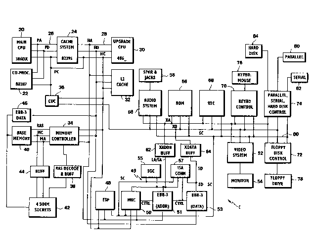
Referring now to Figure 1, the letter C designates
generally a computer system incorporating the present
invention. System C is comprised of a number of block
elements interconnected via four buses. Throughout
this specification, an asterisk following the signal
mnemonic indicates that the signal may be active at a
logic low level and always is the inverse of a signal
mnemonic without the asterisk. Signal mnemonics having
numbers or ranges between angle brackets refer to those
particular bits or positions in a bus.
A main CPU 20 is connected to a numeric
coprocessor 22 and to a cache system 24. A bus,
generally referred to as the P or processor bus 26 is
used to connect the main CPU 20, the numeric
_oprocessor 22 and the cache system 24. Preferably the
main CPU 20 is an Intel Corporation 80386 DX-25
microprocessor, while the numeric coprocessor is an
80387 and the cache system 24 is an 82395 cache
controller. Preferably the 82395 is used as its back
end interface is similar to and compatible with the 486
variations. A second or H or host bus 28 is used to
connect the cache system 24 to various other elements
in the computer system C. For example, an upgrade CPU
socket 30 is provided to receive various upgrade
sockets of the 486 family developed by Intel. A level
2 or secondary cache 32 is also connected to the host -
bus 28 for operation. It is understood that the
various buses such as the P bus 26 and the host bus 28 -~
are generally comprised of three portions: an address
20 portion, a data portion, and a control portion, such as ;
the PA, PD and PC buses or the HA, HD and HC buses.
The main CPU 20 and the upgrade socket 30 are also
connected to a CPU utility control (CUC) circuit 36 by
the PC bus and the HC bus. The CUC 36 is connected to
an X data bus 60, which is a form of an input/output
(I/0) bus in the computer C. The CUC 36 performs
miscellaneous CPU control and interface functions.
In the preferred embodiment a memory controller 34
is connected to the host bus 28 to provide control of
the memory utilized in the computer system C.
Describing now the memory portion of the computer
system C, the memory controller 34 provides control
signals to a row address strobe (RAS) decode and buffer
unit 38 which is connected to the memory controller 34.
The memory controller 34 is also connected to base
~ 3
memory 40 by a memory or M bus. Preferably the base
memory 40 is developed by using a plurality of dynamic
random access ~emories (DRAMs) which are conventionally
601dered to the circuit board. Memory sockets 42 are
preferably designed to receive single in-line memory
modules (SIMMs). The RAS outputs from the RAS decoder
38 are provided to the memory sockets 42. The memory
controller 34 provides the memory control NC and memory
address MA signals to the base memory 40 and to buffers
44 which are in turn connected to the memory sockets
42. Data signals are conveyed to the memory sockets 42
and the base memory 40 by an EISA bus buffer (EBB) 46
connected to the HD bus.
In the preferred embodiment, the computer system C
utilizes an ISA external bus, designated as the S bus
49 in Figure 1. A bus controller 50 referred to as the
MBC provides certain of the necessary control functions
between the H bus 28 and the S bus 49 and provides the
S bus control or SC lines. Connected to the M3C 50 is
the EISA system peripheral (ESP) circuit 48, which is
compatible with an ISA bus system and includes various
timers, the direct memory access (DMA) controller and
the interrupt controller logic of the computer system
C. The MBC 50 controls an address EBB 51 connected to
the HA bus to develop the LA and SA address lines and a
data EBB 53 connected between the HD bus and the SD bus
to develop the SD lines. Connected to the S bus 49 is
are the ISA connectors 57 to receive option circuit
boards.
~eveloped from the S bus 36 is the fourth and
remaining bus referred to as the X bus 60. The X bus
is developed by means of a system glue chip (SGC) 55
which is connected to the S bus 49 and, performs
numerous address decoding operations. The SGC 55
35 controls a buffer 62 connected to the SA lines to ;
, i.. ~ ~.. ,3
~ develop the XA address lines and a buffer 64 provided
.1 between the SD lines and the XD lines. The SC control ::
lines are used directly to help control the X bus 60.
Various internal components in the computer system C
l 5 are connected to the X bus 60. For example, the read
.1 only memory or ROM 66 containing the BIOS of the ~ ~:
!~ computer system C is connected to the X bus 60 as are
the real time clock (RTC) nnd CMOS memory 68, a
keyboard controller 70, a floppy disk controller 72 and
a multiple peripheral controller 74. A video system 52
is connected to the X bus, with a monitor 54 connected
to the vide~ system 52 to provide a graphic output for
the computer system C. Additionally, an audio system ~:~
56 is connected to the X bus 60, with an internal
speaker and jacks 58 for external amplifiers and
speakers connected to the audio system 56. The
keyboard controller 70 is connected to a keyboard and a ~ :
mouse system 76 to provide user input while the floppy
disk controller 72 is connected to a floppy disk drive
78. The multiple peripheral controller 74 contains a
parallel port which is connected to a parallel
interface 80, a serial port which is connected to a
serial interface 82 and a hard disk interface which is
connected to a hard disk unit 84.
The computer system C shown in Figure 1 is . ~
exemplary of a computer system incorporating the :~ :
present invention and numerous other variations could
of course be developed as obvious to one skilled in the
art.
The computer system C of the preferred embodiment
is compatible with four types of upgrade ~:
microprocessors manufactured by Intel: the 486SX, the
487SX, the 486DX and 486DX2. For purposes of this
discussion any references to 486DX will also include a
reference to the 486DX2 as the pin arrangements are
. .
~ ' .
z
J
.
identical. Each microprocessor type includes a family
of microprocessors having various performance
characteristics and qualities, but sharing the same
basic design and pin arrangement. As sho~n in Figs.
i 5 ~A, 2B and 2C and Table 1 ~elow, each of the three
types of upgrade microprocessors shares a common pin
arrangement but for 5 pins. The connections of these 5
pins to the various signals of the computer system must
be changed according to the particular type of
microprocessor used.
able 1
Socket Pin Signal
Number
486SX 487SX 486DX
A13 NC FERR* NC
A15 NMI IGNNE* IGNNE*
B14 NC UPGRADE* NC
B15 NC NMI NMI
25C14 NC NC FERR*
:~;
Pin A13 generates the FERR* (Eloating Point Error)
signal on the 487SX chip. The asterisk (*) indicates
that the signal is asserted LOW and negated ~IGH. When
asserted LOW, the FERR* signal indicates that a ;~
floating point error has occurred. The FERR* signal is
supplied to the CUC 36. In the 486SX and 486DX
microprocessors, pin A13 is not used, and should be
unconnected.
For the 486DX microprocessor, the FERR* siqnal is
generated on pin C14. Pin C14 is not used, however, on
the 486SX and the 487SX microprocessors, and is thus
not connected for those microprocessors.
Pin B15 receives the NMI (Non-Maskable Interrupt)
signal from the computer system on the 487SX and the ~-
.': :'
. :~
: .
`i 10 -:
486DX microprocessors. The N~I signal ~8 generated by
:~ the ESP 48 and is supplied to the upgrade 60cket. When
asserted HIGH, the NMI signal indicates that a
potentially fatal error has occurred in the system.
This interrupt cannot be disabled and will always be
serviced if active. Pin B15 is not used in the 486SX
microprocessor, and therefore remains unconnected.
For the 486SX microprocessor, pin A15 receives the
NMI signal. For the 487SX and 486DX microprocessors, -
on the other hand, pin A15 should receive the IGNNE*
(Ignore Numeric Error) signal. The IGNNE* signal is
asserted LOW and negated HIGH. The IGNNE* signal, when
asserted LOW by the CUC 36, instructs the processor to
ignore a numeric error and continue executing floating
point instructions. When the IGNNE~ signal is negated
HIGH, the processor freezes a non-control floating
point instruction if a previous floating point
instruction caused an error. The IGNNE* signal is not
used by the 486SX microprocessor.
Pin B14 is an extra pin used only on the 487SX
microprocessor. Pin B14 generates the UPGRADE* signal,
which is asserted LOW and negated HIGH. When asserted ~ ~
LOW, the UPGRADE* signal indicates to the various f
system components that a processor is present in the
upgrade socket. The pin at the B14 location on the
486SX and 486DX microprocessors is not connected.
Referring now to Fig. 3, a computer system
according to the present invention includes th~ upgrade
socket 30 that can receive any of the upgrade
microprocessor types. In the preferred embodiment, a
set of switches 160, 162, and 164 control the routing
of signals to and from pins A13, C14, B14, B15 and A15. -
Each switch 160, 162 and 164 is a 2 position,
preferably surface mount, switch. The switch 160
controls the routing of pin C14. As described above,
,
'~
''~
h~
,, ;" `, ~ 'j? i ~ ,
Z pin C14 should be unconnected for the 486SX and the
487SX microprocessors, but generates the FERR* signal
of the 486DX microprocessor. One side of the switch
1 160 is connected to ground, and the other cide is
! 5 connected to a resistor 166. The other Qnd of the
resistor 166 is connected to a 5 volt ~upply 80 that
when ~witch 160 is open, a HIGH signal i8 generated at
the node between the resistor 166 and the switch 160.
The resistor 166 and the ~witch 160 are connected to
10 the inverted enable input of a non-inverting tri-state
buffer 168. If enabled, the buffer 168 allow5 a signal
to pass through the buffer 168. If the buffer 168 is
not enabled, the buffer 168 is in a tri-state mode and
acts like an open circuit. The input of the buffer 168
15 is connected to pin C14 and the output of the buffer
168 is connected to the FERR* input of the CUC 36. The
buffer 168 is enabled by a LOW signal at its enable
input. Thus, when the switch 160 is closed, a LOW
signal is asserted at the enable input of the buffer
20 168, connecting the pin Cl4 of the microprocessor to
the FERR* signal. Therefore, when a 486DX
microprocessor is used, the ~witch 160 should be
closed. Otherwise, the switch 160 should be open,
leaving pin C14 unconnected.
Similarly, a switch 162 controls the routing of
pin B14 and the UPGRADE* signal. One end of the switch -~
162 is connected to ground, and the other end of the
switch 162 is connected to a resistor 170. The
resistor 170 is connected to the 5 volt supply. The
resistor 170 and the switch 162 are connected to the
inverted enable input of a non-inverting tri-state
buffer 171 identical to the buffer 168 described above.
The input of the buffer 171 is connected to pin B14 of
the upgrade socket 30, and the output of the buffer 171
is connected to the UPGRADE* signal. Pin B14 is also
12
connected to a pull-up resistor 177 connected to the 5
volt ~upply to generate a HIGH 6ignal when the buffer
171 is activated but pin 814 of the Focket 30 i6 not
connected. The resistor 170 and the switch 162 are
also connected to the non-inverted enable lnput of a
second non-inverting tri-state buffer 179, having its
input connected to ground and its output connected to
the UPGRADE* signal. When the switch 162 is closed, a
LOW signal is asserted at the enable input of each
buffer 171, 179, enabling the first buffer 171 and
connecting pin B14 to the UPGRADE* signal. If a 487SX
microprocessor is in the socket 30, the UPGRADE* signal
is asserted LOW. If anothar processor is in the socket
30 or the socket 30 is empty when the switch 162 is
closed, the UPGRADE* signal is pulled HIGH by the pull~
up resistor 177. On the other hand, when the switch -
162 is open, a HIGH signal is asserted at the enable
input of each buffer 171, 179. Consequently, the
second buffer 179 is enabled so that the UPGRADE*
signal is connected to ground, asserting a LOW signal.
Because the UPGRADE* signal should be LOW when an -
upgrade microprocessor is in the socket 30, the switch
162 should be opened when a 486SX or a 486DX is -
inserted. On the other hand, the switch 162 should be -~
closed when the socket 30 is empty. If a 487SX ~
microprocessor is positioned in the socket 30, the ~ -
switch 162 should be closed because pin B14 of the
487SX processor generates a LOW value on the UPGRADE*
signal when the processor is properly placed, and is
preferred to remain closed for reasons indicated below.
Similarly, the switch 162 and another switch 164
control the routing of pin A13 of the upgrade socket
30. Pin A13 should be connected to the FERR* input of
the CUC 36 when used with the 4875X microprocessor, and
is not connected for the 486SX and 486DX
13
microprocessors. One end of the switch 164 is
connected to ground. The other end of the switch 164
is connected to a resistor 174, which is in turn
~onnected to the 5 volt supply. The resistor 174 and
the switch 164 are connected to a first input of a 2-
input OR gate 175, and the r~sistor 170 and the switch
162 are connected to the other input. The output of
the OR gate 175 is connected to the inverted enable
input of a non-inverting tri-stateable buffer 172. The
input of the buffer 172 is connected to pin A13 of the
CPU socket 30, and the output of the buffer 172 is
connected to the FERR* signal. When both switches 162,
164 are closed, a LOW signal is asserted at the enable
input of the buffer 172, connecting pin A13 to the
15 F~RR* siqnal. Because pin A13 should only be connected -~
to the FERR* signal if the 487SX microprocessor is
used, both of the switches 1~2, 164 should be closed
only if a 487SX microprocessor is in the ~ocket 30. ~; ~
A pull-up resistor 173 is connected between the 5 - --
volt supply and the FERR* input of the CUC 36 so that
no error signal is provided when switches 160 and 162
are both open, as when a 486SX microprocessor is
installed or as may accidentally occur. Therefore the
FERR* input is at a known level in all cases and does
not float.
The switch 164 also controls the routing of
signals to pin B15 and pin A15 of the CPU socket 30.
The switch 164 and the resistor 174 are connected to
the inverted enable inputs of 2 non-inverting tri-state
buffers 176 and 178 and to the input of an inverter
180. The output of the inverter 180 is connected to
the inverted enable input of another non-inverting tri-
state buffer 182. According to this arrangement, when
the first two buffers 176 and 178 are enabled, the -
35 third buffer 182 will be disabled, and conversely, when ~-
, ~ ~ 3
the third buffer 182 is enabled, the fir~t two buffers
176 nnd 178 will be disabled. When the switch 164 i5
closed, the first two buffers 176 and 178 are enabled,
and ~hen the switch 164 is opened, the buffer 182 is
S disabled. The input of the first buffer 176 is
connected to the NMI signal, and its output i6
connected to pin B15. The input of the second buffer ~ -`
178 is connected to the IGNNE* signal, and its output
is connected to pin A15. Therefore, when switch 164 is
10 closed, pin B15 receives the NMI signal and pin A15 is ~-
connected to the IGNNE* signal.
When the switch 164 is open, however, the first
two buffers 176 and 178 are disabled. Therefore, pin ~ -~
B15 is not connected. Pin A15, however, is connected ~-
to the output of the third buffer 182, which is
enabled. The input of the third buffer 182 is
connected to the NMI signal. When the 486SX ~-
microprocessor is being used, pin B15 should be
unconnected and pin A15 should be receiving the NMI
20 signal. When a 487SX or a 486DX microprocessor is
being used, pin B15 should receive the NMI ~6ignal, and
pin AlS should receive the IGNNE* signal. Therefore, --~
for the 486SX microprocessor the switch 164 should be `
opened, and should be closed for the 487SX or the 486DX
microprocessors.
When no upgrade processor is used, switch 160
should be open or off, switch 162 should be closed or
on and switch 164 should be open or off. This setting
of switch 160 results in buffer 168 being tri-stated.
30 These settings of switches 162 and 164 result in buffer
172 and buffer 179 being tri-stated and buffer 171
being activated, but the UPGRADE* signal is pulled high
by the resistor 177, as an 487SX is not present. Thus
these settings effectively disable the switched outputs
35 from the upgrade socket 30. ~ ;
_ :
- 2
r.l .L ~ 3
Tnble 2 below illustrates the proper ~ettings of :
the switches 160, 162 and 164 for the three
microprocessors, and for use when an upgrade :~
microprocessor is not present and the ~ain CPU 20 is
controlling the computer system C.
Table 2
Switch Signal
386DX 486SX 487SX 486DX ~:
, .~ ".
160 OFF OFF OFF ON ~ :
162 ON OFF ON OFF :
5 164 OFF OFF ON ON
When these three switches are properly set, any of
the three upgrade processors may be used in the socket
~0 30 or none may be used. If an upgrade processor is
placed in the system, the UPGRADE* signal is asserted
LOW. The UPGRADE* signal is asserted LOW and negated
HIGH, and indicates to ~pecific components when the
system has been upgraded. Referring now to Figure 4,
25 the UPGRADE* signal is provided to the input of an ~-
inverter 190 and one input of a 2-input ~ND gate 192.
A FLUSH* signal, connected to the upgrade socket 30, is ~ ;~
connected to the other input of the AND gate 192. The :~
FLUSH* signal is generated by the CUC 36 when the
30 computer system C wishes to invalidate the contents of ~:
the 82395 cache 24 or the cache on the upgrade
processor. In this instance however, the FLUSH* input
of the cache system 24 using an 82395 is also used in
conjunction with the SAHOLD (System Address HOLD) ~:~
35 signal to place the cache system 24 in its tri-state :-~
test mode as described below. Therefore, the output of
the inverter 190 is connected to the SAHOLD input of
the 82395 cache system 24, and the output of the AND
gate 192 is connected to the FLUSH* input of the 82395
.... ~ , ...
16
cache system 24. The FLUSH* signal, generated by the
CUC 36 in response to processor commands, and the
UPGRADE* signal are used to put the 82395 in the cache
system 24 in its tri-state test mode, ~llowing the
upgrade microprocessor to control the system, as
described below. The UPGRADE~ signal may also be ~ ~
provided to other system components to ~ndicate that -
the upgrade microprocessor has been inserted.
When the three switches are properly set, the
UPGRADE* signal is asserted LOW whenever an upgrade
microprocessor is plugged into the socket 30. To allow ~ ~
the upgrade microprocessor to control the host bus, the - ~-
82395 in the cache system 24 must be placed in its tri-
state test mode. As described below, the cache
system's SAHOLD and FLUSH* inputs must both be asserted
to cause the cache system 24 to enter test mode, so the
inverted UPGRADE* signal is connected directly to the
SAHOLD input. In addition, the UPGRADE* signal is
ANDed with the FLUSH* signal so that the output of the
AND gate 192 follows the FLUSH* signal if UPGRADE* is
negated, but is held LOW when UPGRADE* is asserted.
The AND gate 192 output is provided to the cache
system's FLUSH* input, which allows the 82395 in the
cache system 24 to be placed in test mode whenever an ~-
25 upgrade processor is present. In an alternative -
embodiment, the AND gate may be replaced by a
programmable logic array (PAL) that performs the same
function as the AND gate 192 and also allows
development of a properly timed FLUSH* signal to allow
testing of the memory in the 82395.
To place the 82395 cache system 24 into test mode,
the SAHOLD and FLUSH* inputs must be asserted during
the falling edge of a reset signal. Therefore, when an
upgrade microprocessor has been plugged in, the system
can be power cycled to reset it. When an upgrade
r ~ ;v i ~
~ .
17
processor is present, the UPGRADE* signal is
~ automatically generated, which is inverted ~nd
¦ connected directly to the SAHOLD input o~ the cache
system 24. In addition, the UPGRADE* signal holds the
¦ S cache system's FLUSH* input LOW through the AND gate
122. As a result, the 82395 cache system 24 enters
test mode at the falling edge of the RESET signal,
floats its outputs, and does not respond to normal
system signals. The cache system 24 remains in test
mode until the system is reset with SAHOLD and FLUSH*
driven inactive. Consequently, the upgrade processor
controls the host bus without interference from the
82395 cache system 24 as long as the upgrade processor
remains in the socket 30.
lS On the other hand, when the socket 30 is empty,
and the switches 160, 162 and 164 are properly set, the
main CPU 20 controls the system and the cache ~ystem
operates normally. Without an upgrade processor,
UPGRADE* is negated, and the SAHOLD input remains LOW.
In addition, the output of the AND gate follows the
FLUSH* signal. Thus, when system is reset, the cache
system 24 flushes normally and continues to function.
Upgrading the present system is simple. When the --
system is powered down, the upgrade microprocessor is --
placed in the upgrade socket 30. To provide the
correct signal routing, the switches 160, 162 and 164 ~ -
are set according to the above disclosure in accordance
with the type of upgrade processor used. Then the ---~
system is powered up. As the main CPU 20 begins its~
power-on sequence, it addresses the cache system 24,
calls for a startup vector, and waits until an answer
is received. Until the cache system 24 responds, the -~
main CPU 20 suspends operations and waits. - ~
Consequently, the main CPU 20 interacts with no other ~ -
35 system components until the cache system 24 provides ~
. ~. ~:
. .'''.'''''',' ~,
.~,... ..
'7`~?
Jf~
.
18
the startup vector. As described above, however, the
cache ~ystem 24 is "asleep" and does not r~spond. The
upgrade processor, on the other hand, is reset and is
connected to the host bus. Because the upgrade
processor does not rely on the cache system ~4 for its
startup vector, the upgrade processor commences
operations and functions as if the main CPU 20 were
¦ absent. Thus, the cache system 24 remains "asleep",
the main CPU 20 operations are suspended, and the
upgrade processor controls the computer system.
Because most of the cache system 24 host bus
interface is identical to the host bus interface of the
I upgrade microprocessor, most of the signals on the
¦ cache system 24 may be connected directly to the
corresponding signals on the upgrade socket 30.
Nonetheless, the upgrade host bus and the cache system
host bus interface cannot be entirely tied together,
because the main CPU 20 uses the processor bus for
certain signals that, if tied directly to the
corresponding signals of the upgrade socket 30 on the
host bus, would cause errors and degrade the
perfor~ance of the cache system 24. As a result, some
of the signals must be multiplexed and ~witched between
the upqrade socket 30 and the preferabl~ 80386 main CPU
20 and the preferable 80387 co-processor 22. Because
the timing of some of these signals is critical,
however, the signals generated by many conventional
EISA chip sets cannot be effectively switched to the
upgrade socket 30 with active components.
Consequently, the signals in the present embodiment are
rerouted manually using a set of six switches.
Alternatively, zero delay logic controlled switches
similar to relays could also be utilized, with the
switching based on the UPGRADE* signal. It should be
noted, however, that the system may be redesigned using
`~j
,J
! ~ 19
application specific integrated circuits (ASIC5) to
ccmpensate for the timing anomalies 80 that the
;i~ switching and multiplexing may be performed
i' electronically.
~ 5 Referring now to Figure 5, the NBC 50 generates
J the HHOLD (Host bus Hold) signal, which is connected to
a first manual switch 200. The other terminal of the
switch is connected to the HOLDI input of CUC 36 and a
~I pull-dow~ resistor 202. The HOLDI input on the CUC 36
i 10 is used to interface with hold logic inside the CUC 36
i for architectures where the processor is located
directly on the host bus 28. The HHOLD signal is
asserted when another master must have the host bus,
and must be provided to the HOLDI input of the CUC 36
when an upgrade microprocessor is beinq used.
Therefore, the switch 200 is open when the upgrade
socket 30 is empty, holding the HOLDI input at a LOW ~
level. On the other hand, when an upgrade processor is ~-
inserted, the switch 200 is closed, allowing the MBC 50
to provide the HHOLD signal to the HOLDI input of the
CUC 36. The PLOCK* signal from the main CPU 20 is
provided to a non-inverting buffer 201 whose non-
inverted enable input receives the UPGRADE* signal. ~- -
The output of the buffer 201 is pulled up to 5V by a ~ -
resistor 203 and is connected to the PLOCR* input of
the CUC 36. Thus when no upgrade microprocessor is ~ -
used, the PLOCK* signal is provided to the CUC 36, but
the PLOCK* input of the CUC 36 is pulled up or inactive
when an upgrade processor is present. The PLOCR*
signal is used in conjunction with the HHOLD input of
the CUC 36 to allow modification of processor lock
cycles if desired. In this manner, the CUC 36 receives
either the PLOCK* signal at the PLOCK* input or the
HHOLD signal at the HOLDI input, allowing the desired
control of locked cycles. A buffer 201 can be used
. ~ -~
., ~
wit~ the PLOCK* signal as it is not as timing critical
as the HHOLD signal in the preferred embodi~ent.
Both the main CPU 20 and the upgrade ~ocket 30
include HLDA (Hold Acknowledge) outputs. When a hold
S request is asserted, the controlling proce~sor responds
~- by asserting the HLDA signal, indicating that the
processor has given the bus to another system bus
master. To allow the correct processor to assert the
HLDA signal, a switch 204, 206 is connect~d between -
~ 10 each of the processor's HLDA outputs and the PHLDA
3 (Processor Hold Acknowledge) input of the CUC 36.
Consequently, if the upgrade ~ocket 30 is empty, the
' switch 204 between the upgrade socket 30 and the PHLDA
j input is open, and the switch 206 between the main CPU
¦ 15 20 and the PHLDA input is closed. Conversely, when an
upgrade processor has been plugged into the socket 30,
the upgrade socket switch 204 is closed and the main
CPU switch 206 is open.
Similarly, both the main CPU 20 and the upgrade
20 socket 30 provide an ADS* (Address Status) output
signal to indicate that a valid address is on the
address bus. In the present system, the proper ADS*
signal must be provided to the PADS* tProcessor Address
Status) input of the CUC 36. The CUC 36 uses this
25 input to provide a ready indication during certain
special cycles and conditions. Therefore, a switch 208
is provided between the main CPU 20 ADS* output and the
PADS* input, and another switch 210 controls the
connection between the upgrade socket 30 ADS* output
30 and the PADS* input. ~f an upgrade processor is in the
upgrade socket 30, the upgrade switch 210 is closed and
the main CPU switch 208 is open, and vice versa if the
upgrade socket 30 is empty.
Finally, the numeric co-processor 22 generates an
35 ERROR* signal to indicate an error condition from the
21
numeric co-processor extension. When the upgrade
socket 30 is empty, the ERROR* signal i~ provided to
the CUC 36 through a closed switch 212. Si~ilarly, the
487SX and 486DX microprocessors generate a FERR* signal ~-
¦ 5 when floating pointing errors occur, which signal is ~ -
routed as described above, relating to buffers 168 and
¦ 172, to develop the FERR* signal shown illustratively
¦ in Fig. 5. Therefore, the main CPU switch 212 must be
open if an upgrade processor is present. Unlike the
upgrade socket HLDA and ADS* outputs, no switch
controls the connection between the FERR* signal from
the upgrade socket switching logic and the CUC 36.
When no upgrade processor is present both buffers 168
and 172 are disabled, so no signal is being provided on
the FERR* line. Additionally, if no upgrade processor
is present and switch 212 is closed, but a numeric co~
processor 22 is also not present, the resistor 173
pulls up the FERR* input to the CUC 36.
As noted above, the CUC 36 can be redesigned to
20 automatically handle the switching performed by the `
switches 200, 204, 206, 208, 210 and 212 by using the
UPGRADE* signal and to resolve the timing problems, if ---
desired. ;
Therefore systems according to the present
25 invention allow the upgrade of an 80386/82395 system to ~-~
a 486 processor family system without the need for
replacing the system board or even a processor board,
at the small expense of an extra socket and several
switches.
The foregoing disclosure and description of the
invention are illustrative and explanatory thereof, and
various changes in the size, shape, materials,
components, circuit elements, wiring connections and
contacts as well as in the details of the illustrated ;~
: '
22
'~ circuitry and construction may be made ~ithout
departing fr~m the spirit of the inventior.
~
~'',.