Note: Descriptions are shown in the official language in which they were submitted.
~ 211283~
The present invention relates to a control circuit of a
power converter for precisely controlling output voltage from
a power converter which has a plurality of switching devices
and which is capable of obtaining AC conversion output.
Fig. 57 is a block connection diagram equivalent to a
conventional inverter control circuit of a type, for example,
disclosed in "Inverter Output Voltage Waveform Closed Loop
Control Technique", p. 205 to 212, a collection of theses,
FIFTH INTERNATIONAL TELECOMMUNICATIONS ENERGY CONFERENCE
(Oct, 18 to 21, Tokyo), Intelec 83.
Referring to Fig. 57, reference numeral 1 represents a
main inverter circuit, 2 and 3 respectively represent a
reactor and a capacitor which form an AC filter, 4 represents
a DC power source, 5 represents a load, 7 represents a drive
circuit for the main inverter circuit 1, 801 represents an AC
sine-wave reference oscillation circuit, 802 represents an
amplitude command generating circuit and 803 represents a
voltage control amplifier. Reference numeral 804 represents
a pulse-width modulation circuit (hereinafter called a "PWM
circuit") comprising, for example, a comparative circuit 804a
and a
- 1 -
211283~
carrier wave generating circuit 804b as shown in Fig. 58.
Reference numeral 811 represents a multiplier and 812
represents an adder/subtracter.
The operation of the circuit shown in Fig. 57 will now be
described.
A portion of the circuit between the terminals of the
capacitor 3 thereof enables output voltage to be obtained, the
level of which corresponds to control output PWMO from the PWM
circuit 804. On the other hand, the output from the AC sine-
wave reference oscillation circuit 801 and that from the
amplitude command generating circuit 802 are multiplied in the
multiplier 811 so that output voltage command Vc* is made.
Then, the deviation between the output voltage command Vc* and
output voltage Vc is calculated by the adder/subtracter 812.
The voltage control amplifier 803 and the PWM circuit 804
control the switching operation of the inverter l to make the
foregoing voltage deviation to be zero.
Since the conventional apparatus for controlling the
power converter, such as the inverter, has been constituted as
described above, there arises the following problems.
(1) The main inverter circuit l is operated as a very
low impedance voltage source when viewed from the output side
thereof. Therefore, a problem of short circuit sometimes rises
on the load side of the main inverter circuit 1. Another
-2-
2112830
problem arises if an in-rush current flows due to a supply of
transformer voltage in that an excess flow of the output
electric current easily realizes an excess current state and
therefore protection of circuit elements becomes difficult.
(2) Since the voltage control system of the main
inverter circuit 1 includes an LC filter having an
unsatisfactory damping characteristic, the voltage control
amplifier 803 cannot easily be so designed as to prevent the
resonance of the foregoing filter to stabilize the voltage
control system.
(3) Since the reactor 2 is, in series, connected to the
output terminal of the main inverter circuit 1 and the voltage
drop of the reactor 2 is changed to follow the electric current
flowing through the load 5, there arises a necessiky for the
voltage control amplifier 803 to completely and quickly
compensate the foregoing voltage drop in order to control the
output voltage to be a desired value. Therefore, even if no
precise output voltage is needed, the output voltage control
performed by the voltage control amplifier 803 is needed to
compensate the voltage drop in the reactor 2. If precise
output voltage is needed, the design must be so made that the
voltage control ampli~ier 803 has a large gain. However, ~he
stability of the voltage control system limits the gain
enlargement, and therefore overshoot or undershoot of the
output voltage corresponding to the response of the voltage
-3-
2~12830
control system undesirably takes place if the load has beenchanged rapidly.
The present invention overcomes or at least mitigates
the foregoing problems and provides an apparatus for
controlling a power converter with which the power converter
and the output line can easily be protected from an excess
current.
The present invention provides a control apparatus for
controlling a power converter which is able to improve the
apparent damping factor of an LC filter, with which the
design of a voltage control amplifier is facilitated, which
is able to compensate voltage drop of a serial reactor at
speed higher than the response of a voltage control system to
improve the output voltage characteristic and with which the
converter and the output line can easily be protected from
excess currents.
A control apparatus for controlling a power converter
according to the present invention comprises: voltage
commanded value generating means for generating a voltage
command value to command voltage to be transmitted from the
power converter; voltage control means for controlling a
plurality of switching devices of the power converter in
accordance with a commanded voltage level; electric current
detection means for detecting an output electric current to
be supplied from the power converter to the load; and
electric current limiting means for restricting the commanded
voltage level to be supplied to the voltage control means in
accordance with a value detected by the electric current
detection means.
- 4 -
211283~
The invention will be further described by reference to
the accompanying drawings, in which:
Fig. 1 is a block diagram which illustrates a first
embodiment of the present invention;
Fig. 2A is a block diagram which illustrates a circuit
of a power converter (a main inverter circuit) for use in the
present invention;
Fig. 2B is a block diagram which illustrates a circuit
of another power converter for use in the present invention;
Fig. 3 is a graph which illustrates the characteristics
of transfer functions G (S) 807 and Z (S) 822;
Figs. 4 to 35 are block diagrams which respectively
illustrate second to thirty-third embodiments;
Fig. 36 is a block diagram which illustrates the
principle of the operation of the thirty-third embodiment;
Figs. 37 to 55 are block diagrams which respectively
illustrate thirty-fourth to fifty second embodiments;
Fig. 56 is a circuit diagram which illustrates another
embodiment of the converter according to the present
invention;
Fig. 57 is a block diagram which illustrates the
structure of a conventional system; and
Fig. 58 is a block diagram which illustrates the
structure of a PWM circuit shown in Fig. 57.
-- 5
~ 28~
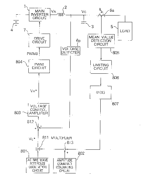
First Embodiment
Fig. 1 illustrates a first embodiment of the present
invention. Referring to Fig. 1, reference numeral 1
represents a main inverter circuit exemplified by a circuit
for, with triangle-wave carriers of about 1 to 2 KHz,
modulating the pulse width of a single-phase full bridqe
inverter having transistors Sl to S4 which diodes D1 ~o D4
disposed as shown in Fig. 2a are inversely connected in
parallel. Reference numerals 2 and 3 respectively represent
a reactor and a capacitor for a filter, 4 represents a DC
power source, 5 represents a load, 7 represents a drive
circuit for the main inverter circuit 1, 6a represents a
detector for detecting load current IL, and 6c represents a
voltage detector for detecting output voltage Vc.
Referring to Fig. 1, reference numerals between eight
and nine hundred represent elements of a control circuit.
Reference numeral 801 represents an AC sine-wave reference
oscillation circuit, 802 represents an amplitude command
generating circuit, 803 represents a voltage control
amplifier, 804 represents a PWM circuit, 805 represents a
mean value detection circuit, 806 represents limiting
circuit, 807
21I2830
represents a transfer function G (S), 811 represents a
multiplier, and 812 and 813 represent adders/subtracters.
If a function having, for example, a non-linear
characteristic, with which the output is multiplied by
coefficient times with respect to the input while limiting the
same below a certain level, is used as the transfer function G
(S) 807, the output voltage is dropped in proportion to a small
input. If a large input is received, the amount of the drop of
the voltage is limited.
The operation of the thus-constituted first embodiment
will now be described with reference to Fig. 1. In order to
make output voltage command Vc*, which is the output from the
multiplier 811, coincide with output voltage Vc detected by the
voltage detector 6c, the voltage control amplifier 803 and the
PWM circuit 804 form a voltage control loop so that the
switching operation to be performed by the main inverter _~
circuit 1 is controlled.
Load current IL is detected by the detector 6a, and a mean
load electric current value is detected by the mean value
detection circuit 805. The limiting circuit 806 has a maximum
load current set thereto so that the output from the limiting
circuit 806 is zero if the mean load current value is smaller
than the predetermined value. If the mean load current value
is larger than the predetermined value, a value obtained by
211283~
subtracting the predetermined value from the mean load current
value is transmitted from the limiting circuit 806.
The output from the limiting circuit 806 is passed
through the transfer function G (S) 807 as to be subtracted
from the output transmitted by the amplitude command generating
circuit 802 in the adder/subtracter 813. The output from the
adder/subtracter 813 and that from the AC sine-wave reference
oscillation circuit 801 are multiplied in the multiplier 811 so
that the output voltage command Vc* is obtained. Therefore,
the output voltage command Vc* is dropped if the mean load
current value is larger than the predetermined value set to the
limiting circuit 806. Further, the foregoing voltage control
loop causes the output voltage Vc to be also dropped to follow
the output voltage command Vc*. If the output voltage Vc has
been dropped, also the load current IL is decreased. As a
result, the output line can be protected from an excess
electric current.
That is, when the inverter is viewed from the output side --
thereof, the transfer function G (S) 807 is operated as to be a
virtual output impedance to drop the output voltage Vc only
when the load current IL larger than the predetermined value
has been passed.
Therefore, if the absolute value IG (S)l of the transfer
function G (S) 807 is ~, an excess of the load current IL over =~
the predetermined value due to occurrence of short circuit of a
-8-
211~830
load or the like causes an output impedance ~ to appear
because of the response of the mean value circuit. As a
result, the output voltage Vc is dropped until the load current
IL is made to be smaller than the predetermined value. Since
IG (S)l is finite in actual, the load current IL becomes a
value somewhat larger than the predetermined value. However,
no practical problem arises if the value of the IG (S)l is made
to be a sufficiently large value.
The transfer function G (S) 807 may be an arbitrary
function if it has an adequate impedance value. If the circuit
is a proportional circuit for example, it serves as a resistor.
If the same is a differentiating circuit, the transfer function
G (S) 807 serves as a reactor. If the same is an integrating
circuit, it serves as a capacitor. If the same is a
combination circuit of proportional, integrating and
differentiating circuits, it serves as a circuit formed by
combining a resistor, a capacitor and a reactor. Further, a
circuit containing a non-linear element may be employed if it
has an adequate impedance which limits the load current IL.
Second Embodiment -
Fig. 4 illustrates a second embodiment of the present
invention. Elements corresponding to those shown in Fig. 1 are
given the same reference numerals and their detailed
descriptions are omitted here. The difference from the
foregoing first embodiment lies in that the instantaneous value
-
~11283~ -
of the load current IL is used to change the output voltage
command Vc* as to form a virtual output impedance. The
residual structures are the same as those of the first
embodiment.
In the circuit shown in Fig. 4, the instantaneous value
of the load current IL is supplied to the limiting circuit 806.
If the instantaneous value of the load current is larger than a
predetermined positive value or smaller than a predetermined
negative value, a value obtained by subtracting the
predetermined value from the instantaneous value of the load
current is transmitted from the limiting circuit 806. The
output from the limiting circuit 806 is passed through the
transfer function G (S) 807 and subtracted, in the
adder/subtracter 814, ~rom the output voltage command Vc*,
which is the output ~rom the multiplier 811.
Since the second embodiment is arranged in such a manner
that the output voltage command Vc* is instantaneously dropped
if the instantaneous value of the load current IL is larger
than the predetermined value set to the limiting circuit 806,
the load current IL can be, at high speed, limited within a
predetermined value range set to the limiting circuit due to
the response of the voltage control loop.
Third ~mhodiment
Fig. 5 illustrates a third embodiment of the present
invention. Referring to Fig. 5, elements corresponding to
- 1 0-
2112830.
those shown in Fig. 1 are given the same reference numerals and
their detailed descriptions are omitted here. The difference
from the foregoing first embodiment lies in that the
instantaneous value of the load current IL is used to change
PWM voltage command VA* to form a virtual output impedance.
The residual structures are the same as those of the first
embodiment.
In the circuit shown in Fig. 5, the instantaneous value
of the load current IL is supplied to the limiting circuit 806.
If the instantaneous value of the load current is larger than a
predetermined posltive value or smaller than a predetermined
negative value, a value obtained by subtracting the
predetermined value from the instantaneous value of the load
current ls transmltted from the llmlting clrcult 806. The
output from the llmitlng circuit 806 is passed through the
transfer function G (S) 807 and subtracted, in the
adder/subtracter 815, from the output transmitted by the
voltage control multipller 803. The output from the
adder/subtracter 815 is used as the PWM voltage command VA*.
Since the third embodiment is arranged in such a manner
that the PWM voltage command VA* is instantaneously dropped if
the instantaneous value of the load current IL is larger than
the predetermined value set to the limiting circuit 806, the
load current IL can instantaneously be limited within a
211283~
predetermined value range set to the llmiting clrcuit 806 due
to the response of PWM circuit 804.
Fourth Embodiment
Fig. 6 illustrates a fourth embodiment of the present
invention. Referring to Fig. 6, elements corresponding to
those shown in Fig. 1 are given the same reference numerals and
their detailed descriptions are omitted here. The difference
from the foregoing first embodiment lies in that the mean value
of inverter current IA is used to change the output voltage
amplitude command to form a virtual output impedance. The
residual structures are the same as those of the first
embodiment.
Referring to Fig. 6, the inverter current IA is detected
by a detector 6b, while a mean inverter current is detected by
the mean value detection circuit 805. The limiting circuit 806
has a maximum inverter current set thereto so that the output
from the limiting circuit 806 is ~ero if the mean inverter
current, which is the output from the mean value detection
circuit 805, is smaller than the predetermined value. If the
mean inverter current is larger than the predetermined value, a
value obtained by subtracting the predetermined value from the
mean inverter current is transmitted ~rom the limiting circuit
806.
The output from the limiting circuit 806 is passed
through the transfer function G (S) 807 and subtracted, in the
-12-
2112830
subtracter 813, from the output from the amplitude command
generating circuit 802. Since the output from the subtracter
813 and the output from the AC sine-wave reference oscillation
circuit 801 are multiplied in the multiplier 811 to obtain
output voltage command Vc*, the output voltage command Vc* is
dropped if the mean inverter current is larger than the
predetermined value set to the limiting circuit 806. Also the
output voltage Vc is dropped to follow the output voltage
command Vc* by the voltage control loop. If the output voltage
Vc has been dropped, the inverter current IA is decreased.
Therefore, the converter can be protected from an excess
current.
Since the fourth embodiment is structured in such a
manner that the output voltage amplitude command is dropped
if the mean value of the inverter current IA is larger than the
predetermined value set to the limiting circuit 806, the
inverter current IA can be limited in an averaged manner to be
smaller than the predetermined value set to the limiting
circuit 806.
Fifth Embodiment -~
Fig. 7 illustrates a fifth embodiment of the present
invention. Referring to Fig. 7, elements corresponding to
those shown in Fig. 6 are given the same reference numerals and
their detailed descriptions are omitted here. The difference
from the foregoing fourth embodiment lies in that the
-13-
211283Q
instantaneous value of the inverter current IA is used tochange the output voltage command Vc* to form a virtual output
impedance. The residual structures are the same as those of
the fourth embodiment.
Referring to Fig. 7, the instantaneous value of the
inverter current IA is supplied to the limiting circuit 806.
If the instantaneous value of the inverter current IA is larger
than a predetermined positive value or smaller than a
predetermined negative value, a value obtained by subtracting
the predetermined value from the instantaneous value of the
inverter current IA is transmitted from the limiting circuit
806. The output from the limiting circuit 806 is passed
through the transfer function G (S) 807 and subtracted, in the
adder/subtracter 814, from the output voltage command Vc*,
which is the output from the multiplier 811.
Since the fifth embodiment is arranged in such a manner
that the output voltage command Vc* is instantaneously dropped
if the instantaneous value of the inverter current IA is larger
than the predetermined value set to the limiting circuit 806,
the inverter current IA can be, at high speed, limited to a
value range set to the limiting circuit 806 due to the response
of the voltage control loop.
Sixth Embod;ment
Fig. 8 illustrates a sixth embodiment of the present
invention. Referring to Fig. 8, elements corresponding to
-14-
2 112830
those shown in Fig. 6 are given the same reference numerals andtheir detailed descriptions are omitted here. The difference
from the foregoing first embodiment lies in that the
instantaneous value of the inverter current IA is used to
change the PWM voltage command VA* to form a virtual output
impedance. The residual structures are the same as those of
the fourth embodiment.
Referring to Fig. 8, the instantaneous value of the
inverter current IA is supplied to the limiting circuit 806.
If the instantaneous value of the inverter current IA is larger
than a predetermined positi~e value or smaller than a
predetermined negative value, a value obtained by subtracting
the predetermined value from the instantaneous value of the
inverter current IA is transmitted from the limiting circuit
806. The output from the limiting circuit 806 is passed
through the transfer function G (S) 807 and subtracted, in the
adder/subtracter 815, from the output from the voltage control
amplifier 803. The output from the adder/subtracter 815 is
made to be the PWM voltage command VA*.
Since the sixth embodiment is arranged in such a manner
that the PWM voltage command VA* is instantaneously dropped if
the instantaneous value of the inverter current IA is larger
than a predetermined value set to the limiting circuit 806, the
inverter current IA can instantaneously be limited to a
2112830
predetermined value range set to the limiting circuit 806 due
to the response of the PWM circuit 804.
Seventh Embodiment
Fig. 9 illustrates a seventh embodiment of the present
invention. Referring to Fig. 9, elements corresponding to
those shown in Fig. 1 or Fig. 5 are given the same reference
numerals and their detailed descriptions are omitted here. As
contrasted with the first embodiment arranged in such a manner
that only the load current IL is limited and the fourth
embodiment arranged in such a manner that only the inverter
current IA is limited, the seventh embodiment is arranged in
such a manner that the mean value of the load current IL is
used to cause a maximum value selection circuit 809 to select
either a signal for changing the output voltage amplitude
command or a signal for changing the output voltage amplitude
command in accordance with the mean value of the inverter
current IA to form a virtual output impedance. The residual
structures are the same as those of the first embodiment or
the fourth embodiment.
Referring to Fig. 9, the load current IL i5 detected by
the detector 6a, while the mean value of the load electric
current is detected by the average value detection circuit
805a. A limiting circuit 806a has a maximum load current set
thereto. If the means value of the load current, which is the
output from the mean value detection circuit 805a, is smaller
~ 6-
21128~0
than a predetermined value, the output from the limiting
circuit 806a is zero. If the mean value of the load current is
larger than the predetermined value, a value obtained by
subtracting the predetermined value from the mean value of the
load current is transmitted from the limiting circuit 806a.
The output from the limiting circuit 806a is passed
through the transfer function G (S) 807a and supplied to the
maximum value selection circuit 809. On the other hand, the
inverter current IA is detected by the detector 6b, while the
mean inverter current is detected by a mean value detection
circuit 805b. A limiting circuit 806b has a maximum inverter
current set thereto. If the mean value of the inverter
current, which is the output from the mean value detection
circuit 805b is smaller than a predetermined value, the output
from the limiting circuit 806b is zero. If the mean value of
the inverter current is larger than the predetermined value, a
value obtained by subtracting the predetermined value from the
mean value of the inverter current is transmitted from the
limiting circuit 806b.
The output from the limiting circuit 806b is passed
through the transfer function & (S) 807b and re~eived by the
maximum value selection circuit 809. The maximum value
selection circuit 809 selects and transmits a signal that has a
larger absolute value. The output from the maximum value
selection circu~t 809 is, in the subtracter 813, subtracted
-17-
2112830
from the output transmitted by the amplitude command generatingcircuit 802.
The output from the adder/subtracter 813 and that from
the AC sine-wave reference oscillation circuit 801 are
multiplied in the multiplier 811 so that the output voltage
command Vc* is obtained. Therefore, if the mean value of the
load current IL is larger than the predetermined value set to
the limiting circuit 806a or if the mean value of the inverter
current IA is larger than the predetermined value set to the
limiting circuit 806b, the output voltage command Vc* is
dropped. The voltage control loop causes also the output
voltage Vc to be dropped to follow the output voltage command
Vc*. If the output voltage Vc has been dropped, the load
current IL or the inverter current IA is as well as decreased.
As a result, the converter and the output line are protected
from an excess current.
Since the seventh embodlment is arranged in such a manner
that the output voltage amplitude command is dropped if the
mean value of the load current IL is larger than the
predetermined value set to the limiting circuit 80~a or if the
mean value of the inverter current IA is larger than the
predetermined value set to the limiting circuit 806b, the load
current IL and the inverter current IA can be limited in an
averaged manner to be smaller than the predetermined values
respectively set to the limiting circuits 806a and 806b.
~ -18-
2112830
If the predetermlned value to be set to the limiting
circuit 806a is so determined as to be capable of protecting
the output line and if the predetermined value to be set to the
limiting circuit 806b is so determined as to be capable of
protecting the converter, the load current IL can be limited to
a current range in which the output line can be protected and
the inverter current IA can be limited to a current range in
which the converter can be protected.
Although the seventh embodiment is arranged in such a
manner that the limiting circuit 806a and the transfer function
G (S) 807a for forming the virtual output impedance using the
load current IL- and the limiting circuit 806b and the transfer
function G (S) 807b for ~orming the virtual output impedance
using the inverter current IA are individually disposed, the
following common type structure may be employed in a case where
the predetermined maximum current and the virtual output
impedance have the same characteristics: the mean value of the
load current IL and the inverter current IA are supplied to the
maximum value selection circuit 809; and the output from the
maximum value selection circuit 809 is passed through the
limiting circuit and received by the transfer function G (S),
that is, the limiting circuit and the transfer function G (S)
are commonly disposed with respect to the load current IL and
the inverter current IA.
- 1 9-
2112830
Eicrhth Embodiment
Fig. 10 illustrates an eighth embodiment of the present
invention. Referring to Fig. 10, elements corresponding to
those shown in Fig. 9 are given the same reference numerals and
their detailed descriptions are omitted here. The difference
from the foregoing first embodiment lies in that either a
signal for changing the output voltage command Vc* with the
instantaneous value of the load current IL and a signal for
changlng the output voltage command Vc* with the instantaneous
value of the inverter current IA is selected by the maximum
value selection circuit to farm a virtual output impedance.
The residual structures are the same as those of the seventh
embodiment.
Referring to Fig. 10, the instantaneous value of the load
current IL is supplied to the limiting circuit 806a. If the
instantaneous value of the load current IL is larger than a
predetermined positive value or smaller than a predetermined
negative value, a value obtained by subtracting the
predetermined value from the instantaneous value of the load
current IL is transmitted from the limiting circuit 806a. The
output from the limiting circuit 806a is passed through the
transfer function G (S) 807a and received by the maximum value
selection circuit 809. On the other hand, the instantaneous
value of the inverter current IA is supplied to the limiting
circuit 8Q6b.~ If the instantaneous value of the inverter
-20-
2112830
current IA is larger than a predetermined positive value orsmaller than a predetermined negative value, a value obtained
by subtracting the predetermined value from the instantaneous
value of the inverter current IA is transmitted from the
limiting circuit 806b.
The output from the limiting circuit 806b is passed
through the transfer function G (S) 807b and received by the
maximum value selection circuit 809. The maximum value
selection circuit 809 selects a signal having a larger absolute
value ancl outputs it while faithfully restoring the polarity of
the signal. The output ~rom the maximum value selection
circuit 809 is, in the adder/subtracter 814, subtracted from
the output voltage command Vc*, which is the output from the
multiplier 811.
Since the eighth embodiment is arranged in such a manner
that the output vol~age command Vc* is instantaneously dropped
if the instantaneous value of the load current IL is larger
than the predetermine~ value set to the limiting circuit 806a
of if the insta~ntaneous value of the inverter current IA is
larger than the predetermined value set to the limiting circuit
806b, the load current IL and the inverter current IA can
respectively be, at high speed, limited within the
predetermined values respectively set to the limiting circuits
806a and 806b due to the response of the voltage control loop.
-21-
21128~0
Ninth Embodiment
Fig. 11 illustrates a ninth embodiment of the present
invention. Referring to Fig. 11, elements corresponding to
those shown in Fig. 9 are given the same reference numerals and
their detailed descriptions are omitted here. The difference
from the foregoing seventh embodiment lies in that either a
signal for changing the PWM voltage command VA* using the
instantaneous value of the load current IL or a signal for
changing the PWM voltage command VA* using the instantaneous
value of the inverter current IA is selected by the maximum
value selection circuit to form a virtual output impedance.
The residual structures are the same as those of the seventh
embodiment.
Referring to Fig. 11, the instantaneous value of the load
current IL is supplied to the limiting circuit 806a. If the
instantaneous value of the load current IL is larger than a
predetermined posltive value or smaller than a predetermined
negative value, a value obtained by subtracting the
predetermined value from the instantaneous value of the load
current IL 1S transmitted from the limiting circuit 806a. The
output from the limiting circuit 806a is passed through the
transfer function G (S) 807a and received by the maximum value
selection circuit 809. On the other hand, the instantaneous
value of the inverter current IA is supplied to the limiting
circuit 806b. If the instantaneous value of the inverter
-22-
2112830
-
current IA is larger than a predetermined positive value or
smaller than a predetermined negative value, a value obtained
by subtracting the predetermined value from the instantaneous
value of the inverter current IA is transmitted from the
limiting circuit 806b.
The output from the limiting clrcuit 806b is passed
through the transfer function G (S) 807b and received by the
maximum value selection circuit 809. The maximum value
selection circuit 809 selects a signal having a larger absolute
value and outputs it while faithfully restoring the polarity of
the signal. The output from the maximum value selection
circuit 809 is, in the adder/subtracter 815, subtracted from
the output of the voltage control amplifier 803. The output
from the adder~subtracter 815 is made to be the PWM voltage
command VA* .
Since the ninth embodiment is arranged in such a manner ::
that the PWM voltage command VA* is instantaneously dropped if
the instantaneous value of the load current IL is larger than
the predetermined value set to the limiting clrcuit 806a or if
the instantaneous value of the inverter current I~ is larger ~~
than the predetermined value set to the llmiting circuit 806b,
the load current IL and the inverter current IA can
respectively be limited within the predetermined values
respectively set to the llmiting circuits 806a and 806b due to
the response of the PWM circuit 804.
-23-
21I283~
Although the first to ninth embodiments have been
described about the single-phase inverter, the foregoing
arrangement may be applied to a three-phase inverter structured
as shown in Fig. 2b and having transistors S5 to S1o to which
the diodes Ds to D1o are inversely connected in parallel if a
similar control circuit is used for each phase or at least two
phases.
As contrasted with the eighth and ninth embodiments in
which the limiting circuit 806a and the transfer function G (S)
807a for forming the virtual output impedance using the load
current IL and the limiting circuit 806b and the transfer
function G (S) 807b for forming the virtual output impedance
using the inverter current IA are individually disposed, the
following common type structure may be employed in a case where
the predetermined maximum current and the virtual output
impedance have the same characteristics: the instantaneous
values of the load current IL and the inverter current IA are
supplied to the maximum value selection circuit and the output
from the maximum value selection circuit is passed through the
limiting circuit and received by the transfer function G (S),
that is, the limiting circuit and the transfer function G (S)
are disposed commonly to the load current IL and the inverter
current IA.
-24-
21I2830
Tenth Embodiment
A tenth embodiment of the present invention will now be
described. Among multi-phase AC circuits, a three-phase and
three-wire system AC circuit is conditioned that the sum of the
three phase currents is zero. Therefore, the foregoing circuit
has coherency that limiting of a certain phase to a
predetermined value range causes the electric currents of the
residual phases to be so changed as to satisfy the foregoing
condition. As a result, it is difficult to individually
control the three phases.
Fig. 12 illustrates the tenth embodiment of the present
lnvention. Referring to Fig. 12, elements corresponding to
those shown in Fig. 3 are given the same reference numerals and
their detailed descriptlons are omitted here. The difference
from the foregoing second embodiment lies in that a control
circuit is disposed for each phase and an electric current
compensation circuit is additionally disposed so that an
incoherent control is performed.
Referring to Fig. 12, a main inverter circuit 1 is formed
into a three-phase structure as shown in Fig. 2b, wherein
elements having suffix u are elements of a U-phase inverter,
those having suffix v are elements of a V-phase inverter and
those having suffix w are elements of a W-phase inverter. The -~-
instantaneous value of the load current IL for each phase is
supplied to the limiting circuit 806. If the instantaneous
-25
2112830
value of the load current IL is larger than a predetermined
pos~tive value or smaller than a predetermined negative value,
a value obtained by subtracting the predetermined value from
the instantaneous value of the load current IL is transmitted
from the llmiting circuit 806 for each phase.
The output from the limiting circuit 806 is passed
through the transmission function G (S) 807 and received by a
current correction circuit 808. The current correction circuit
808 transmits signals so corrected as to make the sum of the
supplied three-phase signals to be zero. The signals are then,
in adders/subtracters 814u, 814v and 814w, subtracted for each
phase from output voltage commands Vcu*, Vcv* and Vcw*, which
are outputs from multipliers 811u, 811v and 811w.
The detailed operation of the current correction circuit
808 will now be described. Assumptions are made here that the
detected load current values are ILU, ILV, ILW, values set to
the limiting circuit 806 are + K, the outputs from the limiting
circuit 806 are ILUM, ILMV, ILMW and the outputs from the current
correction circuit 808 are IJU, IJV and IJW. If only the U-
phase current has become excessive, the outputs from the
limiting circuit 806 are made as follows:
ILMU = ILU - K (1)
ILMV = O (2)
ILMW = O (3)
- 2 6 -
2112830
The outputs from the current correction circuit 808 are
as follows so that correction is so made that the sum of the
signals of the three phases is made zero and they are
transmitted.
IJU = ILMU ( 4 )
IJV = -- ILMU/2 ( 5 )
IJW = ILMU/2 ( 6)
If electric currents of the two phases, for example, the
U phase and the V-phase, have become excessive, the outputs
from the limiting circuit 806 are made as follows:
ILMU = ILU -- K ( 7 )
ILMV = ILV -- K ( 8 )
ILMW = 0 ( 9)
The outputs from the current correction circuit 808 are
made as follows so that correction is so made that the sum of
the signals of the three phases is made zero and they are
transmitted:
IJU = ILMU ( 11 )
IJV = ILMV ( 12 )
-27 -
211283~ .
IJ~ = -- (LMU + ILMV) ( 13 )
That is, the current correction circuit 808 converts the signal
into a signal with which the sum of the signals of the three
phases adaptable to the three-phase and three-wire system is
made to be zero.
Since the tenth embodiment is arranged in such a manner
that, if any one of the instantaneous values of the respective --
phases of the load current IL has exceeded a predetermined
value set to the limiting circuit 806, a correction signal for
making the sum of the signals of the three phases to be zero is
used to instantaneously drop the commanded output voltage, the
load current IL can be, at high speed and without coherence,
limited to the predetermined value range set to the limiting
circuit 806 due to the response of the voltage control loop.
Eleventh Embodiment
Fig. 13 illustrates an eleventh embodiment of the present
invention. Referring to Fig. 13, elements corresponding to
those shown in Fig. 12 are given the same reference numerals
and their detailed descriptions are omitted here. The
difference from the foregoing first embodiment lies in that the
instantaneous value of the load current IL is used to change
the PWM voltage command to form a virtual impedance. The
residual structures are the same as those of the tenth
embodiment.
-28-
2112330
Referring to Fig. 13, the instantaneous value of the load
current IL for each phase is supplied to the limiting circuit
806. If the instantaneous value of the output current is
larger than a predetermined positive value or smaller than a
predetermined negative value, a value obtained by subtracting
the predetermined vaLue from the instantaneous value of the
load current is transmitted for each phase from the limiting
circuit 805. The outputs from the limiting circuit 806 are
passed through the transmission function G (S) 807 and supplied
to the current correction circuit 808.
The current correction circuit 808 transmits signals so
corrected that the sum of the supplied signals for the three -
phases is zero, the signals being then subtracted, in the
adders/subtracters 815u, 815v and 815w, from the outputs from
the voltage control amplifiers 803u, 803v and 803w. The
outputs from the adders/subtracters 815u, 815v and 815w are
made to be PWM voltage commands VAU*, VAV* and VAW*.
Since the eleventh embodiment is arranged ln such a
manner that, if any one of the instantaneous values of the
respective phases of the load current IL has exceeded a
predetermined value set to the limiting circuit 806, a
correction signal for making the sum of the signals of the
three phases to be zero is used to instantaneously drop the
commanded output voltage, the load current IL can be, at high
speed and withou~ coherence, limited to the predetermined value
-29-
2112~3~ __
range set to the limiting circuit 806 due to the response ofthe PWM circuit 804.
Twelfth Embodiment
Fig. 14 illustrates a twelfth embodiment of the present
invention. Referring to Fig. 14, elements corresponding to
those shown in Fig. 12 are given the same reference numerals
and their detailed descriptions are omitted here. The
difference from the foregoing first embodiment lies in that the
instantaneous value of the inverter current IA is used to
change the output voltage command to form a virtual output
impedance. The residual structures are the same as those of
the tenth embodiment.
Referring to Fig. 14, the instantaneous value of the load
current IL for each phase is supplied to the limiting circuit
806. If the instantaneous value of the output current is
larger than a predetermined positive value or smaller than a
predetermined negative value, a value obtained by subtracting
the predetermined value from the instantaneous value of the
output current is transmitted ~or each phase from the limiting
circuit 806. The outputs from the llmiting circuit 806 are
passed through the transmission function G (S) 807 and supplied
to the current correctlon circuit 808.
The current correction circuit 808 transmits signals so
corrected that the sum of the supplied signals for the three
phases is ~ero, the signals being then subtracted for each
-30-
2112~30
phase, in the adders/subtracters 814u, 814v and 814w, fromoutput voltage commands Vcu*, Vcv* and Vcw*, which are outputs
from the multipliers 811u, 811v and 811w.
Since the twelfth embodiment is arranged in such a manner
that, if any one of the instantaneous values of the respective
phases of the inverter current IA has exceeded a predetermined
value set to the limiting circuit 806, a correction signal for
making the sum of the signals of the three phases to be zero is
used to instantaneously drop the commanded output voltage, the
load current IL can be, at high speed and without coherence,
limited to the predetermined value range set to the limiting --
circuit 806 due to the response of the voltage control loop.
Thirteenth Embodime~
Fig. 15 illustrates a thirteenth embodiment of the
present invention. Referring to Fig. lS, elements
corresponding to those shown in Fig. 14 are given the same
reference numerals and their detailed descriptions are omitted
here. The difference from the foregoing twelfth embodiment
lies in that the instantaneous value of the inverter current IA
is used to change the PWM voltage command to form a virtual
output impedance. The residual structures are the same as
those of the twelfth embodiment.
Referring to Fig. 15, the instantaneous value of the
inverter current IA for each phase is supplied to the limiting
circuit 806. If the instantaneous value of the inverter
-31-
21128~
current IA is larger than a predetermined positive value orsmaller than a predetermined negative value, a value obtained
by subtracting the predetermined value from the instantaneous
value of the inverter current IA is transmitted for each phase
from the limiting circuit 806. The outputs from the limiting
circuit 806 are passed through the transmission function G (S)
807 and supplied to the current correction circuit 808.
The current correction circuit 808 transmits signals so
corrected that the sum of the supplied signals for the three
phases is zero, the signals being then subtracted for each
phase, in the adders/subtracters 815u, 815v and 815w, from
outputs from the multipliers 803u, 803v and 803w. The outputs
from the adders/subtracters 815u, 815v and 815w are made to be
PWM voltage commands VA~*, VAV* and VAW*.
Since the thirteenth embodiment is arranged in such a
manner that, if any one of the instantaneous values of the
respective phases of the inverter current IA has exceeded a
predetermined value set to the limiting circuit 806, a
correction signal for making the sum of the signals of the
three phases to be zero is used to instantaneously drop the PWM
voltage command, inverter current IA can be instantaneously,
without coherence, limited to the predetermined value range set
to the limiting circuit 806 due to the response of the PWM
circuit 804.
-32-
2 11283~
Fourteenth Fmbodiment
Fig. 16 illustrates a fourteenth embodiment of the
present invention. Referring to Fig. 16, elements
corresponding to those shown in Fig. 12 or 14 are given the
same reference numerals and their detailed descriptions are
omitted here. As contrasted with the tenth embodiment
arranged in such a manner that only the load current IL is
limited and the twelfth embodiment arranged in such a manner
that only the inverter current IA is limited, this embodiment
is arranged in such a manner that the maximum value selection
circuit 809 selects the signal for changing the output voltage
command using the load current IL or a signal for changing the
output voltage command using the inverter current IA to form a
virtual output impedance. The residual structures are the
same as those of the tenth or the twelfth embodiment.
Referring to Fig. 16, the instantaneous value of the load
current IL for each phase is supplied to the limiting circuit
806a. If the instantaneous value of the output current is
larger than a predetermined positive value or smaller than a
predetermined negative value, a value obtained by subtracting
the predetermined value from the instantaneous value of the
load current is transmitted from the limiting circuit 806a.
The output from the limiting circuit 806a is passed through the
transfer function G (S) 807a and received by the maximum value
selection circuit 809.
-33-
2112s3a
On the other hand, the instantaneous value of the
inverter current IA for each phase is supplied to the limiting
circuit 806b. If the instantaneous value of the inverter
current IA is larger than a predetermined positive value or
smaller than a predetermined negative value, a value obtained
by subtracting the predetermined value from the instantaneous
value of the inverter current IA is transmitted from the
limiting circuit 806b. The output from the limiting circuit
806b is passed through the transfer function G (S) 807b and
received by the maximum value selection circuit 809.
The maximum value selection circuit 809 selects and
transmits a signal for each phase that has a larger absolute
value. The outputs from the maximum value selection circuit
809 are supplied to the current correction circuit 808 as to be
corrected so that the sum of the signals for the three phases
is made to be zero. The outputs for the respective phases are
then subtracted from the output voltage commands Vcu*, Vcv* and
Vcw* which are the outputs from the multipliers 811u, 811v and
811w, the subtractions being performed in the
adders/subtracters 814u, 814v and 814w.
Since the fourteenth embodiment is arranged in such a
manner that, if any one of the instantaneous values of the load
currents IL for respective phases is larger than the
predetermined value set to the limiting circuit 806a or if any
one of the instantaneous values of the inverter current IA for
-34-
2 11283~
respective phases is larger than the predetermined value set tothe limiting circuit 806b, the correction signal for making the
sum of the signals of the three phases to be ~ero is used to
instantaneously drop the output voltage command, the load
current IL and the inverter current IA can be, at high speed
and without coherence, limited to the predetermined value
ranges set to the limiting circuits 806a and 806b due to the
response of the voltage control loop.
Fifteenth Embodiment
Fig. 17 illustrates a fifteenth embodiment of the present
invention. Referring to Fig. 17, elements corresponding to
those shown in Fig. 16 are given the same reference numerals
and their detailed descriptions are omitted here. The
difference from the foregoing fourteenth embodiment lies in
that the selection circuit 809 selects a signal for changing
the PWM voltage command using the instantaneous value of the
load current IL and a signal for changing the PWM voltage
command using the inverter current IA to form a virtual output
impedance. The residual structures are the same as those of
the fourteenth embodiment.
Referring to Fig. 17, the instantaneous value of the load
current IL for each phase is supplied to the limiting circuit
806a. If the instantaneous value of the load current is larger
than a predetermined positive value or smaller than a
predetermined negative value, a value obtained by subtracting
-35-
2112830
the predetermined value from the instantaneous value of theload current is transmitted from the limiting circuit 806a.
The output from the limiting circuit 806a is passed through the
transfer function G (S) 807a and received by the maximum value
selection circuit 809.
On the other hand, the instantaneous value of the
inverter current IA for each phase is supplied to the limiting
circuit 806b. If the instantaneous value of the inverter
current IA is larger than a predetermined positive value or
smaller than a predetermined negative value, a value obtained
by subtracting the predetermined value from the instantaneous
value of the inverter current IA is transmitted from the
limiting circuit 806b. The output from the limiting circuit
806b is passed through the transfer function G (S) 807b and
received by the maximum value selection circuit 809.
The maximum value selection circuit 809 selects and
transmits a signal for each phase that has a larger absolute
value. The outputs from the maximum value selection circuit
809 are supplied to the current correction circuit 808 as to be
corrected so that the sum of the signals ~or the three phases
is made to be ~ero. The outputs for the respective phase are
then subtracted from the outputs from the voltage control
amplifiers 803u, 803v and 803w. The outputs from the
adders/subtracters 815u, 815v and 815w are made to be the PWM
voltage commands VAU*, VAV* and VAW*.
-36-
211283Q
Since the flfteenth embodiment is arranged in such amanner that, if any one of the instantaneous values of the load
currents IL for respective phases is larger than the
predetermined value set to the limiting circuit 806a or if any
one of the instantaneous values of the inverter current IA for
respective phases is larger than the predetermined value set to
the limiting circuit 806b, the correction signal for making the
sum of the signals of the three phases to be zero is used to
instantaneously drop the PWM voltage command, the load current
IL and the inverter current IA can be, instantaneously and
without coherence, limited to the predetermined value ranges
set to the limiting circuits 806a and 806b due to the response
of the PWM circuit 804.
Although the fourteenth and the fifteenth embodiments are
arranged in such a manner that the limiting circuit 806a and
the transfer function G (S) 807a for forming the virtual output
impedance using the load current IL and the limiting circuit
806b and the transfer function G (S) 807b for forming the
virtual output impedance using the inverter current IA are
individually disposed, the following common type structure may
be employed in a case where the predetermined maximum current
and the virtual output impedance have the same characteristics:
the instantaneous values of the load current IL and the
inverter current IA are supplied to the maximum value selection
circuit; and the output from the maximum value selection
-37-
2I1283~ -
circuit is passed through the limiting circuit and received by
the transfer function G (S), that is, the limiting circuit and
the transfer function G (S) are commonly disposed with respect
to the load current IL and the inverter current IA.
Sixteenth ~mbodiment
Fig. 18 illustrates a sixteenth embodiment of the present
invention. Referring to Fig. 18, reference numeral 1
represents a main inverter circuit exemplified by a circuit
for, with triangle-wave carriers of about 1 to 2 KHz,
modulating the pulse width of a single-phase full bridge
inverter arranged as shown in Fig. 2a. Reference numerals 2
and 3 respectively represent a reactor and a capacitor for a
filter, 4 represents a DC power source, 5 represents a load, 7
represents a drive circuit for the main inverter circuit 1, 6b
represents a detector for detecting inverter current IA, and 6c
represents a voltage detector for detecting output voltage Vc.
Referring to Fig. 1, reference numerals between eight and
nine hundred represent elements of a control circuit.
Reference numeral 801 represents an AC sine-wave reference
oscillation circuit, 802 represents an amplitude command
generating circuit, 803 represents a voltage control amplifier,
804 represents a PWM circuit, 822 represents transfer function
Z (S) having characteristics similar to those of the transfer
function G (S~ 807 shown in Fig. 3, 811 represents a
multiplier, and 812 and 825 represent adders/subtracters.
-38-
211283~
The operation of the thus-constituted sixteenth
embodiment will now be described with reference to Fig. 18.
The output from the amplitude command generating circuit 802
and the AC sine-wave reference oscillation circuit are, in the
multiplier 811, multiplied so that output voltage command Vc*
is obtained. In order to make the output voltage command Vc*
coincide with output voltage Vc detected by the voltage
detector 6c, the voltage control amplifier 803 and the PWM
circuit 804 form a voltage control loop so that switching
operation to be performed by the main inverter circuit 1 is
controlled.
The inverter current IA is detected by the detector 6b as
to be passed through the transfer function Z (S) 822, the
inverter current IA being then, in the adder/subtracter 825,
subtracted from the output from the voltage control amplifier
803. The output from the adder/subtracter 825 is made to be
the PWM voltage command VA*.
If the transfer function Z (S) 822 is a proportional
circuit, PWM voltage command VA* is dropped by the inverter
current IA. Therefore, a state is realized in which a virtual
resistor is in series connected to the reactor 2.
At this time transfer function H (S) of the open loop of
the control system is made as follows:
H (S) = {1/(LCS + RCS + 1)} x VC (S) (13)
-39-
2112830
where VC (S) is a transfer function of the voltage control
amplifier 803.
Therefore, the apparent transfer function F (S) of the LC
filter is made as follows:
F (S) = 1 (LCS + RCS + 1) (14)
Further, damping coefficient ~ is made as follows:
~ = (R/2) x ~ (C/L) (15)
As can be understood from Equation (15), if damping of
the PWM voltage command VA* using the inverter current IA is
not performed, R is zero and therefore ~ is made to be zero.
Therefore, control cannot easily be performed because of
resonant characteristic. However, damping of the PWM voltage
command VA* US ing the inverter current IA is enables R to have
an arbitrary value. Therefore, selection of the proportion
coefficient R that satisfies that ~ is 0.7 or more enables
damping of the LC filter when viewed from the voltage control
amplifier 803 to be improved. As a result, a necessity of
special and complicated design of the voltage control amplifier
803 to prevent the resonance of the LC filter can be
eliminated.
-40-
2069~2~
The transfer function Z (S) 822 may be determined
arbitrarily if it is able to improve apparent damping of the LC
filter. Further, employment a circuit including a non-linear
element will not raise a problem if it is able to improve
apparent damping of the LC filter.
Seventeenth Embodiment
Fig. 19 illustrates a seventeenth embodiment of the
present invention. Referring to Fig. 19, elements
corresponding to those shown in Fig. 18 are given the same
reference numerals and their detailed descriptions are omitted
here. The difference from the foregoing sixteenth embodiment
lies in that a band pass filter 821 which passes only the
resonance frequency of the LC filter is additionally disposed.
The residual structures are the same as those of the sixteenth
embodiment.
Referring to Fig. 19, the inverter current IA is detected
by the detector 6b as to be passed through the band pass filter
821 which passes only the resonance frequency of the LC filter.
Then, the inverter current IA is supplied to the transfer
function Z (S) 822. The output from the transfer function Z
(S) 822 is, in the adder/subtracter 825, from the output from
the voltage control amplifier 803. The output from the
adder/subtracter 825 is made to be the PWM voltage command VA*.
The transfer function Z (S) 822 is, similarly to that
according to the sixteenth embodiment, formed into a circuit
-41-
2112830
capable of damping of the LC filter when viewed from thevoltage control ampllfier 803. Since the band pass filter 821
permits the components in the resonant frequency band for the
LC filter to pass through smoothly, a similar operation for
improving damping is performed.
In a frequency band in which the main inverter circuit 1
supplies electric power to the load 5, for example, at a
commercial frequency, for example, 50 or 60 Hz, the signal to
be supplied to the transfer function Z (S) 822 is removed by
the band pass filter 821. Therefore, the output from the
transfer ~unction Z (S) 822 is made zero.
The seventeenth embodiment is structured in such a manner
that the LC filter when viewed from the voltage control --
amplifier 803 acts cause a virtual impedance in only the
resonant frequency band for the LC filter to be, in series,
connected to the reactor 2 to improve damping. In a frequency
band in which electric power is supplied to the load 5, the
same acts as a filter having a low impedance characteristic.
Therefore, even if the load has been changed rapidly, the
voltage control amplifier 803 is required to compensate only
voltage drop occurring due to the actual output impedance.
Therefore, a necessity of special and camplicated design of the
voltage control amplifier 803 to prevent the resonance of the
LC filter can be eliminated. Further, transient
-42-
.
2112830
characteristics of the output voltage in a frequency band, in
which electric power is supplied, can be improved.
~ighteenth E~hodiment
Fig. 20 illustrates an eighteenth embodiment of the
present invention. Referring to Fig. 120, elements
corresponding to those shown in Fig. 19 are given the same
reference numerals and their detailed descriptions are omitted
here. The difference from the foregoing seventeenth embodiment
lies in that a mean value detection circuit 805, a limiting
circuit 806, a transfer function G (S) 806 and an
adder/subtracter 813 are additionally disposed. The residual
structures are the same as those of the tenth embodiment.
Referring to Fig. 20, in order to make output voltage -:-
command Vc*, which is the output from the multiplier 811,
coincide with output voltage Vc detected by the voltage
detector 6c, the voltage control amplifier 803 and the PWM
circuit 804 form a voltage control loop so that the switching
operation to be performed by the main inverter circuit l is
controlled. Load current IL is detected by the detector 6a,
and a mean load electric current value is detected by the mean
value detection circuit 805.
The limiting circuit 806 has a maximum load current set
thereto so that the output from the limiting circuit 806 is
zero if the output from the mean value detection circuit 805 is
smaller than the predetermined value. If the mean load current
-43-
211283~
value is larger than the predetermined value, a value obtainedby subtracting the predetermined value from the mean load
current value is transmitted from the limiting circuit 806.
The output from the limiting circuit 806 is passed through the
transfer function G (S) 807 as to be subtracted from the output
transmitted by the amplltude command generating circuit 802 in
the adder/subtracter 813.
The output from the adder/subtracter 813 and that from
the AC sine-wave reference oscillation clrcuit 801 are
multiplied in the multiplier 811 so that the output voltage
command Vc* is obtained. Therefore, the output voltage command
Vc* is dropped if the mean output current value is larger than
the predetermined value set to the limiting circuit 806.
Further, the foregoing voltage control loop causes the output
voltage Vc to be also dropped to follow the output voltage
command Vc*. If the output voltage Vc has been dropped, also
the load current IL is decreased. As a result, the output line
can be protected from an excess electric current.
That is, when the inverter is viewed from the output side
thereof, the transfer function G ~S) 807 is operated as to be a
virtual output impedance to drop the output voltage Vc only
when the load current IL larger than the predetermined value
has been passed.
Therefore, if the absolute value IG (S)l of the transfer
function G (S) 807 is ~, an excess of the load current IL over
-44-
2~1~83~
the predetermined value due to occurrence of short circuit of aload or the like causes an output impedance ~ to appear
because of the response of the mean value circuit. As a
result, the output voltage Vc is dropped until the load current
IL is made to be smaller than the predetermined value. Since
IG (S)l is finite in actual, the load current IL becomes a
value somewhat larger than the predetermined value. However,
no practical problem arises if the value of the IG (S)l is made
to be a sufficiently large value.
The transfer function G (S) 807 may be an arbitrary
function if it has an adequate impedance value. If the circuit
is a proportional circuit for example, it serves as a resistor.
If the same is a differentiating circuit, the transfer function
G (S) 807 serves as a reactor. If the same is an ~ntegrating
circuit, it serves as a capacitor. If the same is a
combination c~rcuit of proportional, integrating and
differentiating circuits, it serves as a circuit formed by
combining a resistor, a capacitor and a reactor. Further, a
circuit containing a non-linear element may be employed if it
has an adequate impedance which limits the load current IL.
Similarly to the seventeenth embodiment, the structure
according to the eighteenth embodiments enables a necessity of
special and complicated design o~ the voltage control amplifier
803 to prevent the resonance of the LC filter can be
eliminated. ~urther, transient characteristics of the output
-45-
211~8~0
voltage in a frequency band, in which electric power issupplied, can be improved. In addition, if the mean value of
the load current IL has exceeded the predetermined value set to
the limiting circuit 806, the commanded output voltage is
dropped. As a result, the flow of the load current IL larger
than the predetermined value set to the limiting circuit 806
can be limited in an averaged manner.
Nineteenth Embodiment - -
Fig. 21 illustrates a nineteenth embodiment of the
present invention. Referring to Fig. 21, elements
corresponding to those shown in Fig. 20 are given the same
reference numerals and their detailed descriptions are omitted
here. The difference from the foregoing eighteenth embodiment
lies in that the instantaneous value of the load current IL is
used to change the output voltage command Vc* to form a virtual
output impedance. The residual structures are the same as
those of the eighteenth embodiment.
Referring to Fig. 21, the instantaneous value of the load
current IL is supplied to the limiting circuit 806. If the
instantaneous value of the output current is larger than a
predetermined positive value or smaller than a predetermined
negative value, a value obtained by subtracting the
predetermined value from the instantaneous value of the output
current is transmitted from the limiting circuit 806. The
output from the limiting circuit 806 is passed through the
-46-
21I2830
transfer function G (S) 807 and subtracted, in theadder/subtracter 814, from the output voltage command Vc*,
which is the output from the multiplier 811.
Similarly to the seventeenth embodiment, the nineteenth
embodiment enables the necessity of special and complicated
design of the voltage control amplifier 803 to prevent the
resonance of the LC filter to be eliminated. Further,
transient characteristics of the output voltage in a frequency
band, in which electric power is supplied, can be improved. In
addition, if the instantaneous value of the load current IL has
exceeded the predetermined value set to the limiting circuit
806, the output voltage command Vc* is instantaneously dropped.
Therefore, the load current IL can be, at high speed, limited
to the predetermined value range set to the limiting circuit
806 due to the response of the voltage control loop.
Twentieth Embodiment
Fig 22 illustrates a twentieth embodiment of the present
invention. Referring to Fig. 22, elements corresponding to
-47-
21128~
those shown in Fig. 20 are given the same reference numerals
and their detailed descriptions are omitted here. The
difference from the foregoing eighteenth embodiment lies in
that the instantaneous value of the load current IL is used to
change the PWM voltage command VA* to form a virtual output
impedance. The residual structures are the same as those of
the eighteenth embodiment.
Referring to Fig. 22, the instantaneous value of the load
current IL is supplied to the limiting circuit 806. If the
instantaneous value of the load current is larger than a
predetermined positive value or smaller than a predetermined
negative value, a value obtained by subtracting the
predetermined value from the instantaneous value of the load
current is transmitted from the limiting circuit 806. The
output from the limiting circuit 806 is passed through the
transfer function G (S) 807 and subtracted, in the
adder/subtracter 815, ~rom the output from the voltage control
amplifier 803. The output from the adder/subtracter 815 is
used as the PWM voltage command VA*.
Similarly to the seventeenth embodiment, the twentieth
embodiment enables the necessity of special and complicated
design of the voltage control amplifier 803 to prevent the
resonance of the LC ~ilter to be eliminated. Further,
transient characteristics of the output voltage in a frequency
band, in which electric power is supplied, can be improved. In
-48-
2112830
addition, if the instantaneous value of the load current IL hasexceeded the predetermined value set to the limiting circuit
806, the PWM voltage command VA* is instantaneously dropped.
Therefore, the load current IL can instantaneously be limited
to the predetermined value range set to the limiting circuit
806 due to the response of the PWM circuit 804.
Twenty-First Embodiment
Fig. 23 illustrates a twenty-first embodiment of the
present invention. Referring to Fig. 23, elements
corresponding to those shown in Fig. 20 are given the same
reference numerals and their detailed descriptions are omitted
here. The difference from the foregoing eighteenth embodiment
lies in that the instantaneous value of the inverter current IA
is used to change the output voltage command to form a virtual
output impedance. The residual structures are the same as
those of the eighteenth embodiment.
Referring to Fig. 23, the inverter current IA is detected
by the detector 6b, while a mean inverter current ls detected
by the mean value detection circuit 805. The limiting circuit
806 has a maximum inverter current set thereto so that the
output from the limiting circuit 806 is zero if the mean
inverter current, which is the output from the mean value
detection circuit 805, is smaller than the predetermined value.
If the mean inverter current is larger than the predetermined
value, a value obtained by subtracting the predetermined value
-49-
21I283V
from the mean inverter current is transmitted from the limitingcircuit 806.
The output from the limiting circuit 806 is passed
through the transfer function G (S) 807 and subtracted, in the
subtracter 813, from the output from the amplitude command
generating circuit 802. Since the output from the subtracter
813 and the output from the AC sine-wave reference oscillation
circuit 801 are multiplied in the multiplier 811 to obtain
output voltage command Vc*, the output voltage command Vc* is
dropped if the mean inverter current is larger than the
predetermined value set to the limiting circuit 806. Also the
output voltage Vc is dropped to follow the output voltage
command Vc* by the voltage control loop. If the output voltage
Vc has been dropped, the inverter current IA is decreased.
Therefore, the converter can be protected from an excess
current.
Similarly to the seventeenth embodiment, the twenty-first
embodiment enables the necessity of special and complicated
design of the voltage control ampli~ier 803 to prevent the
resonance of the LC ~ilter to be eliminated. Further,
transient characteristics of the output voltage in a frequency
band, in which electric power is supplied, can be improved. In
addition, if the mean value of the inverter current IA has
exceeded the predetermined value set to the limiting circuit
806, the output voltage amplitude command is dropped.
- S O -
2112830
Therefore, the inverter current IA can be limited in an
averaged manner to be smaller than the predetermined value set
to the limiting circuit 806.
Twenty-Second Embodiment
Fig. 24 illustrates a twenty-second embodiment o the
present invention. Referring to Fig. 24, elements
corresponding to those shown in Fig. 23 are given the same
reference numerals and their detailed descriptions are omitted
here. The difference from the foregoing twenty-first
embodiment lies in that the instantaneous value of the inverter
current IA is used to change the output voltage command Vc* to
form a virtual output impedance. The residual structures are
the same as those of the twenty-first embodiment.
Referring to Fig. 24, the instantaneous value of the
inverter current IA is supplied to the limiting circuit 806.
If the instantaneous value of the inverter current IA is larger
than a predetermined positive value or smaller than a
predetermined negative value, a value obtained by subtracting
the predetermined value from the instantaneous value of the
inverter current IA is transmitted from the limiting circuit
806. The output from the limiting circuit 806 is passed
through the transfer function G (S) 807 and subtracted, in the
adder/subtracter 814, from the output voltage command Vc*,
which is the output from the multiplier 811.
~1283~
Similarly to the seventeenth embodiment, the twenty-
second embodiment enables the necessity of special and
complicated design of the voltage control amplifier 803 to
prevent the resonance of the ~C filter to be eliminated.
Further, transient characteristics of the output voltage in a
frequency band, in which electric power is supplied, can be
improved. In addition, if the instantaneous value of the
inverter current IA has exceeded the predetermined value set to
the limiting circuit 806, the output voltage amplitude command
Vc* is instantaneously dropped. Therefore, the inverter
current IA can be, at high speed, limited to be smaller than
the predetermined value set to the limiting clrcuit 806 due to
the voltage control loop.
Twenty-Third Embodiment
Fig. 25 illustrates a thirty-third embodiment of the
present invention. Referring to Fig. 25, elements
corresponding to those shown in Fig. 23 are given the same
reference numerals and their detailed descriptions are omitted
here. The difference from the foregoing twenty-first
embodiment lies in that the lnstantaneous value of the inverter
current IA is used to change the PWM voltage command VA* to
form a virtual output impedance. The residual structures are
the same as those of the twenty-first embodiment.
Referring to Fig. 25, the instantaneous value of the
inverter current IA is supplied to the limiting circuit 806.
-52-
2112830
If the instantaneous value of the inverter current IA is largerthan a predetermined positive value or smaller than a
predetermined negative value, a value obtained by subtracting
the predetermined value from the instantaneous value of the
inverter current IA is transmitted from the limiting circuit
806. The output from the limiting circuit 806 is passed
through the transfer function G (S) 807 and subtracted, in the
adder/subtracter 815, from the output from the voltage control
amplifier 803. The output from the adder/subtracter 815 is
made to be the PWM voltage command VA*.
Similarly to the seventeenth embodiment, the twenty-third
embodiment enables the necessity of special and complicated
design of the voltage control amplifier 803 to prevent the
resonance of the ~C filter to be eliminated. Further,
transient characteristics of the output voltage in a frequency
band, in which electric power is supplied, can be improved. In
addition, if the instantaneous value of the inverter current IA
has exceeded the predetermined value set to the limiting
circuit 806, the PWM voltage command VA* is instantaneously
dropped. Therefore, the inverter current IA can be, at high
speed, limited to be smaller than the predetermined value set
to the limiting circuit 806 due to the response of the PWM
circuit 804.
.
~112830
Twenty-Fourth Embodiment
Fig. 26 illustrates a twenty-fourth embodiment of the
present invention. Referring to Fig. 26, elements
corresponding to those shown in Fig. 20 or 23 are given the
same reference numerals and their detailed descriptions are
omitted here. As contrasted with the eighteenth embodiment
arranged in such a manner that only the load current IL is
limited and the twenty-first embodiment arranged in such a
manner that only the inverter current IA is limited, this
embodiment is arranged in such a manner that the maximum value
selection circuit 809 selects either a signal for changing the
output voltage amplitude command using the mean value of the
load current IL and a signal for changing the output voltage
amplitude command using the mean value of the inverter current
IA to form a virtual output impedance. The residual
arrangements are the same as those of the eighteenth embodiment
or the twenty-first embodiment.
Referring to Fig. 26, the load current IL is detected by
the detector 6a, while the mean value of the load electric --
current is detected by the average value detection circuit
805a. The limiting circuit 806a has a maximum load current set
thereto. If the mean value of the load current, which is the
output from the mean value detection circuit 805a, is smaller
than a predetermined value, the output from the limiting
circuit 806a is ~ero. If the mean value of the load current is
-54-
211283~
larger than the predetermined value, a value obtained by
subtracting the predetermined value from the mean value of the
load current is transmitted from the limiting circuit 806a.
The output from the limiting circuit 806a is passed
through the transfer function G (S) 807a and supplied to the
maximum value selection circuit 809. On the other hand, the
inverter current IA is detected by the detector 6b, while the
mean inverter current is detected by a mean value detection
circuit 805b. The limiting circuit 8Q6b has a maximum inverter
current set thereto. If the mean value of the inverter
current, which is the output from the mean value detection
circuit 805b is smaller than a predetermined value, the output
from the limiting circuit 806b is zero. If the mean value of
the inverter current is larger than the predetermined value, a
value obtained by subtracting the predetermined value from the
mean value of the inverter current is transmitted from the
limiting circuit 806b. The output from the limiting circuit
806b is passed through the transfer function G (S) 807b and
received by the maximum value selection circuit 809.
The maximum value selection circuit 809 selects and
transmits a signal that has a larger absolute value. The
output from the maximum value selection circuit 809 is, in the
subtracter 813, subtracted from the output transmitted by the
amplitude command generating circuit 802. The output from the
adder/subtracter 813 and that from the AC sine-wave reference
- S S -
2112830
oscillation circuit 801 are multiplied in the multiplier 811 so
that the output voltage command Vc* is obtained. Therefore, if
the mean value of the load current IL is larger than the
predetermined value set to the limiting circuit 806a or if the
mean value of the inverter current IA is larger than the
predetermined value set to the limiting circuit 806b, the
output voltage command Vc* is dropped. The voltage control
loop causes also the output voltage Vc to be dropped to follow
the output voltage command Vc*. If the output voltage Vc has
been dropped, the load current IL or the inverter current IA is
as well as decreased. As a result, the converter and the
output line are- protected from an excess current.
Similarly to the seventeenth embodiment, the twenty-
fourth embodiment enables the necessity of special and
complicated design of the voltage control amplifier 803 to
prevent the resonance of the LC filter to be eliminated.
Further, transient characteristics of the output voltage in a
frequency band, in which electric power is supplied, can be
improved. In addition, lf the mean value of the load current
IL has exceeded the predetermined value set to the limiting
circuit 806a or that of the inverter current IA has exceeded ~-
the predetermined value set to the limiting circuit 806b, the
load current IL and the inverter current IA can be limited in
an averaged manner to be smaller than the predetermined values
set to the limiting circuits 806a and 806b.
-56-
21128~
By determining the predetermined value to be set to the
limiting circuit 806a as to be capable of protecting the output
line and by determining the predetermined value to be set to
the limiting circuit 806b as to be capable of protecting the
converter, the load current IL and the inverter current IA can
optimally be limited to protective current levels for the
output line and the inverter, respectively.
Although the twenty-fourth embodiment is arranged in such
a manner that the limiting circuit 806a and the transfer
function G (S) 807a for forming the virtual output impedance
using the load current IL and the limiting circuit 806b and the
transfer function G (S) 807b for forming the virtual output
impedance using the inverter current IA are individually
disposed, the following common type structure may be employed
in a case where the predetermlned maximum current and the
virtual output impedance have the same characteristics: the
mean value of the load current IL and the inverter current IA
are supplied to the maximum value selection circuit 809; and
the output from the maximum value selection circuit 809 is
passed through the limiting circuit and received by the
transfer function G (S), that is, the limiting circuit and the
transfer function G (S) are commonly disposed with respect to
the load current IL and the inverter current IA.
21128~
Twenty-Fifth E;mbodiment
Fig. 27 illustrates a twenty-fifth embodiment of the
present invention. Referring to Fig. 27, elements
corresponding to those shown in Fig. 26 are given the same
reference numerals and their detailed descriptions are omitted
here. The difference from the foregoing first embodiment lies
in that the maximum value selection circuit 809 selects either
a signal for changing the output voltage command Vc* using the
instantaneous value of the load current IL and a signal for
changing the output voltage command Vc* using the lnstantaneous
value of the inverter current IA to form a virtual output
impedance. The residual arrangements are the same as those of
the eighteenth embodiment or the twenty-fourth embodiment.
Referring to Fig. 27, the instantaneous value of the load
current IL is supplied to the limiting circuit 806a. If the
instantaneous value of the load current IL is larger than a
predetermined positive value or smaller than a predetermined
negative value, a value obtained by subtracting the
predetermined value from the instantaneous value of the load
current IL is transmitted from the limiting circuit 806a. The
output from the limiting circuit 806a is passed through the
transfer function (~ (S) 807a and received by the maximum value
selection clrcuit 809. On the other hand, the instantaneous
value of the inverter current IA is supplied to the limiting
circuit 806b. If the instantaneous value of the i~verter
-5 8-
2112830
current IA is larger than a predetermined positive value orsmaller than a predetermined negative value, a value obtained
by subtracting the predetermined value from the instantaneous
value of the inverter current IA is transmitted from the
limitlng circuit 806b.
The output from the limiting circuit 806b is passed
through the transfer function G (S) 807b and received by the
maximum value selection circuit 809. The maximum value
selection circuit 809 selects a signal having a larger absolute
value and outputs it while faithfully restoring the polarity of
the signal. The output from the maximum value selection
circuit 809 is,- in the adder/subtracter 814, subtracted from
the output voltage commands Vc*, which is the output from the
multiplier 811.
Similarly to the seventeenth embodiment, the twenty-fifth
embodiment enables the necessity of special and complicated
design of the voltage control amplifier 803 to prevent the
resonance of the LC filter to be eliminated. Further,
transient characteristics of the output voltage in a frequency
band, in which electric power is supplied, can be improved. In
addition, if the instantaneous value of the load current IL has
exceeded the predetermined value set to the limiting circuit --
806a or that of the inverter current IA has exceeded the
predetermined value set to the limiting circuit 806b, the
output voltage command Vc* is instantaneously dropped.
59
211~830
Therefore, the load current IL and the inverter current IA can
be limited to be smaller than the predetermined values set to
the limiting circuits 806a and 806b.
Twenty-Sixth Embodimen~
Fig. 28 illustrates a twenty-sixth embodiment of the
present invention. Referring to Fig. 28, elements
corresponding to those shown in Fig.26 are given the same
reference numerals and their detailed descriptions are omitted
here. The difference from the foregoing twenty-fourth
embodiment lies in that either a signal for changing the PWM
voltage command VA* using the instantaneous value of the load
current IL or a-signal for changing the PWM voltage command VA*
using the instantaneous value of the inverter current IA is
selected by the maximum value selection circuit 809 to form a`
virtual output impedance. The residual structures are the same
as those of the twenty-fourth embodiment.
Referring to Fig. 28, the instantaneous value of the load
current IL is supplied to the limiting circuit 806a. If the
instantaneous value of the load current IL is larger than a
predetermined positive value or smaller than a predetermined
negative value, a value obtained by subtracting the
predetermined value from the instantaneous value of the load
current IL is transmitted from the limiting circuit 806a. The
output from the limiting circuit 806a is passed through the
transfer function G (S) 807a and received by the maximum value
-60-
2112830
selection circuit 809. On the other hand, the instantaneousvalue of the inverter current IA is supplied to the limiting
circuit 806b. If the instantaneous value of the inverter
current IA is larger than a predetermined positive value or
smaller than a predetermined negative value, a value obtained
by subtracting the predetermined value from the instantaneous
value of the inverter current IA is transmitted from the
limiting circult 806b.
The output from the limiting circuit 806b is passed
through the transfer function G (S) 807b and received by the
maximum value selection circuit 809. The maximum value
selection circuit 809 selects a signal having a larger absolute
value and outputs it while faithfully restoring the polarity of
the signal. The output from the maximum value selection
circuit 809 is, in the adder/subtracter 815, subtracted from
the output of the voltage control amplifier 803. The output
from the adder/subtracter 815 is made to be the PWM voltage
command VA*.
Similarly to the seventeenth embodiment, the twenty-sixth
embodiment enables the necessity of special and complicated
design of the voltage control amplifier 803 to prevent the
resonance of the LC filter to be eliminated. Further,
transient characteristics of the output voltage in a frequency
band, in which electric power is supplied, can be improved. In
addition, if the instantaneous value of the load current IL has
-61-
211283~
exceeded the predetermined value set to the limiting circuit806a or that of the inverter current IA has exceeded the
predetermined value set to the limiting circuit 806b, the PWM
voltage command VA* is instantaneously dropped. Therefore, the
load current IL and the inverter current IA can be limited to
be smaller than the predetermined values set to the limiting
circuits 806a and 806b due to the response of the PWM circult
804.
Although the sixteenth to the twenty-sixth embodiments
have been described about the single-phase inverter, the
foregoing arrangement may be applied to a three-phase inverter
structured as shown in Fig. 2b and having transistors S5 to S1o
to which the diodes Ds to D1o are inversely connected in
parallel if a similar control circuit is used for each phase or
at least two phases.
As contrasted with the twenty-fifth and twenty-sixth
embodiments in which the limiting circuit 806a and the transfer
function G (S) 807a for forming the virtual output impedance
using the load current IL and the limiting circuit 806b and the
transfer function G (S~ 807b for forming the virtual output
impedance using the inverter current IA are individually
disposed, the following common type structure may be employed
in a case where the predetermined maximum current and the
virtual output impedance have the same characteristics: the
instantaneous values of the load current IL and the inverter
-62-
-
.
2112830
current IA are supplied to the maximum value selection circuit
and the output from the maximum value selection circuit is
passed through the limiting circuit and received by the
transfer function G (S), that is, the limiting circuit and the
transfer function G (S) are disposed commonly to the load
current IL and the inverter current IA.
Twenty-Seventh Fmbodiment
A twenty-seventh embodiment of the present invention will
now be described. Among multi-phase AC circuits, a three-phase
and three-wire system AC circuit for example is conditioned
that the sum of the three phase currents is ~ero. Therefore,
the foregoing circuit has coherency that limiting of a certaln
phase to a predetermined value range causes the electric
currents of the residual phases to be so changed as to satisfy
the foregoing condition. As a result, it is difficult to
individually control the three phases.
Fig. 29 illustrates the twenty-seventh embodiment of the
present invention. Referring to Fig. 29, elements
corresponding to those shown in Fig. 21 are given the same
reference numerals and their detailed descriptlons are omitted
here. The difference from the foregoing second embodiment lies
in that a control circuit is disposed for each phase and an
electric current compensation circuit is additionally disposed
so that an incoherent control is performed.
-63-
2112830
Referring to Fig. 29, a main inverter circuit 1 is formed
into a three-phase structure as shown in Fig. 2b, wherein
elements having suffix u are elements of a U-phase inverter,
those having suffix v are elements of a V-phase inverter and
those having suffix w are elements of a W-phase inverter. The
instantaneous value of the load current IL for each phase is
supplied to the limiting circuit 806. If the instantaneous
value of the load current IL is larger than a predetermined
positive value or smaller than a predetermined negative value,
a value obtained by subtracting the predetermined value from
the instantaneous value of the load current IL is transmitted
from the limiting circuit 806 for each phase.
The output from the limiting circuit 806 is passed
through the transmission function G (S) 807 and received by a
current correction circuit 808. The current correction circuit
808 transmits signals so corrected as to make the sum of the
supplied three-phase signals to be zero. The signals are then,
in adders/subtracters 814u, 814v and 814w, subtracted for each
phase from output voltage commands Vcu*, Vcv* and Vcw*, which
are outputs from multipliers 811u, 811v and 811w.
The detailed operation of the current correction circuit
808 will now be described. Assumptions are made here that the
detected load current values are ILU, ILV, ILW, values set to
the limiting circuit 806 are + K, the outputs from the limiting
circuit 806 are ILUM, ILMV, ILMW and the outputs from the current
-64-
21I~83Q
correction circuit 808 are IJU, IJV and IJW. If only the U-
phase current has become excessive, the outputs from the
limiting circuit 806 are made as expressed Equations (1) to
(3). The outputs from the current correction circuit 808 are
as made as expressed by Equations (4) to (6) so that correction
is so made that the sum of the signals of the three phases is
made zero and they are transmitted.
If electric currents of the two phases, for example, the
U phase and the V-phase, have become excessive, the outputs
from the limiting circuit 806 are made as expressed by
Equations (7) to (9). The outputs from the current correction
circuit 808 are, at this time, made as expressed by Equations
(10) to (12) so that the sum of the signals of the three phases
is made zero and they are transmitted. That is, the current
correction circuit 808 converts the signal into a signal with
which the sum of the signals of the three phases adaptable to
the three-phase and three-wire system is made to be zero.
Similarly to the seventeenth embodiment, the twenty-
seventh embodiment enables the necessity of special and
complicated design of the voltage control amplifier 803 to
prevent the resonance of the LC filter to be eliminated.
Further, transient characteristics of the output voltage in a
frequency band, in which electric power is supplied, can be
improved. In addition, if any one of the instantaneous values
of the load currents IL for the respective phases has exceeded
-65-
.
2112830
the predetermined value set to the limiting circuit 806a, theoutput voltage command Vc* is instantane~usly dropped by the
correction signal for making the sum of the signals for the
three phases to be zero. Therefore, the load current IL can
be, at high speed and without coherence, limited to be smaller
than the predetermined values set to the limiting circuit 806
due to the response of the voltage control loop.
Twenty-Eighth Fmbodiment
Fig. 30 illustrates a twenty-eighth embodiment of the
present invention. Referring to Fig. 30, elements
corresponding to those shown in Fig. 29 are given the same
reference numerals and their detailed descriptions are omitted
here. The difference from the foregoing twenty-seventh
embodiment lies in that the instantaneous value of the load
current IL is used to change the PWM voltage command to form a
virtual impedance. The residual structures are the same as
those of the twenty-seventh embodiment.
Referring to Fig. 30, the instantaneous value of the load
current IL for each phase is supplied to the limiting circuit
806. If the instantaneous value of the load current is larger
than a predetermined positive value or smaller than a
predetermined negative value, a value obtained by subtracting
the predetermined value from the instantaneous value of the
load current is transmitted for each phase from the limiting
circuit 806. The outputs from the limiting circuit 806 are
-66-
2112830
passed through the transmisslon function G (S) 807 and suppliedto the current correction circuit 808.
The current correction circuit 808 transmits signals so
corrected that the sum of the supplied signals for the three
phases is zero, the signals being then subtracted, in the
adders/subtracters 815u, 815v and 815w, from the outputs from
the voltage control amplifiers 803u, 803v and 803w. The
outputs from the adders/subtracters 815u, 815v and 815w are
made to be PWM voltage commands VAU*, VAV* and VAW*.
Similarly to the twenty-seventh embodiment, the twenty-
eighth embodiment enables the necessity of special and
complicated design of the voltage control amplifier 803 to
prevent the resonance of the LC filter to be eliminated.
Further, transient characteristics of the output voltage in a
frequency band, in which electric power is supplied, can be
improved. In addition, if any one of the instantaneous values
of the load currents IL for the respective phases has exceeded
the predetermlned value set to the limlting circuit 806, the
PWM voltage command is instantaneously dropped by the
correction signal for making the sum of the signals for the
three phases to be ~ero. Therefore, the load current IL can
be, instantaneously and without coherence, limited to be
smaller than the predetermined values set to the limiting
circuit 806 due to the response of the PWM circuit 804.
-67-
~ 112830
Twenty-Ninth Embodiment
Fig. 31 illustrates a twenty-ninth embodiment of the
present invention. Referring to Fig. 31, elements
corresponding to those shown in Fig. 29 are given the same
reference numerals and their detailed descriptions are omitted
here. The difference from the foregoing twenty-seventh
embodiment lies in that the instantaneous value of the inverter
current IA is used to change the output voltage command to form
a virtual output impedance. The residual structures are the
same as those of the twenty-seventh embodiment.
Referring to Fig. 31, the instantaneous value of the load
current IL for each phase is supplied to the limiting circuit
806. If the instantaneous value of the load current is larger
than a predetermined positive value or smaller than a
predetermined negative value, a value obtained by subtracting
the predetermined value from the instantaneous value of the
load current is transmitted for each phase from the limiting
circuit 806. The outputs from the limiting circuit 806 are
passed through the transmission functlon ~ (S) 807 and supplied
to the current correction circuit 808.
The current correction circuit 808 transmits signals so
corrected that the sum of the supplied signals for the three
phases is zero, the signals being then subtracted for each
phase, in the subtracters 814u, 814v and 814w, from output
-68-
21128~
voltage commands Vcu*, Vcv* and Vcw*, which are outputs from the
multipliers 811u, 811v and 811w.
Similarly to the foregoing embodiment, the twenty-ninth
embodiment enables the necessity of special and complicated
design of the voltage control amplifier 803 to prevent the
resonance of the LC filter to be eliminated. Further,
transient characteristics of the output voltage in a frequency
band, in which electric power is supplied, can be improved. In
addition, if any one of the instantaneous values of the
inverter currents IA for the respective phases has exceeded the
predetermined value set to the limiting circuit 8Q6, the output
voltage command is instantaneously dropped by the correction
signal for making the sum of the signals for the three phases
to be zero. Therefore, the load current IL can be, at high
speed and without coherence, limited to be smaller than the
predetermined values set to the limiting circuit 806 due to the
response of the voltage control loop.
Thirtieth Embodiment
Fig. 32 illustrates a thirtieth embodiment of the present
invention. Referring to Fig. 32, elements corresponding to
those shown in Fig. 31 are given the same reference numerals
and thelr detailed descriptions are omitted here. The
difference from the foregoing twenty-ninth embodiment lies in
that the instantaneous value of the inverter current IA is used
to change the PWM voltage command to form a virtual output
-69-
2112830
impedance. The residual structures are the same as those ofthe twenty-ninth embodiment.
Referring to Fig. 32, the instantaneous value of the
inverter current IA for each phase is supplied to the limiting
circuit 806. If the instantaneous value of the inverter
current IA is larger than a predetermined positive value or
smaller than a predetermined negative value, a value obtained
by subtractlng the predetermined value from the instantaneous
value of the inverter current IA is transmitted for each phase
from the limiting circuit 806. The outputs from the limiting
circuit 806 are passed through the transmission function G (S)
807 and supplied to the current correction circuit 808.
The current correction circuit 808 transmits signals so
corrected that the sum of the supplied signals for the three
phases is ~ero, the signals being then subtracted for each
phase, in the adders/subtracters 815u, 815v and 815w, from
outputs from the multipliers 803u, 803v and 803w. The outputs
from the adders/subtracters 815u, 815v and 815w are made to be
PWM voltage commands VAU*, VAV* and VArr~*.
Similarly to the seventeenth embodiment, the thirtieth
embodiment enables the necessity of special and complicated
design of the voltage control amplifier 803 to prevent the
resonance of the LC filter to be eliminated. Further,
transient characteristics of the output voltage in a frequency
band, in which electric power is supplied, can be improved. In
-70-
2112830
addition, if any one of the instantaneous values of theinverter currents IA for the respective phases has exceeded the
predetermined value set to the limiting circuit 806, the PWM
voltage command is instantaneously dropped by the correction
signal for making the sum of the signals for the three phases
to be zero. Therefore, the load current IL can be,
instantaneously and without coherence, limited to be smaller
than the predetermined values set to the limiting circuit 806
due to the response of the PWM circuit 804.
Thirty-First E~hodiment
Fig. 31 illustrates a thirty-first embodiment of the
present invention. Referring to Fig. 33, elements
corresponding to those shown in Fig. 29 or 31 are given the
same reference numerals and their detailed descriptions are
omitted here. As contrasted with the twenty-seventh
embodiment arranged in such a manner that only the load
current IL is limited and the twenty-ninth embodiment arranged
in such a manner that only the inverter current IA is limited,
this embodiment is arranged in such a manner that the maximum
value selection circuit 809 selects the signal for changing
the output voltage command using the load current IL or a
signal for changing the output voltage command using the
inverter current IA to form a virtual output impedance. The
residual structures are the same as those of the twenty-
seventh or the twenty-ninth embodiments.
-71-
211~830
Referring to Fig. 33, the instantaneous value of the loadcurrent IL for each phase is supplied to the limiting circuit
806a. If the instantaneous value of the load current is larger
than a predetermined positive value or smaller than a
predetermined negative value, a value obtained by subtracting
the predetermined value from the instantaneous vaLue of the
load current is transmitted from the limiting circuit 806a.
The output from the limiting circuit 806a is passed through the
transfer function G (S) 807a and received by the maximum value
selection circuit 809. On the other hand, the instantaneous
value of the inverter current IA for each phase is supplied to
the limiting circuit 806b. If the instantaneous value of the
inverter current IA is larger than a predetermined positive
value or smaller than a predetermined negative value, a value
obtained by subtracting the predetermined value from the
instantaneous value of the inverter current IA is transmitted
from the limiting circuit 806b.
The output from the limiting circuit 806b is passed
through the transfer function G (S) 807b and received by the
maximum value selection circuit 809. The maximum value
selection circuit 809 selects and transmits a signal for each
phase that has a larger absolute value while faithfully
restoring the polarities of the signals. The outputs from the
maximum value selection circuit 809 are supplied to the current
correction circuit 808 as to be corrected so that the sum of
-72-
2112830
the signals for the three phases is made to be zero. Theoutputs for the respective phase are then subtracted from the
output voltage commands Vcu*, Vcv* and Vcw* which are the
outputs from the multlpliers 811u, 811v and 811w, the
subtractions being performed in the adders/subtracters 814u,
814v and 814w.
Similarly to the seventeenth embodiment, the thirty-first
embodiment enables the necessity of special and complicated
design of the voltage control amplifier 803 to prevent the
resonance of the LC filter to be eliminated. Further,
transient characteristics of the output voltage in a frequency
band, in which electric power is supplied, can be improved. In
addition, if any one of the instantaneous values of the load
currents IL for the respective phases has exceeded the
predetermined value set to the limiting circuit 806b, the
output voltage command is instantaneously dropped by the
correction signal for making the sum o~ the signals for the
three phases to be ~ero. Therefore, the load current IL and
the inverter current IA can be, at high speed and without
coherence, limited to be smaller than the predetermined values
set to the limiting circuit 806a and 806b due to the response
of the voltage control loop.
Thirty Second Embodiment
Fig. 34 illustrates a thirty-second embodiment of the
present invention. Referring to Fig. 34, elements
-73
2112~0
corresponding to those shown in Fig. 33 are given the same
re~erence numerals and their detailed descriptions are omitted
here. The difference from the foregoing thirty-first
embodiment lies in that the selection circuit 809 selects a
signal for changing the PWM voltage command using the
instantaneous value of the load current IL and a signal for
changing the PWM voltage command using the inverter current IA
to form a virtual output impedance. The residual structures
are the same as those of the thirty-first embodiment.
Referring to Fig. 34, the instantaneous value of the load
current IL for each phase is supplied to the limiting circuit
806a. If the instantaneous value of the load current is larger
than a predetermined positive value or smaller than a
predetermined negative value, a value obtained by subtracting
the predetermlned value from the instantaneous value of the
load current is transmitted from the limiting circuit 806a.
The output from the limiting circuit 806a is passed through the
transfer function G (S) 807a and received by the maximum value
selection circuit 809. On the other hand, the instantaneous
value of the inverter current IA for each phase is supplied to
the limiting circuit 806b. If the instantaneous value of the
inverter current IA is larger than a predetermined positive
value or smaller than a predetermined negative value, a value
obtained by subtracting the predetermined value from the
-74-
2112830
instantaneous value of the inverter current IA is transmitted
from the limiting circuit 806b.
The output from the limiting circuit 806b is passed
through the transfer function G ~S) 807b and received by the
maximum value selection circuit 809. The maximum value
selection circuit 809 selects and transmits a signal for each
phase that has a larger absolute value while faithfully
restoring the polarities of the signals. The outputs from the
maximum value selection circuit 809 are supplied to the current
correction circuit 808 as to be corrected so that the sum of
the signals for the three phases is made to be zero. The
outputs for the respective phase are then subtracted ~rom the
outputs from the voltage control amplifiers 803u, 803v and
803w. The outputs from the adders/subtracters 815u, 815v and
815w are made to be the PWM voltage commands VAU*, VAV* and
VAW * .
Similarly to the seventeenth embodiment, the thirty-
second embodiment enables the necessity of special and
complicated design of the voltage control amplifier 803 to
prevent the resonance of the LC filter to be eliminated.
Further, transient characteristics of the output voltage in a
frequency band, in which electric power is supplied, can be
improved. In addition, if any one of the instantaneous values
of the load currents IL for the respective phases has exceeded
the predetermined value set to the limiting circuit 806a, or if
-75-
2112~0
any one of the instantaneous values of the inverter currents IAfor the respective phases has exceeded the predetermined value
set to the limiting circuit 806b, the PWM voltage command is
instantaneously dropped by the correction signal for making the
sum of the signals for the three phases to be zero. Therefore,
the load current IL and the inverter current IA can be,
instantaneously and without coherence, limited to be smaller
than the predetermined values set to the limiting circuit 806a
and 806b due to the response of the PWM circuit 804.
Thixty-Third Embodiment
Fig. 35 illustrates a thirty-third embodiment of the
present invention. Referring to Fig. 35, reference numeral 1
represents a main inverter circuit exemplified by a circuit
for, with triangle-wave carriers of about 1 to 2 KHz,
modulating the pulse width of a single-phase full bridge
inverter arranged as shown in Fig. 2a. Reference numerals 2
and 3 respectively represent a reactor and a capacitor for a
filter, 4 represents a DC power source, 5 represents a load, 7
represents a drive circuit for the main inverter circuit 1, and
~b represents a detector for detecting inverter current IA.
Referring to Fig. 35, reference numerals between eight
and nine hundred represent elements o~ a control circuit.
Reference numeral 804 represents a PWM circuit, 821 represents
a band pass filter (BPF) which permits only the resonant
frequency band for the LC filter. Reference numeral 826
-76-
2112830
represents a proportional circuit having gain R disposed forthe purpose of improving apparent damping of the LC filter
similarly to the transfer function Z (S) 822 according to the
sixteenth embodiment. Reference numeral 827 represents an
integrator having integrating time constant C to serve as a
compensating circuit for transmitting an output to compensate
the voltage drop of the reactor 2 in accordance with the
inverter current IA. Reference numeral 828 represents a
voltage command value generating circuit comprising the AC
sine-wave reference oscillation circuit 801 and the amplitude
command generating circuit 802 according to the foregoing
embodiments and arranged to transmitting AC sine-wave reference
voltage. Reference numerals 829 and 830 represent
adders/subtracters.
The operation of the thus-constituted embodiment will now
be described with reference to Fig. 35. In this structure,
signals obtained by subtracting, in adders/subtracters 829 and
830, output VRS transmitted from the proportional circuit 826
and output Vcs transmitted from the integrator 827 from output
voltage command Vc* of the voltage command value generating
circuit 828 are, as voltage command value VA*, supplied to the
PWM circuit 804 so that switching of the main inverter circuit
1 is controlled. The inverter currents IA are detected by the
detector 701 so that either of the same is passed through the
band pass filter 821, which permits the band adjacent to the
-77-
2112830
resonance frequency of the LC filter to pass through as totransmit slgnal VRS multiplied by R in the proportional circuit
826. The residual one is supplied to the integrator 827 having
the integration time constant C so that signal Vcs is obtained.
An assumption is made that the output Vcs from the
integrator 827 is zero to conslder the operations of the
proportional circuit 826 and the band pass filter 821. In this
case, the PWM voltage command VA* is dropped in proportion to
the inverter current IA in a band ad~acent to the resonance
frequency of the LC filter. Therefore, the operation is
performed such that virtual resistor R is in series connected
to the reactor 2. At this time, the apparent transfer function
F (S) of the LC filter is made as expressed by Equation (14)
according to the sixteenth embodiment. Further, damping
coefficient ~ is made as expressed by Equation (15).
As can be understood from Equation (15), if damping of
the PWM voltage command VA* using the inverter current IA is
not performed, R is zero and therefore ~ is made to be zero.
Although a resonant LC filter is formed in this case, damping
of the PWM voltage command VA* with the inverter current IA is
able to realize an arbitrary R. Therefore, selection of the
proportion coefficient R that satisfies that ~ is 0.7 or more
enables apparent damping of the LC filter be improved.
The operation of the integrator 827 will now be
discussed.
-78-
2112830
Since the resonant frequency of the LC filter is usually
determined to be a frequency several or more times the output
voltage frequency to remove the ripple voltage PWM, the output
from the band pass fllter 821 which permits the band adjacent
to the resonant frequency of the LC filter to pass through is
made to be substantially zero ~n the vicinity of the output
voltage frequency. Therefore, also the output signal VRS from
the proportlonal circuit 826 is made to be substantially zero.
Since the PWM voltage command VA* is dropped in proportion to
the integrated value of the inverter current IA~ the operation
is performed as if a virtual capacitor C is connected to the
reactor 2 in series.
Therefore, the integration time constant C of the
integrator 827 is determined from the following equation
C = 1/{(2~f) Ls} (16)
where f = frequency of the output voltage and LS = inductance
value of the reactor 2.
Since the frequency of the output voltage 1s made to be a
series resonant frequency, the operation is performed when
viewed from the output voltage command Vc* of the voltage
command value generating circuit 828 such that the voltage drop -
of the reactor 2 is canceled due to the voltage drop of a
virtual capacitor C having the same amplitude as that of the
-79-
2112830
reactor 2 and having a phase deviated by 180- from it and
therefore the voltage drop of the reactor 2 is zero.
Since inductance value Ls of the reactor is usually
determined to be several to 20%, the virtual capacitor C is
made to be about 500% to 200%. Therefore, the influence of the
virtual capacitor can be ignored in a range adjacent to the
resonant frequency of the LC filter. Therefore, no problem
arises if the consideration of the operations of the
proportional circuit 826 and the band pass filter 821 in the
resonant frequency zone of the LC filter while making the
output Vcs of the integrator 827 to be zero.
As described above, the elements of the control circuit,
such as the proportional circuit 826, the band pass filter 821
and the integrator 827, are operated as a virtual resistor
having a value only in a range adjacent to the resonant
frequency of the LC filter and a virtual capacitor that
resonates with the reactor 2 at the output voltage frequency.
Therefore, the block diagram shown in Fig. 35 is equivalent to
a block diagram shown in Fig. 36.
Referring to Fig. 36, reference numeral 11 represents a
virtual resistor and 12 represents a virtual capacitor.
The principle of the foregoing control will be concluded
using Fig. 36 such that the AC sine-wave reference voltage Vc*
transmitted from the voltage command value generating circuit
828 is supplied to the PWM circuit 804. The main inverter =-=
- ~ O -
211283Q
circuit 1 is, via the drive circuit 7, controlled so that a
desired output is transmitted. The LC filter is, by the
virtual resistor 11, made to be a filter which has a high
damping coefficient and which cannot therefore easily be
resonated so that the ripple voltage generated due to the PWM
is removed and sine wave voltage ls obtained in the capacitor
3. Even if the load 5 has been changed, the series resonance
of the reactor 2 and the virtual capacitor 12 makes the output
impedance at the output voltage frequency to be substantially
zero. Therefore, a desired AC voltage can be obtained without
effect no feedback control.
Thirty-Fourth F.mbodimen~
Fig. 37 illustrates a thirty-fourth embodiment of the
present invention. Referring to Fig. 37, elements
corresponding to those according to the thirty-third embodiment
shown in Fig. 35 are given the same reference numerals and
their detailed descriptions are omitted here. The difference
from the foregoing thirty-third embodiment lies in that the
current detector 6a, the limiting circuit 806, the transfer
function 807 and the adder/subtracter 814 similar to the second
embodiment are additionally disposed. The residual structures
are the same as those of the thirty-third embodiment.
Referring to Fig. 37, the load current IL is detected by
the current detector 702 and received by the limiting circuit
806. The limiting circuit 806 transmits a value obtained by
-81-
2112830
subtracting a predetermined value from the input signal if theinput signal is larger than a predetermined positive value or
smaller than a predetermined negative value. The output from
the limiting circuit 806 is passed through the transfer
function 807 and subtracted, in the adder/subtracter 814, from
the output voltage command Vc* of the voltage command value
generating circuit 828. The output VRS from the proportional
circuit 826 and the output Vcs from the integrator 827 are
further subtracted from the output from the adder/subtracter
814 so that the PWM voltage command VA* is obtained.
Therefore, if the load current IL is made to be larger than the
predetermined value set to the limiting circuit 806, the PWM
voltage command VA* is dropped. Also the inverter voltage VA
is dropped by way of the PWM circuit 804 and the drive circuit
7.
If the inverter voltage VA has been dropped, also the load
current IL is decreased. Therefore, the output line can be
protected from excess currents. That is, when the main
inverter circuit 1 is viewed from the output side thereof, the
transfer function 807 is operated as to be a virtual output
impedance to drop the inverter voltage VA only when the load
current IL larger than the predetermined value has been passed.
Therefore, if the absolute value IZ (S)l of the transfer
function 807 is ~, an excess of the load current IL over the
predetermined value due to occurrence of short circuit of a
-82-
21~2830
load or the like causes an output impedance ~ to appearbecause of the response of the PWM circuit 804. As a result,
the inverter voltage VA is dropped until the load current IL is
made to be smaller than the predetermined value. Since IZ (S~l
is finite in actual, the load current IL becomes a value
somewhat larger than the predetermined value. However, no
practical problem arises if the value of the IZ (S)l is made to
be a sufficiently large value.
The transfer function 807 may be an arbitrary function if
it has an adequate impedance value. If the circuit is a
proportional circuit for example, it serves as a resistor. If
the same is a differentiating circuit, the transfer function
807 serves as a reactor. If the same is an integrating
circuit, it serves as a capacitor. If the same is a
combination circuit of proportional, integrating and
differentiating circuits, it serves as a circuit formed by
combining a resistor, a capacitor and a reactor. Further, a
circuit containing a non-linear element may be employed if ~t
has an adequate impedance which limits the load current IL.
Since the thirty-fourth embodiment is arranged in such a
manner that the ~C filter is, by the virtual resistor, made to
be a filter which has a high damping coefficient and which
cannot therefore easily be resonated and the output impedance
at the output voltage frequency is substantially zero similarly
to the thirty-third embodiment, a desired AC voltage can be
-83-
~1~283~
obtained without effecting no feedback control. In addition,if the load current IL exceeds the predetermined value set to
the limiting circuit 806, the PWM voltage command VA* is
dropped. Therefore, excess flow the load current IL over the
predetermined value set to the control circuit can be
instantaneously be prevented due to the response of the PWM
circuit 804.
Thlrty-Fi~th Embodiment
Fig. 38 illustrates a thirty-fifth embodiment of the
present invention. Referring to Fig. 38, elements
corresponding to those according to the thirty-third embodiment
shown in Fig. 35 are given the same reference numerals and
their detailed descriptions are omitted here. The difference
from the foregoing thirty-third embodiment lies in that the
limiting circuit 806 for inputting the inverter current IA, the
transfer function 807 and the adder~subtracter 814 are
additionally disposed and the inverter current IA is used to
change the PWM voltage command VA* to form a virtual output
impedance. The residual structures are the same as those of
the thirty-third embodiment.
Referring to Fig. 38, the inverter current IA is detected
by the current detector 701 and supplied to the limiting
circuit 806. The output from the limiting circuit 806 is
passed through the transfer function 807 and then subtracted,
in the adder/subtracter 814, from the output voltage command
-84-
2112830
Vc* of the voltage command value generating circuit 828. Theoutput VRS from the proportional circuit 826 and the output Vcs
from the integrator 827 are further subtracted from the output
from the adder/subtracter 814 so that the PWM voltage command
VA* is obtained. Therefore, if the inverter current IA is made
to be larger than the predetermined value set to the limiting
circuit 806, the PWM voltage command VA* is dropped. Also the
inverter voltage VA is dropped by way of the PWM circuit 804
and the drive circuit 7. If the inverter voltage VA has been
dropped, also the inverter current IA is decreased so that the
converter is protected from excess currents.
Since the thirty-fifth embodiment is arranged in such a
manner that the LC filter is, by the virtual resistor, made to
be a filter which has a high damping coefficient and which
cannot therefore easily be resonated and the output impedance
at the output voltage frequency is substantially zero similarly
to the thirty-third embodiment, a desired AC voltage can be
obtained without effecting no feedback control. In addition,
if the inverter current IA exceeds the predetermined value set
to the limiting circuit 806, the PWM voltage command VA* is
dropped. Therefore, excess flow the inverter current IA over
the predetermined value set to the control circuit 806 can be
instantaneously be prevented due to the response of the PWM
circuit 804.
-85-
21~2830
Thirty-Sixth Embodiment
Fig. 39 illustrates a thirty-sixth embodiment of the
present invention. Referring to Fig. 39, elements
corresponding to those according to the thirty-fourth
embodiment and the thirty-fifth embodiment respectively shown
in Figs. 37 and 38 are given the same reference numerals and
their detailed descriptions are omitted here. As contrasted
with the thlrty-fourth embodiment arranged in such a manner
that only the load current IL is limited and the thirty-fifth
embodiment arranged in such a manner that only the inverter
current IA is limited, this embodiment is arranged in such a
manner that the maximum value selection circuit 809 selects the
signal for changing the PWM voltage command VA* using the load
current IL or the signal for changing the PWM voltage command
VA* using the inverter current IA to form a virtual output
impedance. The residual structures are the same as those of
the thirty-fourth embodiment or the thirty-fifth embodiment.
Reference numerals 806a and 806b represent limiting circuits,
807a and 807b represent trans~er functions and 814 re~resents
an adder/subtracter. The foregoing elements are formed
similarly to the eighth embodiment shown in Fig. 10.
Referring to Fig. 39, the load current IL is detected by
the detector 6a. The limiting circuit 306a has a maximum
output current set thereto so that the output from the limiting
circuit 806a is zero i~ the load current IL is smaller than the
-86-
2112830
predetermined value. If the load current IL is larger than thepredetermined value, a value obtained by subtracting the
predetermined value from the load current IL is transmitted
from the limiting circuit 806a. The output from the limiting
circuit 806a is passed through the transfer function 807b and
supplied to the maximum value selection circuit 809.
On the other hand, the inverter current IA is detected by
the current detector 6b. The limiting circuit 806b has a
maximum inverter current set thereto. If the inverter current
IA is smaller than the predetermined value, the output from the
limiting circuit 806b is made to be zero. If the inverter
current IA is larger than the predetermined value, a value
obtained by subtracting the predetermined value from the
inverter current IA is transmitted from the limiting circuit
806b. The output from the limiting circuit 806b is passed
through the transfer function 807b and received by the maximum
value selection circuit 809.
The maximum value selection circuit 809 selects and
transmits a signal having a larger absolute value. The output
from the maximum value selection circuit 809 is, in the
adder/subtracter 814, subtracted from the output voltage
command Vc* of the voltage command value generating circuit
828. The output VRS from the proportional circuit 826 and the
output Vcs from the integrator 827 are further subtracted from
the output from the adder/subtracter 814 so that the PWM
-87-
2112830
voltage command VA* is obtained. Therefore, if the loadcurrent IL is made to be larger than the predetermined value
set to the limiting circuit 806a, or if the inverter current IA
is larger than the predetermined value set to the limiting
circuit 806b, the PWM voltage command VA* is dropped. Also the
inverter voltage VA is dropped by way of the PWM circuit 804
and the drive circuit 7. If the inverter voltage VA has been
dropped, also the load current IL and the inverter current IA
are decreased so that the output line and the converter are
protected to excess currents.
Since the thirty-sixth embodiment is arranged in such a
manner that the LC filter is, by the virtual resistor, made to
be a filter which has a high damping coefficient and which
cannot therefore eas~ly be resonated and the output impedance
at the output voltage frequency is substantially zero similarly
to the thirty-third embodiment, a desired AC voltage can be
obtained without effecting no feedback control. In addition,
if the load current IL has exceeded the predetermined value set
to the limiting circuit 806a or if the inverter current IA
exceeds the predetermined value set to the limiting circuit
806b, the PWM voltage command VA* is dropped. Therefore,
excess flows the load current IL and the inverter current IA
over the predetermined values respectively set to the control
circuit 806a and 806b can be instantaneously be prevented due
to the response of the E'WM circuit 804.
-8 8-
2112830
If the predetermined value to be set to the limitingcircuit 806a is so determined as to be capable of protecting
the output line and if the predetermined value to be set to the
limiting circuit 806b is so determined as to be capable of
protecting the converter, the load current IL can be limited to
a current range in which the output line can be protected and
the inverter current IA can be limited to a current range in
which the converter can be protected.
Thirty-Seventh Embodimen~
Fig. 40 illustrates a thirty-seventh embodiment o~ the
present invention. Referring to Fig. 40, elements
corresponding to those according to the thirty-third embodiment
shown in Fig. 35 are given the same reference numerals and
their detailed descriptions are omitted here. The difference
from the foregoing thirty-third embodiment lies in that the
voltage detector 6c, the voltage control amplifier 803, the
adder/subtracter 812 and an adder 831 are additionally
disposed. The residual structures are the same as those of the
tenth embodiment.
Referring to Fig. 40, the output voltage Vc is detected by
the voltage detector 6c, and the deviation between the output
voltage command Vc* of the voltage command value generating
circuit 828 and output voltage Vc is calculated by the
adder/subtracter 812. The voltage control amplifier 803 is
operated to make the foregoing voltage deviation to be zero.
-89-
2ll2s~a
The voltage eontrol amplifier 803 transmits correction dVc* ofthe output voltage command Vc*, and the correction dVc* and the
output voltage eommand Vc* are added so that output voltage
eommand Vcl* is obtained.
The output VRS from the proportional eireuit 826 and the
output Vcs from the integrator 827 are further subtraeted from
the output from the adder 831 so that the PWM voltage command
VA* is obtained. Therefore, if a slight deviation of the
transfer funetion is present from the PWM voltage eommand VA*
to the inverter voltage VA though it is substantially 1, the
voltage control amplifier 803 transmits the eorrection dVc* of
the output voltage command Vc* with which the voltage deviation
is made to be zero.
Since the thirty-seventh embodiment is arranged in such a
manner that the LC filter is, by the virtual resistor, made to
be a filter which has a high damping coefficient and which
cannot therefore easily be resonated, the output impedance at
the output voltage frequency is substantially zero similarly to
the thirty-third embodiment and the voltage control amplifier
803 for transmitting the correction o~ the output voltage
command is disposed, the output voltage can precisely be
controlled.
Thirty-Eiqhth Embodiment
Fig. 41 illustrates a thirty-eighth embodiment of the
present invention. Referring to Fig. 41, elements
-90-
2112830
corresponding to those according to the thirty-seventh
embodiment shown in Fig. 40 are given the same reference
numerals and their detailed descriptions are omitted here. The
difference from the foregoing thirty-seventh embodiment lies in
that the current detector 6a, the limiting circuit 806, the
transfer function 807 and the adder/subtracter 814 are added
and the output voltage command Vc* is changed with the load
current IL to form a virtual output impedance. The residual
structures are the same as those of the thirty-seventh
embodiment.
Referring to Fig. 41, the load current IL is detected by
the current detector 6a and received by the limiting circuit
806. The output from the limiting circuit 806 is passed
through the transfer function 807 and, in the adder/subtracter
814, subtracted from the output voltage command Vc* of the
voltage command value generating circuit 828. In order to make
the output from the adder/subtracter 814 and the output voltage
command Vc coincide with each other, the voltage control
amplifier 803 is operated. Therefore, if the load current IL
exceeds the predetermined value set to the limiting circuit
~806, the output voltage command Vc* is dropped. The response
of the voltage control system causes the output voltage Vc to
be also dropped. If thé output voltage Vc is dropped, also the
load current IL is decreased. Therefore, the output line can
be protected from excess currents.
-91-
21~2830
Since the thirty-eighth embodiment is arranged in such a
manner that the LC filter is, by the virtual resistor, made to
be a filter which has a high damping coefficient and which
cannot therefore easily be resonated, the output impedance at
the output voltage frequency is substantially zero similarLy to
the thirty-seventh embodiment and the voltage control amplifier
803 for transmitting the correction of the output voltage
command is disposed, the output voltage can precisely be
controlled. Since the output voltage command Vc* is dropped if
the load current IL has exceeded the predetermined value set to
the limiting circuit 806, the excess flow of the load current
IL over the predetermined value set to the limiting circuit 806
can be controlled at high speed due to the response of the
voltage control system.
Thirty-Ninth Em~odiment
Fig. 42 illustrates a thirty-ninth embodiment of the
present invention. Referring to Fig. 42, elements
corresponding to those according to the thirty-seventh
embodiment shown in Fig. 40 are given the same reference
numerals and their detailed descriptions are omitted here. The
difference from the foregoing thirty-seventh embodiment lies in
that the limiting circuit 806, the transfer function 807 and
the adder~subtracter 814 are added and the output voltage
command Vc* i5 changed with the inverter current IA to form a
-92-
.
211233
virtual output impedance. The residual structures are the same
as those of the thirty-seventh embodiment.
Referring to Fig. 42, the lnverter current IA is detected
by the current detector 6b and recelved by the llmitlng clrcult
806. The output from the llmiting clrcult 806 ls passed
through the transfer functlon 807 and, in an adder/subtracter
906, subtracted from the output voltage command Vc* of the
voltage command value generatlng clrcuit 828. In order to make
the output from the adder/~subtracter 906 and the output voltage
command Vc colncide with each other, the voltage control
amplifier 803 ls operated. Therefore, if the inverter current
IA exceeds the predetermined value set to the limiting circuit
806, the output voltage command Vc* is dropped. The response
of the voltage control system causes the output voltage Vc to
be also dropped. If the output voltage Vc is dropped, also the
inverter current IA is decreased. Therefore, the converter can
be protected from excess currents.
Since the thlrty-ninth embodiment is arranged in such a
manner that the ~C filter is, by the virtual resistor, made to
be a filter which has a high damping coefficient and which
cannot therefore easily be resonated, the output impedance at
the output voltage frequency is substantially zero similarly to
the thirty-seventh embodiment and the voltage control amplifier
803 for transmitting the correction of the output voltage
command is disposed, the output voltage can precisely be
-93-
211283~
controlled. Since the output voltage command Vc* is dropped ifthe inverter current IA has exceeded the predetermined value
set to the limiting circuit 806, the excess flow of the
inverter current IA over the predetermined value set to the
limiting circuit 806 can be controlled at high speed due to the
response of the voltage control system.
Fortieth Embodiment
Fig. 43 illustrates a fortieth embodiment of the present
invention. Referring to Fig. 43, elements corresponding to
those according to the thirty-eighth embodiment and the thirty-
ninth embodiment respectively shown in Figs. 41 and 42 are
given the same re~erence numerals and their detailed
descriptions are omitted here. As contrasted with the thirty-
eighth embodiment arranged in such a manner that only the load
current IL is limited and the thirty-ninth embodiment arranged
in such a manner that only the inverter current IA is limited,
this embodiment is arranged in such a manner that the maximum
value selection circuit 809 selects the signal ~or changing the
output voltage command Vc* using the load current IL or the
signal for changing output voltage command Vc* using the
inverter current IA to ~orm a virtual output impedance. The
residual structures are the same as those of the thirty-eighth
embodiment or the thirty-ninth embodiment.
Referring to Fig. 43, the load current IL is detected by
the detector 6a. The limiting circuit 806b has a maximum
-94-
8 3 0
output current set thereto so that the output from the limitingcircuit 806b is zero if the load current IL is smaller than the
predetermined value. If the load current IL is larger than the
predetermined value, a value obtained by subtracting the
predetermined value from the load current IL is transmitted
from the limiting circuit 806b. The output from the limiting
circuit 806b is passed through the transfer function 807b and
supplied to the maximum value selection circuit 809.
On the other hand, the inverter current IA is detected by
the current detector 6b. The limiting circuit 806a has a
maximum inverter current set thereto. If the inverter current
IA is smaller than the predetermined value, the output from the
limiting circuit 806a is made to be zero. If the inverter
current IA is larger than the predetermined value, a value
obtained by subtracting the predetermined value from the
inverter current IA is transmitted from the limiting circuit
806a. The output from the limiting circuit 806a is passed
through the transfer function 807b and received by the maximum
value selection circuit 809.
The maximum value selection circuit 809 selects and
transmits a signal having a larger absolute value. The output
from the maximum value selection circuit 809 is, in the
adder/subtracter 814, subtracted from the output voltage
command Vc* o~ the voltage command value generating circuit
828. Since the voltage control amplifier 803 is operated in
9 5
2112830
such a manner that the output from the adder/subtracter 814 and
the output voltage Vc coincide with each other, the output
voltage command Vc* is dropped if the load current IL is larger
than the predetermined value set to the limiting circuit 806a
or the inverter current IA is larger than a predetermined value
set to the limiting circuit 806b. The response of the voltage
control system causes the output voltage Vc to also be dropped.
If the output voltage VC has been dropped, the load current IL
and the inverter current IA are decreased so that the output
line and the converter are protected from excess currents.
Since the fortieth embodiment is arranged in such a
manner that the LC filter is, by the virtual resistor, made to
be a filter which has a high damping coefficient and which
cannot therefore easily be resonated, the output impedance at
the output voltage frequency is substantially zero similarly to
the thirty-seventh embodiment and the voltage control amplifier
803 for transmitting the correction of the output voltage
command is disposed, the output voltage can precisely be
controlled. Since the output voltage command Vc* is dropped if
the load current IL has exceeded the predetermined value set to
the limiting circuit 806a or if the inverter current IA has :
exceeded the predetermined value set to the limiting circuit
806b, the excess flows of the load current IL and the inverter
current IA over the predetermined values set to the limiting
-96-
~112~3~
circuits 806a and 806b can be controlled at high speed due to
the response of the voltage control system.
If the predetermined value to be set to the limiting
circuit 807b is so determined as to be capable of protecting
the output line and lf the predetermined value to be set to the
limiting circuit 807b is so determined as to be capable of
protecting the converter, the load current IL can be limited to
a current range in whlch the output line can be protected and
the inverter current IA can be limited to a current range in
which the converter can be protected.
Forty-Firs~ Embodiment
Fig. 44 illustrates a forty-first embodiment of the
present invention. Referring to Fig. 44, elements
corresponding to those according to the thirty-seventh
embodiment shown in Fig. 40 are given the same reference
numerals and their detailed descriptions are omitted here. The
difference from the foregoing thirty-seventh embo~iment lies in
that the current detector 6a, the limiting circuit 806a, the
transfer function 807 and the adder/subtracter 814 are added
and the PWM voltage command VA* is changed with the load
current IL to form a virtual output impedance. The residual
structures are the same as those of the thirty-seventh
embodiment.
Referring to Fig. 44, the load current IL is detected by
the current detector 6a and received by the limiting circuit
-97-
2~1283~
806. The output from the limiting circuit 806 is passedthrough the transfer function 807 and, in the adder/subtracter
814, subtracted from the output voltage command value Vc1*
corrected by the voltage control amplifier 803. The output VRS
from the proportional circuit 826 and the output Vcs from the
integrator 827 are further subtracted from the output from the
adder/subtracter 814 so that the PWM voltage command VA* is
obtained. Therefore, if the load current IL exceeds the
predetermined value set to the limiting circuit 806, the PWM
voltage command VA* is dropped. Also the inverter voltage VA
is dropped by way of the PWM circuit 804 and the drive circuit
7. If the inverter voltage VA has been dropped, also the load
current IL is decreased. Therefore, the output line can be
protected from excess currents.
Since the forty-first embodiment is arranged in such a
manner that the LC filter is, by the virtual resistor, made to
be a filter which has a high damping coefficient and which
cannot therefore easily be resonated, the output impedance at
the output voltage frequency is substantially zero similarly to
the thirty-seventh embodiment and the voltage control amplifier
803 for transmitting the correction of the output voltage
command is disposed, the output voltage can precisely be
controlled. Since the PWM voltage command VA* is dropped if
the load current IL has exceeded the predetermined value set to
the limiting circuit 806. The excess flow of the load current
-98-
2~1283~
IL over the predetermined value set to the limiting circuit 806can instantaneously be prevented due to the response of the PWM
circuit 804.
Forty-Sccond Embodiment
Fig. 45 illustrates a forty-second embodiment of the
present invention. Referring to Fig. 45, elements
corresponding to those according to the thirty-seventh
embodiment shown in Fig. 40 are given the same reference
numerals and their detailed descriptions are omitted here. The
difference from the foregoing thirty-seventh embodiment lies in
that the limiting circuit 806, the transfer function 807 and
the adder/subtracter 814 are added and the PWM voltage command
VA* is changed with the inverter current IA to form a virtual
output impedance. The residual structures are the same as
those of the thirty-seventh embodiment.
Referring to Fig. 45, the inverter current IA is detected
by the current detector 6b and received by the limiting circuit
806. The output from the limiting circuit 806 is passed
through the transfer function 807 and, in the adder/subtracter
814, subtracted from the output voltage command value Vc1*
corrected by the voltage control amplifier 803. The output VRS
from the proportional circuit 826 and the output Vcs from the
integrator 827 are further subtracted from the output from the
adder/subtracter 814 so that the PWM voltage command VA* is
obtained. Therefore, if the inverter current IA exceeds the
_ 9 9
211~83~
predetermined value set to the limiting circuit 806, the PWM
voltage command VA* is dropped. Also the inverter voltage VA
is dropped by way of the PWM circuit 804 and the drive circuit
7. If the inverter voltage VA has been dropped, also the
inverter current IA is decreased. Therefore, the converter can
be protected from excess currents.
Since the forty-second embodiment is arranged in such a
manner that the ~C filter is, by the virtual resistor, made to
be a filter which has a high damping coefficient and which
cannot therefore easily be resonated, the output impedance at
the output voltage frequency is substantially zero similarly to
the thirty-seventh embodiment and the voltage control amplifier
803 for transmitting the correction of the output voltage
command is disposed, the output voltage can precisely be
controlled. Since the PWM voltage command VA* is dropped if
the inverter current IA has exceeded the predetermined value
set to the limiting circuit 806. The excess flow of the
inverter current IA over the predetermined value set to the
limiting circuit 806 can instantaneously be prevented due to
the response of the PWM circuit 804.
Forty-Third F.mho~;ment
Fig. 46 illustrates a forty-third embodiment of the
present invention. Referring to Fig. 46, elements
corresponding to those according to the forty-first embodiment
and the forty-second embodiment respectively shown in Figs. 44
- 1 0 0 -
211~8~0
and 45 are given the same reference numerals and their detaileddescriptions are omitted here. As contrasted with the forty-
first embodiment arranged in such a manner that only the load
current IL is limited and the forty-second embodiment arranged
in such a manner that only the inverter current IA is limited,
this embodiment is arranged in such a manner that the maximum
value selection circuit 809 selects the signal for changing the
PWM voltage command VA* using the load current IL or the signal
for changing the PWM voltage command VA* using the inverter
current IA to form a virtual output impedance. The residual
structures are the same as those of the forty-first embodiment
and the forty-second embodiment.
~ eferring to Fig. 46, the load current IL is detected by
the detector 6a. The limiting circuit 806a has a maximum
output current set thereto so that the output from the limiting
circuit 806a is zero if the load current IL is smaller than the
predetermined value. If the load current IL is larger than the
predetermined value, a value obtained by subtracting the
predetermined value from the load current IL is transmitted
from the limiting circuit 806a. The output from the limiting
circuit 806a is passed through the transfer function 807a and
supplied to the maximum value selection circuit 809.
On the other hand, the inverter current IA is detected by
the current detector 6b. The limiting circuit 806b has a
maximum inverter current set thereto. If the inverter current
-101 -
.
211~3
IA is smaller than the predetermined value, the output from the
limiting circuit 806b is made to be zero. If the inverter
current IA is larger than the predetermined value, a value
obtained by subtracting the predetermined value from the
inverter current IA .is transmitted from the limiting circuit
806b. The output from the limiting circuit 806b is passed
through the transfer function 807b and received by the maximum
value selection circuit 809.
The maximum value selection circuit 809 selects and
transmits a signal having a larger absolute value. The output
from the maximum value selection circuit 809 is, in the
adder/subtracter 814, subtracted from the output voltage
command value Vcl* corrected by the voltage control amplifier
803. S~ince output VRS from the proportional circuit 826 and
the output VCS from the lntegrator 827 are further subtracted
from the output transmitted by the adder/subtracter 814 to
obtain the PWM voltage command VA*, the PWM voltage command VA*
is dropped if the inverter current IA is larger than the
predetermined value set to the limiting circuit 806b. Also the
inverter current IA is dropped by way of the PWM modulation
circuit 804 and the drive circuit 7. I~ the inverter voltage
VA has been dropped, the load current IL and the inverter
current IA are decreased so that the output line and the
converter are protected from excess currents.
. -102-
.
21~283
Since the forty-third embodiment is arranged in such a
manner that the LC filter is, by the virtual resistor, made to
be a filter which has a high damping coefficient and which
cannot therefore easily be resonated, the output impedance at
the output voltage ~requency is substantially zero similarly to
the thirty-seventh embodiment and the voltage control amplifier
803 for transmitting the correction of the output voltage
command is disposed, the output voltage can precisely be
controlled. Since the output voltage command Vc* is dropped if
the load current IL has exceeded the predetermined value set to
the limiting circuit 806a or if the inverter current I~ has
exceeded the predetermined value set to the limiting circuit
806b, the excess flows of the load current IL and the inverter
current IA over the predetermined values set to the limiting
circuits 807a and 807b can instantaneously be controlled due to
the response of the PWM circuit 804.
If the predetermined value to be set to the limiting
circuit 807a is so determined as to be capable of protecting
the output line and if the predetermined value to be set to the
limitlng circuit 807b is SQ de~ermined as to be capable of
protecting the converter, the load current IL can be limited to
a current range in which the output line can be protected and
the inverter current IA can be limited to a current range in
which the converter can be protected.
-103-
.
2112830
Although the thirty-third to the forty-third embodiments
have been described about the single-phase inverter, the
foregoing arrangement may be applied to a three-phase inverter
structured as shown in Fig. 2b if a similar control circuit is
used for each phase or at least two phases.
Although the thirty-sixth, fortieth and the forty-third
embodiments are each arranged in such a manner that the
limiting clrcuit 806a and the transfer function 807a for
forming the virtual output impedance using the load current IL
and the limiting circuit 806b and the transfer function 807b
for forming the virtual output impedance using the inverter
current IA are individually disposed, the following common type
structure may be employed in a case where the predetermined
maximum current and the virtual output impedance have the same
characteristics: the load current IL and the inverter current
IA are supplied to the maximum value selection circuit 809; and
the output from the maximum value selection circuit 809 is
passed through the limiting circuit 806 and received by the
transfer function 807, that is, the limiting circuit and the
transfer function Z (S) are commonly disposed with respect to
the load current IL and the inverter current IA.
Forty-Fourth Embodiment
A forty-fourth embodiment of the present invention will
now be described. Among multi-phase AC circuits, a three-phase
and three-wire system AC circuit is conditioned that the sum of
-104-
211283~
the three phase currents is zero. Therefore, the foregoingcircuit has coherency that limiting of a certain phase to a
predetermined value range causes the electric currents of the
residual phases to be so changed as to satisfy the foregoing
condition. As a result, it is difficult to individually
control the three phases.
Fig. 47 illustrates the forty-fourth embodiment of the
present invention. Referring to Fig. 47, elements
corresponding to those shown in Fig. 37 are given the same
reference numerals and their detailed descriptions are omitted
here. The difference from the foregoing thirty-fourth
embodiment lies in that a control circuit is disposed for each
phase and an electric current compensation circuit 803 is
additionally disposed so that an incoherent control is
performed.
Referring to Fig. 47, elements having suffix u are
elements of a U-phase inverter, those having suffix v are
elements of a V-phase inverter and those having suffix w are
elements of a W-phase inverter. Fig. 47 is a single-line
diagram of a three-phase inverter, wherein top bars disposed
above characters represent matrices representing three-phase
signals such that voltage V is expressed by a column matrix as
the following equation:
V = col [Vu, Vv, Vw]
-105-
2112~3~
Referring to Fig. 47, load current IL for each phase is
supplied to the limiting circuit 806. If the load current IL
is larger than a predetermined positive value or a
predetermined negative value, a value obtained by subtracting a
predetermined value from the load current IL for each phase is
transmitted from the limiting circuit 806. The output from the
limiting circuit 806 is supplied to the current correction
circuit 808. The current correction circuit 808 transmits a
signal so corrected as to make the sum of the supplied signals
for the three phases to be zero, the signal being passed
through the transfer function 807 and, in the adder/subtracter
814, subtracted from output voltage command Vc* for each
phase.
Then, output VRS from the proportional circuit 826 and
output Vcs from the integrator 827 are further subtracted from
the output from the adder/subtracter 814 so that PWM voltage
command VA* is obtained. Therefore, if any one of the
instantaneous values of the load current IL is larger than a
predetermined value set to the limiting circuit 806, the PWM
voltage command VA* is dropped with a correction signal with
which the signals for the three phases are ~ade to be zero.
Also the inverter voltage VA is dropped by way of the PWM
clrcuit 804 and the drive circuit 7. If the inverter voltage
VA has been dropped, also the load current IL is decreased.
- 1 06-
21128~
As a result, the output line can be protected from excess
currents.
The detailed operation of the current correction circuit
808 will now be described. Assumptions are made here that the
detected load current values are ILU, ILV, ILW, values set to
the limiting circuit 806 are + K, the outputs from the limiting
circuit 806 are IL~M, ILMV~ ILMW and the outputs from the current
correction circuit 808 are IJU, IJV and IJW. If only the U-
phase current has become excessive, the outputs from the
limiting circuit 806 are made as expressed by Equations (1) to
(3). The outputs from the current correction circuit 808 are
made as expressed by Equations (~) to (6) so that the sum of :.
the signals of the three phases is made zero and they are
transmitted.
If electric currents of the two phases, for example, the
U phase and the V-phase, have become excessive, the outputs
from the limiting circuit 806 are made as expressed by
Equations (7) to (9). The outputs from the current correction
circuit 808 are made as expressed by Equations (10) to (12) so
that the sum of the signals of the three phases is made zero
and they are transmitte~. That is, the current correction
circuit 808 converts the signal into a signal with which the
sum of the signals of the three phases adaptable to the three-
phase and three-wire system is made to be zero.
-107-
21~ 2~
Since the forty-fourth embodiment is arranged in such a
manner that the LC filter is, by the virtual resistor, made to
be a filter which has a high damping coefficient and which
cannot therefore easily be resonated and the output impedance
at the output voltage frequency is substantially zero similarly
to the thirty-fourth embodiment, the output voltage can
precisely be controlled. Since the PWM voltage command VA* is
dropped with the correction signal with which the sum of the
signals for the three phases is made to be zero if any one of
the instantaneous values of the load current IL has exceeded
the desired value set to the limiting circuit 806. Therefore,
the load current IL can instantaneously be limited to be
smaller than the predetermined value set to the limiting
circuit 806 due to the response of the PWM circuit while
preventing coherence.
Forty-Fifth_~m~odimcnt
Fig. 48 illustrates a forty-fifth embodiment of the
present invention. Referring to Fig. ~8, elements
corresponding to those according to the forty-fourth embodiment
shown in Fig. 47 are given the same reference numerals and
their detailed descriptions are omitted here. The difference
from the foregoing forty-fourth embodiment lies in that
inverter current IA is used in place of load current IL to
change the PWM voltage command VA* to form the virtual output
-108-
2112830
impedance. The residual structures are the same as those of
the thirty-third embodiment.
Referring to Fig. 48, the inverter current IA for each
phase is supplied to the limiting circuit 806. If the inverter
current IA is larger than a predetermined positive value or
smaller than a predetermined negative value, a value obtained
by subtracting the predetermlned value from the inverter
current IA for each phase is transmitted from the limiting
circuit 806. The output from the limiting circuit 806 is -
received by the current correction circuit 808. The current
correction circuit 808 transmits a signal so corrected as to
make the sum of the supplied signals for the three phases to be
zero. The signals are then passed through the transfer ~ -
function 807 and, for each phase, subtracted from the output
voltage command Vc* in the adder/subtracter 81~.
Then, output V~s from the proportional circuit 826 and
output Vcs from the integrator 827 are further subtracted from
the output from the adder/subtracter 814 so that PWM voltage
command VA* is obtained. Therefore, if any one of the
instantaneous values of the inverter current IA is larger than
a predetermined value set to the limiting circuit 806, the PWM
voltage command VA* is dropped with a correction signal with
which the signals for the three phases are made to be zero.
Also the inverter voltage VA is dropped by way of the PWM
circuit 801 and the drive circuit 6. If ~he inverter voltage
- 1 09-
2112830
VA has been dropped, also the inverter current IA is
decreased. As a result, the converter can be protected from
excess currents.
Since the forty-fifth embodiment is arranged in such a
manner that the LC filter is, by the virtual resistor, made to
be a filter which has a high damping coefficient and which
cannot therefore easily be resonated and the output impedance
at the output voltage frequency is substantially zero similarly
to the thirty-fourth embodiment, a desired AC voltage can be
obtained without effecting no feedback control. In addition,
if any one of the instantaneous values of the inverter current
IA for the respective phases exceeds the predetermined value
set to the limiting circuit 806, the PWM voltage command VA*
is dropped. Therefore, the inverter current IA can
instantaneously be limited to be smaller than the predetermined
value set to the limiting circuit 806 without coherence due to
the response of the PWM circuit 804.
Forty-Sixth Embodimcnt
Fig. 49 illustrates a forty-sixth embodiment. Referring
to Fig. 49, elements corresponding to those according to the
forty-fourth and forty-fifth embodiments respectively shown in
Figs. 47 and 48 are given the same reference numerals and their
descriptions are omitted here. As contrasted with the forty-
fourth embodiment arranged in such a manner that only the loadcurrent IL is limited and the forty-fifth embodiment arranged
-1 10-
~ .i
21128~0
in such a manner that only inverter current IA is limited,
this embodiment is arranged in such a manner that the maximum
value selection circuit 809 selects the signal for changing PWM
voltage command VA* using the load current IL and a signal for
changing the PWM voltage command VA* using the inverter
current IA to form a virtual output impedance. The residual
structures are the same as those of the forty-fourth and forty-
fifth embodiments.
Referring to Fig. 43, the load current IL is detected by
the detector 6a. The limiting circuit 806a has a maximum
output current set thereto so that the output from the limiting
circuit 806a is zero if the load current IL is smaller than the
predetermined value. If the load current IL is larger than the
predetermined value, a value obtained by subtracting the
predetermined value from the load current IL is transmitted
from the limiting circuit 806a. The output from the limiting
circuit 806a is passed through the transfer function 807a and
supplied to the maximum value selection circuit 809.
On the other hand, the inverter current IA is detected by
the current detector 6b. The limiting circuit 806b has a
maximum inverter current set thereto. If the inverter current
IA is smaller than the predetermined value, the output from
the limit1ng circuit 806b is made to be zero. If the inverter
current IA is larger than the predetermined value, a value
obtained by subtracting the predetermined value from the
211~83~
inverter current IA 1S transmitted from the limiting circuit
806b. The output from the limiting circuit 806b is passed
through the transfer function 807b and received by the maximum
value selection circuit 809.
The maximum value selection circuit 809 selects and
transmits a signal having a larger absolute value. The output
from the maximum value selection circuit 809 is recelved by the
current correction circuit 808. The current correction circuit
808 transmits a signal so corrected that the sum of the
supplied signals for the three phases are made to be zero, and
the signals for the respective phases are subtracted from the
output voltage command Vc* in the adder/subtracter 814.
Then, output VRS from the proportional circuit 826 and
output Vcs from the integrator 827 are further subtracted from
the output from the adder/subtracter 814 so that PWM voltage
command VA* is obtained. Therefore, if any one of the
instantaneous values of the load current IL for the respective
phases is larger than a predetermined value set to the limiting
circuit 806a, or if any one of the instantaneous values of the
inverter current IA for the respective phase is larger than a
predetermined value set to the limiting circuit 806b, the PWM
voltage command VA* is dropped with a correction signal with
which the signals for the three phases are made to be zero.
Also the inverter voltage VA is dropped by way of the PWM
circuit 804 and the drive Glrcuit 7. If the inverter voltage
-112-
-
2112830
VA has been dropped, also the load current IL and the inverter
current IA are decreased. As a result, the output line and
the converter can be protected from excess currents.
Since the forty-sixth embodiment is arranged in such a
manner that the LC filter is, by the vlrtual resistor, made to
be a fllter which has a high damping coefficient and which
cannot therefore easily be resonated and the output impedance
at the output voltage frequency is substantially zero similarly
to the thirty-fourth embodiment, a desired AC voltage can be
obtained without effecting no feedback control. In addition,
if any one of the instantaneous values of the inverter current
IA for the respective phases exceeds the predetermined value
set to the limiting circuit 806, the PWM voltage command VA*
is dropped. Therefore, the inverter current IA can
instantaneously be limited to be smaller than the predetermined
value set to the limiting circuit 806 without coherence due to
the response of the PWM circuit 804.
If the predetermined value to be set to the limiting
circuit 806a is so determined as to be capable o protecting
the output line and if the predetermined value to be set to the
limiting circuit 806b is so determined as to be capable o~
protecting the converter, the load current IL can be limited to
a current range in which the output line can be protected and
the inverter current IA can be limited to a current range in
which the converter can be protected.
-113-
211283~
Forty-Seventh Embodiment
Fig. 50 illustrates a forty-seventh embodiment of the
present invention. Referring to Fig. 50, elements
corresponding to those according to the thirty-eighth
embodiment shown in Fig. 41 are given the same reference
numerals and their detailed descriptions are omitted here. The
difference from the foregoing thirty-eighth embodiment lies in
that a control circuit is disposed for each phase and the
current correction circuit 808 is added to perfo~m non-coherent
control. The residual structures are the same as those of the
thirty-third embodiment.
Referring to Fig. 50, the load current IL for each phase
is supplied to the llmiting circuit 806. If the load current IL
is larger than a predetermined positive value or smaller than a
predetermined negatlve value, a value obtained by subtracting
the predetermined value from the load current IL for each phase
is transmitted from the limiting circuit 806. The output from
the limiting circuit 806 is received by the current correction
circuit 808. The current correction circuit 808 transmits a
signal so corrected as to make the sum of the supplied signals
for the three phases to be zero. The signals are then passed
through the transfer function 807 and, for each phase,
subtracted from the output voltage command Vc* in the
adder/subtracter 814.
-114-
211283~
Since the voltage control amplifier 803 is operated as to
make the output from the adder/subtracter 814 and the output
voltage Vc coincide with each other, the output voltage
command Vc* is dropped with a correction signal with which the
sum of the signals for the three phases are made to be zero if .=~-
the load current IL has exceeded a predetermined value set to
the limiting circuit 806. The response of the voltage control
system causes the output voltage Vc to follow. If the output
voltage Vc has been dropped, also the load current IL is
decreased so that the output line is protected from excess
currents.
Since the forty-seventh embodiment is arranged in such a
manner that the LC filter is, by the virtual resistQr, made to
be a filter which has a high damping coefficient and which
cannot therefore easily be resonated, the output impedance at
the output voltage frequency is substantially zero and the
voltage control amplifier 803 for transmitting the correction
of the output voltage command is disposed similarly to the
thirty-eighth embodiment, the output voltage can precisely be
controlled. In addition, if any one of the instantaneous
values of the load current IL for the respective phases exceeds
the predetermined value set to the limiting circuit 806, the
output voltage command Vc* is dropped with a correction signal
which makes the sum of the signals for the three phases to be
zero. The excess flow of the load current IL can be limited at
-115-
211283~
high speed without preventing coherence due to the response ofthe voltage control system.
Forty-Eighth Embodimen~
Fig. 51 illustrates a forty-elghth embodiment of the
present invention. Referrlng to Fig. 51, elements
corresponding to those according to the forty-seventh
em'oodiment shown in Fig. 50 are given the same reference
numerals and their detailed descriptions are omitted here. The
difference from the foregoing forty-seventh embodiment lies in
that the inverter current IA is used in place of the load
current IL to change the output voltage command Vc* to form
the virtual output impedance. The residual structures are the
same as those of the forty-seventh embodiment.
Referring to Fig. 51, the inverter current IA for each
phase is supplied to the limiting circuit 806. If the inverter
current IA is larger than a predetermined positive value or
smaller than a predetermined negative value, a value obtained
by subtracting the predetermined value from the inverter
current IA is transmitted for each phase from the limiting
circuit 806. The output from the limiting circuit 806 is
received by the current correction circuit 808. The current
correction circuit 808 transmits a signal so corrected as to
make the sum of the supplied signals for the three phases to be
zero. The signals are then passed through the transfer
-116-
2l~2s3a
function 807 and, for each phase, subtracted from the output
voltage command Vc* in the adder/subtracter 814.
Since the voltage control amplifier 803 is operated as to
make the output from the adder/subtracter 814 and the output
voltage Vc coincide with each other, the output voltage
command Vc* is dropped with a correction signal with which the
sum of the signals for the three phases are made to be zero if
the inverter current IA has exceeded a predetermined value set
to the limiting circuit 806. The response of the voltage
control system causes the output voltage Vc to follow. If the
output voltage Vc has been dropped, also the inverter current
IA is decreased so that the converter is protected from excess
currents.
Since the forty-eighth embodiment is arranged in such a
manner that the LC filter is, by the virtual resistor, made to
be a filter which has a high damping coefficient and which
cannot therefore easily be resonated, the output impedance at
the output voltage frequency is substantially zero and the
voltage control amplifier 803 for transmitting the correction
of the output voltage command is disposed similarly to the
thirty-eighth embodiment, the output voltage can precisely be
controlled. In addition, if any one of the instantaneous
values of the inverter current IA for the respective phases
exceeds the predetermined value set to the limiting circuit
806, the output voltage command Vc* is dropped with a
-117-
2112830
correction signal which makes the sum of the signals for the
three phases to be zero. The excess flow of the invertercurrent IA can be limited at high speed without preventing
coherence due to the response of the voltage control system.
Forty-Ninth F~mhodiment
Fig. 52 illustrates a forty-ninth embodiment. Referring
to Fig. 52, elements corresponding to those according to the
forty-seventh and forty-eighth embodiments respectively shown
in Figs. 50 and 51 are given the same reference numerals and
their descriptions are omitted here. As contrasted with the
forty-seventh embodiment arranged in such a manner that only
the load current IL is limited and the forty-eighth embodiment
arranged in such a manner that only inverter current IA is
limited, this embodiment is arranged in such a manner that the
maximum value selection circuit 809 selects the signal for
changing output voltage command Vc* using the load current IL
and a signal for changing the output voltage command Vc* using
the inverter current IA to form a virtual output impedance.
The residual structures are the same as those o~ the ~orty-
seventh and forty-eighth embodiments.
Referring to Fig. 52, the load current IL is detected by
the detector 6a. The limiting circuit 806a has a maximum
output current set thereto so that the output from the limiting
circuit 806a is zero i~ the load current IL is smaller than the
predetermined value. I~ the load current IL is larger than the
-118-
211283Q
predetermined value, a value obtained by subtracting the
predetermined value ~rom the load current IL is transmitted
from the limiting circuit 806a. The output ~rom the limiting
circuit 806a is passed through the transfer function 807a and
supplied to the maximum value selection circult 809.
On the other hand, the inverter current IA is detected by
the current detector 6b. The limiting circuit 806b has a
maximum inverter current set thereto. If the inverter current
IA is smaller than the predetermined value, the output from
the limiting circuit 806b is made to be ~ero. If the inverter
current IA is larger~than the predetermined value, a value
obtained by subtracting the predetermined value ~rom the
inverter current IA is transmitted from the limiting circuit
806b. The output from the limiting circuit 806b is passed --
through the transfer function 806b and received by the maximum
value selection circuit 809.
The maximum value selection circuit 809 selects and
transmits a signal having a larger -absolute value. The output
from the maximum value selection circuit 809 is received by the
current correction circuit 808. The current correction circuit
808 transmits a signal so corrected that the sum of the
supplied signals ~or the three phases are made to be zero, and
the signals for the respective phases are subtracted from the
output voltage command Vc* in the adder/subtracter 814.
-1 19-
~12830
Since the voltage control amplifier 803 is so operated as
to make the output from the adder/subtracter 814 and the output
voltage Vc coincide with each other, the output voltage
command Vc* is dropped with the correction signal which makes
the sum of the signals for the three phases to be zero if any
one of the instantaneous value of the load current IL for the
respective phase has exceeded a predetermined value set to the
limiting circuit 806a or that of the inverter current IA has
exceeded a predetermined value set to the limiting circuit
806b. The response of the voltage control system causes the
output voltage \X\TO(Vc) to be also dropped. If the output
voltage Vc is dropped, also the load current IL and the
inverter ~urrent I~ are decreased. Therefore, the output line
and the converter can be protected from excess currents.
Since the forty-ninth embodiment i5 arranged in such a
manner that the LC filter is, by the virtual resistor, made to
be a filter which has a high damping coefficient and which
cannot therefore easily be resonated, the output impedance at
the output voltage frequency is substantially zero similarly to
the thirty-seventh embodiment and the voltage control amplifier
803 for transm~tting the correction of the output voltage
command is disposed, the output voltage can preclseLy be
controlled. Since the output voltage command Vc* is dropped
with the correction signal which makes the sum of the signals
for the three phases to be zero if any one of the instantaneous
-120-
2112~30
values for the respective phase has exceeded the predetermined
value set to the limiting circuit 806a or that of the invertercurrent IA has exceeded the predetermined value set to the
limited circuit 806b. Therefore, the excess flows of the load
current IL and the inverter current IA can be prevented at :.
high speed while preventing coherence due to the response of
the voltage control system.
If the predetermined value to be set to the limiting
circuit 806a is so determined as to be capable of protecting
the output line and if the predetermlned value to be set to the
limiting circuit 806b is so determined as to be capable of
protecting the converter, the load current IL can be limited to
a current range in which the output line can be protected and
the inverter current IA can be limited to a current range in
which the converter can be protected.
Fiftieth Embodlment
Fig. 53 illustrates a fiftieth embodiment of the present
invention. Referring to Fig. 53, elements corresponding to
those according to the forty-first embodiment shown in Fig. 44
are given the same reference numerals and their detailed
descriptions are omitted here. The difference from the
foregoing forty-first embodiment lies in that a control circuit
is disposed for each phase and the current correction circuit
808 is added to perform non-coherent control. The residual
structures are the same as those of the forty-first embodiment.
-121-
-
.
211283
Referring to Fig. 53, the load current IL for each phase
is supplied to the limiting circuit 806. If the load current IL
is larger than a predetermined positive value or smaller than a
predetermined negative value, a value obtained by subtracting
the predetermined value from the load current IL for each phase
is transmitted from the limiting circuit 806. The output from
the limiting circuit 806 is received by the current correction
circuit 808. The current correction circuit 808 transmits a
signal so corrected as to make the sum of the supplied signals
for the three phases to be zero. The signals are then passed
through the transfer function 807 and, for each phase,
subtracted from the output voltage command value Vc1* in the
adder/subtracter 814.
Then, the output VRS from the proportional circuit 826
and output Vcs from the integrator 827 are further subtracted
from the output from the adder/subtracter 814 so that PWM
voltage command VA* is obtained. Therefore, if any one of the
instantaneous values of the load current IL is larger than a
predetermined value set to the limiting circuit 806, the PWM
voltage command VA* is dropped with a correction signal with
which the signals for the three phases are made to be zero.
Also the inverter voltage VA is dropped by way of the PWM
circuit 804 and the drive circuit 7. If the inverter voltage
VA has been dropped, also the load current IL is decreased.
- 1 22-
.
2112830
As a result, the output line can be protected from excess
currents.
Since the fiftieth embodiment is arranged in such a
manner that the LC filter is, by the virtual resistor, made to
be a filter which has a high damping coefficient and which
cannot therefore easily be resonated, the output impedance at
the output voltage frequency is substantially zero similarly to
the thirty-seventh embodiment and the voltage control amplifier
803 for transmitting the correction of the output voltage
command is disposed, the output voltage can precisely be --
controlled. Since the PWM voltage command VA* is dropped with
the correction -signal which makes the sum of the signals for
the three phases to be ~ero if any one of the instantaneous
values of the load current IL for the respective phase has
exceeded the predetermined value set to the limiting circuit
806 the excess flow o~ the load current IL can instantaneously
be prevented while preventing coherence due to the response of
the PWM circuit 804.
Fifty-First FmhQdiment
Fig. 54 illustrates a fifty-flfth embodiment of the
present invention. Referring to Fig. 54, elements
corresponding to those according to the fiftieth embodiment
shown in Fig. 53 are given the same reference numerals and
their detailed descriptions are omitted here. The difference
from the foregoing fiftieth embodiment lies ln that inverter
-123
2112830
current IA is used in place of load current IL to change the
PWM voltage command VA* to form the virtual output impedance.
The residual structures are the same as those of the fiftieth
embodiment.
Referring to Fig. 54, the lnverter current IA for each
phase is supplied to the limiting circuit 806. If the inverter
current IA is larger than a pre*etermined positive value or
smaller than a predetermined negative value, a value obtained
by subtracting the predetermined value from the inverter
current IA for each phase is transmitted from the limiting
circuit 806. The output from the limiting circuit 806 is
received by the current correction circuit 808. The current
correction circuit 808 transmlts a signal so corrected as to
make the sum of the supplied signals for the three phases to be
zero. The signals are then passed through the transfer
function 807 and, for each phase, subtracted from the output
voltage command value Vcl* corrected by the voltage control
amplifier 803 in the adder/subtracter 814.
Then, output VRS from the proportional circuit 826 and
output Vcs from the integrator 827 are further subtracted from
the output from the adder/subtracter 814 so that PWM voltage
command \x\to (VA*) is obtained. Therefore, if the inverter -
current IA is larger than a predetermined value set to the
limiting circuit 806, the PWM voltage command VA* is dropped
with a correction signal with which the signals for the three
-124-
~1~2830
phases are made to be zero. Also the inverter voLtage VA is
dropped by way of the PWM circuit 804 and the drive circuit 7.
If the inverter voltage VA has been dropped, also the inverter
current IA is decreased. As a result, the converter can be
protected from excess currents.
Since the fifty-first embodiment is arranged in such a
manner that the ~C filter is, by the virtual resistor, made to
be a filter which has a high damping coefficient and which
cannot therefore easily be resonated, the output impedance at
the output voltage frequency ls substantially zero and the
voltage control amplifier 803 for transmitting the correction
of the output voltage command is disposed similarly to the
thirty-fourth embodiment, the output voltage can precisely be
controlled. In addition, if any one of the instantaneous
values of the inverter current IA for the respective phases
exceeds the predetermined value set to the limiting circuit
806, the PWM voltage command VA* is dropped with the
correction signal which makes the sum of the signals for the
three phases to be zero. Therefore, the inverter current IA
can instantaneously be limited to be smaller than the
predetermined value set to the limiting circuit 806 without
coherence due to the response of the PWM circuit 804.
Fifty-Second ~mbo~iment
Fig. 55 illustrates a fifty-second embodiment. Referring
to Fig. 55, elements corresponding to those according to the
-125-
.
2112830
fiftieth and fifty-first embodiments respectively shown in
Figs. 53 and 54 are given the same reference numerals and their
descriptions are omitted here. As contrasted with the fiftieth
embodiment arranged in such a manner that only the load
current IL is limited and the fifty-first embodiment arranged
in such a manner that only inverter current IA is limited,
this embodiment is arranged in such a manner that the maximum
value selection circuit 809 selects the signal for changing PWM
voltage command VA* using the load current IL and a signal for
changing the PWM voltage command VA* using the inverter
current IA to form a virtual output impedance. ~he residual
structures are the same as those of the fiftieth and fifty-
first embodiments.
Referring to Fig. 55, the load current IL is detected by
the detector 6a. The limiting circuit 806a has a maximum
output current set thereto so that the output from the limiting
circuit 806a is zero if the load current IL is smal~er than the
predetermined value. If the load current IL is larger than the
predetermined value, a value obtained by subtracting the
predetermined value from the load current IL lS transmitted
from the limiting circuit 806a. The output from the limiting
circuit 806a is passed through the transfer function 807a and
supplied to the maximum value selection circuit 809.
On the other hand, the inverter current IA is detected by
the current detector 6b. The limiting circuit 806b has a
-1 2 6-
21 1~83~
maximum inverter current set thereto. If the inverter current
IA is smaller than the predetermined value, the output from
the limiting circuit 806b is made to be zero. If the inverter
current IA is larger than the predetermined value, a value
obtained by subtracting the predetermined value from the
inverter current IA is transmitted from the limiting circuit
806b. The output from the limiting circuit 806b is passed
through the transfer function 807b and received by the maximum
value selection circuit 809.
The maximum value selection circuit 809 selects and
transmits a signal having a larger absolute value. The output
from the maximum value selection circuit 809 is received by the
current correction circuit 808. The current correction circuit
808 transmits a signal so corrected that the sum of the
supplied signals for the three phases are made to be zero, and
the signals for the respective phases are subtracted from the
output voltage command value Vcl* in the adder/subtracter 814.
Then, output VRS from the proportional circuit 826 and
output Vcs from the integrator 827 are further subtracted from
the output from the adder/subtracter 814 so that PWM voltage
command VA* is obtained. Therefore, if any one of the
instantaneous values of the load current IL for the respective
phases is larger than a predetermined value set to the limiting
circuit 806a, or if any one of the instantaneous values of the
inverter current IA for the respective phase is larger than a
-127-
211283~
predetermined value set to the limiting circuit 806b, the PWM
voltage command VA* is dropped with a correction signal with
which the signals for the three phases are made to be zero.
Also the inverter voltage VA is dropped by way of the PWM
circuit 804 and the drive circuit 7. If the inverter voltage
VA has been dropped, also the load current IL and the inverter
current IA are decreased. As a result, the output line and
the converter can be protected from excess currents.
Since the fifty-second embodiment is arranged in such a
manner that the LC filter is, by the virtual resistor, made to
be a filter which has a high damping coefficient and which
cannot therefore easily be resonated, the output impedance at
the output voltage frequency is substantially zero and the
voltage control amplifier 803 for transmitting the correction
of the output voltage command is disposed similarly to the
thirty-fourth embodiment, the output voltage can precisely be
controlled. In addition, if any one the instantaneous values
of the load current IL for the respective phases exceeds the
predetermined value set to the limiting circuit 806a or i~ any
one of the instantaneous values of the inverter current IA for
the respective phases exceeds the predetermined value set to
the limitlng circult 806b, the PWM voltage command VA* is
dropped with the correction signal which makes the sum of the
signals for the three phases to be zero. Therefore, the load
current IL and the inverter current IA can instantaneously be
-128-
~ .
21~2830
limited to be smaller than the predetermined values set to the
limiting circuits 806a and 806b without coherence due to the
response of the PWM circuit 804.
If the predetermined value to be set to the limiting
circuit 806a is so determined as to be capable of protecting
the output line and lf the predetermined value to be set to the
limiting circuit 806b ls so determlned as to be capable of
protecting the converter, the load current IL can be limited to
a current range in which the output line can be protected and
the inverter current IA can be limlted to a current range in
which the converter can be protected.
Although the thirty-first and the thirty-second
embodiments are each arranged in such a manner that the
limiting circuit 806a and the transfer functlon G (S) 807a for
formlng the virtual output impedance using the load current IL
and the llmitlng circuit 806b and the transfer function G (S)
807b for formlng the vlrtual output lmpedance using the
lnverter current IA are individually disposed, the following
common type structure may be employed in a case where the
predetermined maximum current and the virtual output impedance
have the same characteristics: the instantaneous value of each
of the load current IL and the inverter current IA are supplied
to the maxlmum value selection circuit 809; and the output from
the maximum value selection circuit 80g is passed through the
limiting circuit and received by the transfer function G (S),
-129-
21~2830
that is, the limiting circuit and the transfer function G (S)are commonly disposed with respect to the load current IL and
the inverter current IA.
Although seventeenth to thirty-second embodiments are
each arranged in such a manner that the inverter current IA is
passed through the band pass filter 821 and received by the
transfer function Z (S) 822, the sequential order of the flow
of the inverter current IA may, of course, be changed such that
the inverter current IA is passed through the transfer function
Z (S) 822 and received by the band pass filter 821.
Although the eighteenth to thirty-second embodiments are
arranged ln such a manner that damping of the LC filter is
improved by causing the inverter current IA to pass through the
band pass filter 821, the band pass filter 821 may be omitted
from the structure in a case where no excellent output voltage
transient characteristic is re~uired.
Although the forty-sixth, forty-ninth and the fifty-
second embodiments are each arranged in such a manner that the
limiting circuit 806a and the transfer function 807a for
forming the virtual output impedance using the load curren~ IL
and the limiting circuit 806b and the transfer function 807b
for forming the virtual output impedance using the inverter
current IA are individually disposed, the following common
type structure may be employed in a case where the
predetermined maximum current and the virtual output impedance
-130-
. .
211283~
have the same characteristics: first the instantaneous valuesof the load current IL and the inverter current IA are
supplied to the maximum value selection circuit 809; and the
output from the maximum value selection circuit 809 is supplied
in the sequential order: the limiting circuit, the transfer
function and the current correction circuit or another order:
the current correction circuit and the transfer function, that
is, the limiting circuit and the transfer function are commonly
disposed with respect to the load current IL and the inverter
current IA .
Although thirty-third to fifty-second embodiments are
each arranged in such a manner that the inverter current IA is
passed through the band pass filter 821 and supplied to the
proportional circuit 826, the flowing order of the inverter
current IA may, of course, be changed such that the inverter
current IA is passed through the proportional circuit 826 and
supplied to the band pass filter 821.
Although thirty-third to fifty-second embodiments are
each arranged so that the inverter current IA is supplied to
the integrator 827, a first-order delay circuit having an
integrating characteristic adjacent to the frequency of the
output voltage may, of course, be employed in place of ~he
integrator.
Although the descriptions have been made about the
voltage-type inverter, the present invention can similarly be
-131-
21128~
applied to a type of a combination of an inverter and a cycloneconverter which is arranged as shown in Fig. 56 such that the
output from a high-frequency inverter 900 is, by way of a high
frequency transformer 903, controlled by a cyclone converter
901 to obtain arbitrary frequency and voltage, and the output
from it is made to be sine waves by a filter 902 to be supplied
to the load.
The effects of the foregoing embodiments will`now be
concluded.
Since the flrst embodiment is arranged in such a manner
that the output voltage amplitude command is dropped if the
mean value of the load current is larger than a predetermined
value, an effect of limiting the load current in an averaged
manner can be obtained.
Since the second embodiment is arranged in such a manner
that the output voltage command is dropped if the instantaneous
value of the load current is larger than a predetermined value,
an effect can be obtained in that the load current can be
limited at high speed due to the response of the ~oltage
control loop.
Since the third embodiment is arranged in such a manner
that the PWM voltage command is dropped if the instantaneous
value of the load current is larger than a predetermined value,
an effect can be obtained in that the load current can
-132-
- 2112830
instantaneously be limited due to the response of the PWM
circuit.
Since the fourth embodiment ls arranged in such a manner
that the output voltage amplitude command is dropped if the
mean value of the inverter currents is larger than a
predetermined value, an effect can be obtained in that the
inverter currents can be limited in an averaged manner.
Since the fifth embodiment is arranged in such a manner
that the output voltage command is dropped if the instantaneous
value of the inverter current is larger than a predetermined
manner, an effect can be obtained in that the inverter current
can be limited at high speed due to the response of the voltage
control loop.
Since the sixth embodiment is arranged ln such a manner
that the PWM voltage command is dropped if the instantaneous
value of the inverter current is larger than a predetermined
value, an effect can be obtained in that the inverter current
can instantaneously be limited due to the response of the PWM
circuit.
Since the seventh embodiment is arranged in such a manner
that the output voltage amplitude command is dropped if the
mean value of the load currents is larger than a predetermined
value or if the mean value of the inverter currents is larger
than a predetermined current, an effect can be obtained in that
-133-
211283~
the load current and the inverter current can be limited to be
smaller than predetermined values.
Since the eighth embodiment is arranged in such a manner
that the output voltage command is dropped if the instantaneous
value of the load current is larger than a predetermined value
or the instantaneous value of the inverter current is larger
than a predetermined value, an effect can be obtained in that
the load current and the inverter current can be limited at
high speed to be smaller than the predetermined values due to
the response of the voltage control loop.
Since the ninth embodiment is arranged in such a manner
that the PWM voltage command is dropped if the instantaneous
value of the load current is larger than a predetermined value
or the instantaneous value of the inverter current is larger
than a predetermined value, an effect can be obtained in that
the load current and the inverter current can be limited at
high speed to be smaller than the predetermined values due to -~
the response of the PWM circuit.
Since the tenth embodiment is arranged in such a manner
that the output voltage command in a case of a three-phase and
three-wire type is instantaneously dropped with a correction
signal with which the sum of the signals for the three phases
is made to be zero if any one of the instantaneous values of
the load currents of the corresponding phases is larger than a
predetermined value, an effect can be obtained in that the load
-134-
2~1283~
current can instantaneously be limited to be smaller than apredetermined value without coherence due to the response of
the voltage control loop.
Since the eleventh embodiment is arranged ln such a
manner that the PWM voltage command in a case of a three-phase
and three-wire type is instantaneously dropped with a
correction signal with which the sum of the signals for the
three phases is made to be zero if any one of the instantaneous
values of the load currents of the corresponding phases is
larger than a predetermined value, an effect can be obtained in
that the load current can instantaneously be limited to be
smaller than a predetermined value without coherence due to the
response of the PWM circuit.
Since the twelfth embodiment ls arranged in such a manner
that the output voltage command in a case of a three-phase and
three-wire type is instantaneously dropped with a correction
signal with which the sum of the signals for the three phases
is made to be zero if any one of the instantaneous values of
the inverter currents of the corresponding phases is larger
than a predetermined value, an effect can be obtained in that
the inverter current can instantaneously be limited to be
smaller than a predetermined value at high speed without
coherence due to the response of the voltage control loop.
Since the thirteenth embodiment is arranged in such a
manner that the PWM voltage command in a case of a three-phase
-135-
211283~
and three-wire type is instantaneously dropped with a
correction signal with which the sum of the signals for the
three phases is made to be zero if any one of the instantaneous
values of the inverter currents of the corresponding phases is
larger than a predetermined value, an effect can be obtalned in
that the inverter current can instantaneously be limited to be
smaller than a predetermined value without coherence due to the
response of the PWM circuit.
Since the fourteenth embodiment is arranged in such a
manner that the output voltage command in a case of a three-
phase and three-wire type is instantaneously dropped with a
correction signal with which the sum of the signals for the
three phases is made to be zero if any one of the instantaneous
values of the inverter currents of the corresponding phases is
larger than a predetermined value, an effect can be `obtained in
that the inverter current can be limited to be smaller than a
predetermined value at high speed and without coherence due to
the response of the voltage control loop.
Since the fifteenth embodiment is arranged ln such a
manner that the PWM voltage command in a case of a three-phase
and three-wlre type is instantaneously dropped with a
correction signal with whlch the sum of the signals for the
three phases is made to be zero if any one of the instantaneous
values of the inverter currents of the corresponding phases is
larger than a predetermined value, an effect can be obtalned in
-136-
2112~3~
that the load current and the inverter current caninstantaneously be limited to be smaller than corresponding
predetermined values without coherence due to the response of
the PWM circuit.
Since the sixteenth embodiment is arranged in such a
manner that the inverter current is used to change the PWM
voltage command, an effect can be obtained in that the apparent
damping of the LC filter can be improved and the design of the
voltage control amplifier can be facilitated.
Since the seventeenth embodiment is arranged in such a
manner that the signal obtained by causing the inverter current
to pass through the band pass filter is used to change the PWM
voltage command, an effect can be obtained in addition to the
effect obtainable from the sixteenth embodiment in that output
voltage transiency characteristic can be improved in the
frequency range in which electric power is supplied.
Since the eighteenth embodiment is arranged in such a
manner that the output voltage amplitude command is damped if
the mean value of the load currents is larger than a
predetermined value, an effect can be obtained in addition to
the effect obtainable from the sixteenth embodiment in that the
output currents can be limited in an averaged manner.
Since the nineteenth embodiment is arranged in such a
manner that the output voltage command is dropped if the
instantaneous value of the load current is larger than a
-137-
21128~
predetermined value, an effect can be obtained in addition tothe effect obtainable from the seventeenth embodiment in that
the output current can be limited at high speed due to the
response of the voltage control loop.
Since the twentieth embodiment is arranged in such a
manner that the PWM voltage command is dropped if the
instantaneous value of the load current is larger than a
predetermined value, an effect can be obtained in addition to
the effect obtainable from the seventeenth embodiment in that
the output current can instantaneously be limited due to the
response of the PWM circuit.
Since the twenty-first embodiment is arranged in such a
manner that the output voltage amplitude command is dropped if
the mean value of the inverter currents is larger than a
predetermined value, an effect can be obtained in addition to
the effect obtainable from the seventeenth embodiment in that
the inverter currents can be limited in an averaged manner.
Since the twenty-second embodiment is arranged in such a
manner that the output voltage command is dropped lf the
instantaneous value of.the inverter current is larger than a
predetermined value, an effect can be obtained in addition to
the effect obtainable from the seventeenth embodiment in that
the lnverter current can be limited at high speed due to the
response of the voltage control loop.
-138-
21128~
Since the twenty-third embodiment is arranged in such a
manner that the PWM voltage command is dropped if the
instantaneous value of the inverter current is larger than a
predetermined value, an effect can be obtained in addition to
the effect obtainable from the seventeenth embodiment in that
the inverter current can instantaneously be limited due to the
response of the PWM circuit.
Since the twenty-fourth embodiment is arranged in such a
manner that the output voltage amplitude command is dropped if
the mean value of the load currents is larger than a
predetermined value or if the mean value of the inverter
currents is larger than a predetermined value, an effect can be
obtained in addition to the effect obtainable from the
seventeenth embodiment in that the load current and the
inverter current can be limited to be smaller than
predetermined values in an averaged manner.
Since the twenty-fifth embodiment is arranged in such a
manner that the output voltage command is dropped if the
instantaneous value of the load current is larger than a
predetermined value or if the instantaneous value of the
inverter current is larger than a predetermined value, an
effect can be obtained in addition to the effect obtainable
from the seventeenth embodiment in that the load current and
the inverter current can be limited to be smaller than
-139-
211283~
predetermined values at high speed due to the response of the
voltage control loop.
Since the twenty-sixth embodiment is arranged in such a
manner that the PWM voltage command ls dropped if the
instantaneous value of the load current is larger than a
predetermined value or lf the instantaneous value of the
inverter current is larger than a predetermined value, an
effect can be obtained in addition to the effect obtainable
from the seventeenth embodiment in that the load current and
the inverter current can instantaneously be limited to be
smaller than predetermined values due to the response of the
PWM circuit.
Since the twenty-seventh embodiment is arranged in such a
manner that the output voltage command in a case of a three-
phase and three-wire type is instantaneously dropped with a
correction signal with which the sum of the signals for the
three phases is made to be ~ero if any one of the instantaneous
values of the load currents of the corresponding phases is
larger than a predetermined value, an effect can be obtained in
addition to the ef~ect obtainable from the seventeenth
embodiment in that the load current can be limited to be
smaller than a predetermined value without coherence at high
speed due to the response of the voltage control loop.
Since the twenty-eighth embodiment is arranged in such a
manner that the PWM voltage command in a case of a three-phase
-140-
~1128~0
and three-wire type is instantaneously dropped with a
correction signal with which the sum of the signals for the
three phases is made to be zero if any one of the instantaneous
values of the load currents of the corresponding phases is
larger than a predetermined value, an effect can be obtained in
addition to the effect obtainable from the seventeenth
embodiment in that the load current can instantaneously be
limited to be smaller than a predetermined value without
coherence due to the response of the PWM circuit.
Since the twenty-ninth embodiment is arranged in such a
manner that the output voltage command in a case of a three-
phase and three-wire type is instantaneously dropped with a
correction signal with which the sum of the signals for the
three phases is made to be zero if any one of the instantaneous
values of the inverter currents of the corresponding phases is
larger than a predetermined value, an effect can be obtained in
addition to the effect obtainable from the seventeenth
embodiment in that the inverter current can be limited to be
smaller than a predetermined value at high speed and without
coherence due to the response of the voltage control loop.
Since the thirtieth embodiment is arranged in such a
manner that the PWM voltage command in a case of a three-phase
and three-wire type is instantaneously dropped with a
correction signal with which the sum of the signals for the
three phases is made to be zero if any one of the instantaneous
-141-
211283~
values of the inverter currents of the corresponding phases islarger than a predetermined value, an effect can be obtained in
addition to the effect obtainable from the seventeenth
embodiment in that the inverter current can instantaneously be
limited to be smaller than a predetermined value without
coherence due to the response of the PWM circuit.
Since the thirty-first embodlment is arranged in such a
manner that the output voltage command in a case of a three-
phase and three-wire type is instantaneously dropped with a
correction signal with which the sum of the signals for the
three phases is made to be zero if any one of the instantaneous
values of the load current or the inverter currents of the
corresponding phases is larger than a predetermined value, an
effect can be obtained in addition to the effect obtainable
from the seventeenth embodiment in that the load current and
the inverter current can be limited to be smaller than
predetermined values at high speed and without coherence due to .
the response of the voltage control loop.
Since the thirty-second embodiment is arranged in such a
manner that the PWM voltage command in a case o~ a three-phase
and three-wire type is instantaneously dropped with a
correction signal with which the sum of the signals for the
three phases is made to be zero if any one of the instantaneous
values of the load current or the inverter currents of the
corresponding phases is larger than a predetermined value, an
-142-
21~28~0
effect can be obtained in addition to the effect obtainablefrom the seventeenth embodiment in that the load current and
the inverter current can instantaneously be limited to be
smaller than predetermined values without coherence due to the
response of the PWM circuit.
Since the thirty-third embodiment is arranged in such a
manner that the inverter current is used to change the PWM
voltage command, an effect can be obtained in that apparent
damping of the LC filter can be improved and the output
impedance at the output voltage frequency can be substantially
made to be zero.
Since the thirty-fourth embodiment is arranged in such a
manner that the PWM voltage command is dropped if the load
current is larger than a predetermined value, an effect can be
obtained in addition to the effect obtainable from the thirty-
third embodiment in that the load current can instantaneously
be limited due to the response of the PWM circuit.
Since the thirty-fifth embodiment is arranged in such a
manner that the PWM voltage command is dropped if the inverter
current is larger than a predetermined value, an effect can be
obtained in addition to the effect obtainable from the thirty-
third embodiment in that the inverter current can
instantaneously be limited due to the response of the PWM
circuit.
-143
2112830
Since the thirty-sixth embodiment is arranged in such a
manner that the PWM voltage command is dropped if the load
current is larger than a predetermined value or if the inverter
current is larger than a predetermined value, an effect can be
obtained in addition to the effect obtainable from the thirty-
third embodiment in that the load current and the inverter
current can instantaneously be limited to be smaller than
predetermined values due to the response of the PWM circuit.
Since the thirty-seventh embodiment is arranged in such a
manner that the voltage control amplifier for transmitting the
correction of the output voltage command is disposed, an effect
can be obtained in addition to the effect obtainable from the
thirty-third embodiment in that the output voltage can
precisely be controlled.
Since the thirty-eighth embodiment is arranged in such a
manner that the output voltage command is dropped if the load
current is larger than a predetermined value, an effect can be
obtained in addition to the effect obtainable from the thirty-
seventh embodlment in that the load current can be limited at
high speed due to the response of the voltage control system.
Since the thirty-ninth embodiment is arranged in such a
manner that the output voltage command is dropped if the
inverter current is larger than a predetermined value, an
effect can be obtained in addition to the effect obtainable
from the thirty-seventh embodiment in that the inverter current
-144-
211~83~
can be limited at high speed due to the response of the voltagecontrol system.
Since the fortieth embodiment is arranged in such a
manner that the output voltage command is dropped if the load
current is larger than a predetermined value or if the inverter
current is larger than a predetermined value, an effect can be
obtained in addition to the effect obtainable from the thirty- =
seventh embodiment in that the load current and the inverter : =
current can be limited to be smaller than corresponding
predetermined values at high speed due to the response of the
voltage control system.
Since the ~forty-first embodiment is arranged in such a
manner that the PWM voltage command is dropped if the load
current is larger than a predetermined value, an effect can be
obtained in addition to the effect obtainable from the thirty-
seventh embodiment in that the load current can instantaneously
be limited due to the response of the PWM circuit.
Since the forty-second embodiment is arranged in such a
manner that the PWM voltage command is dropped if the inverter
current is larger than a predetermined value, an effect can be
obtained in addition to the effect obtainable from the thlrty-
seventh embodiment in that the inverter current can
instantaneously be limited due to the response of the PWM
circuit.
-145-
211~83~
Since the forty-third embodiment is arranged in such a
manner that the PWM voltage command is dropped if the load
current is larger than a predetermined value of if the inverter
current is larger than a predetermined value, an effect can be
obtained in addition to the effect obtainable from the thirty-
seventh embodiment in that the load current and the inverter
current can instantaneously be limited to be smaller than
corresponding predetermined values due to the response of the
PWM circuit.
Since the forty-fourth embodiment is arranged in such a
manner that the PWM voltage command in a case of a three-phase
and three-wire type is instantaneously dropped with a
correction signal with which the sum of the signals for the
three phases is made to be zero if any one of the instantaneous
values of the load currents of the corresponding phases is
larger than a predetermined value, an effect can be obtained in
addition to the effect obtainable from the thirty-fourth
embodiment in that the load current can instantaneously be
limited to be smaller than a predetermined value without
coherence due to the response of the PWM circuit
Since the forty-fifth embodiment is arranged in such a
manner that the PWM voltage command in a case of a three-phase
and three-wire type is instantaneously dropped with a
correction signal with which the sum of the signals for the
three phases is made to be zero if any one of the instantaneous
-146-
~ .i
21~283~
values of the inverter currents of the corresponding phases islarger than a predetermined value, an effect can be obtained in
addition to the effect obtainable from the thirty-fourth
embodiment in that the inverter current can instantaneously be
limited to be smaller than a predetermined value without
coherence due to the response of the PWM circuit.
Since the forty-sixth embodiment is arranged in such a
manner that the PWM voltage command in a case of a three-phase
and three-wire type is instantaneously dropped with a
correction signal with which the sum of the signals for the
three phases is made to be zero lf any one of the instantaneous
values of the load currents of the corresponding phases is
larger than a predetermined value or if any of the
lnstantaneous values of the lnverter currents of the
correspondlng phases is larger than a predetermlned value, an
effect can be obtained ln addltion to the effect obtalnable
from the thirty-fourth embodiment in that the load current and
the inverter current can instantaneously be limited to be
smaller than corresponding predetermined values without
coherence due to the response of the PWM circuit.
Slnce the forty-seventh embodlment is arranged in such a
manner that the output voltage command in a case of a three- -
phase and three-wire type is instantaneously dropped with a
correction signal with which the sum of the signals for the
three phases is made to be zero if any one of the instantaneous
-147-
21~2830
values of the load currents of the corresponding phases is
larger than a predetermined value, an effect can be obtained in
addition to the effect obtainable from the thirty-eighth
embodiment in that the load current can be limited to be
smaller than a predetermined value at high speed and without
coherence due to the response of the voltage control loop.
Since the forty-eighth embodiment is arranged in such a
manner that the output voltage command in a case of a three-
phase and three-wiré type is instantaneously dropped with a
correction signal with which the sum of the signals for the
three phases is made to be zero if any one of the instantaneous
values of the inverter currents of the corresponding phases is
larger than a predetermined value, an effect can be obtained in
addition to the effect obtainable from the thirty-eighth
embodiment in that the inverter current can be limited to be
smaller than a predetermined value at high speed and without
coherence due to the response of the voltage control loop.
Since the forty-ninth embodiment is arranged in such a
manner that the output voltage command in a case of a three-
phase and three-wire type is instantaneously dropped with a
correction signal with which the sum of the signals for the
three phases is made to be ~ero if any one of the instantaneous
values of the load currents of the corresponding phases is
larger than a predetermined value or if any of the
instantaneous values of the inverter currents of the
-148-
21128~
corresponding phases is larger than a predetermined value, aneffect can be obtained in addition to the effect obtainable
from the thirty-eighth embodiment in that the load current and
the inverter current can be limited to be smaller than
corresponding predetermined values at high speed and without
coherence due to the response of the voltage control loop.
Since the fiftieth embodiment is arranged in such a
manner that the PWM voltage command in a case of a three-phase
and three-wire type is instantaneously dropped with a
correction signal with which the sum of the signals for the
three phases is made to be zero lf any one of the instantaneous
values of the load currents of the corresponding phases is
larger than a predetermined value, an effect can be obtalned in
addition to the effect obtainable from the forty-first
embodiment in that the load current can instantaneously be
limited to be smaller than a predetermined value and without
coherence due to the response of the PWM circuit.
Since the fifty-first embodiment is arranged in such a
manner that the PWM voltage command in a case of a three-phase
and three-wire type is instantaneously dropped with a
correction signal with which the sum of the signals for the
three phases is made to be zero if any one of the instantaneous
values of the inverter currents of the corrésponding phases is
larger than a predetermined value, an effect can be obtained in
addition to the effect obtainable from the forty-first
-149-
2112830
embodiment in that the inverter current can instantaneously belimited to be smaller than a predetermined value without
coherence due to the response of the PWM circuit.
Since the fifty-second embodiment is arranged in such a
manner that the PWM voltage command in a case of a three-phase
and three-wire type is instantaneously dropped with a
correction signal with which the sum of the signals for the
three phases is made to be zero if any one of the instantaneous
values of the load currents of the corresponding phases is
larger than a predetermined value or if any of the
instantaneous values of the inverter currents of the
corresponding phases is larger than a predetermined value, an
effect can be obtained in addition to the effect obtainable
from the forty-first embodiment in that the load current and
the inverter current can instantaneously be limited to be
smaller than corresponding predetermined values without
coherence due to the response of the PWM circuit.
-150-